 | –≠–Ľ–Ķ–ļ—ā—Ä–ĺ–Ĺ–Ĺ—č–Ļ –ļ–ĺ–ľ–Ņ–ĺ–Ĺ–Ķ–Ĺ—ā: DS7820J | –°–ļ–į—á–į—ā—Ć:  PDF PDF  ZIP ZIP |
DS7820
Dual Line Receiver
General Description
The DS7820, specified from -55įC to +125įC, is a digital line
receiver with two completely independent units fabricated on
a single silicon chip. Intended for use with digital systems
connected by twisted pair lines, they have a differential input
designed to reject large common mode signals while re-
sponding to small differential signals. The output is directly
compatible with TTL or LS integrated circuits.
The response time can be controlled with an external capaci-
tor to eliminate noise spikes, and the output state is deter-
mined for open inputs. Termination resistors for the twisted
pair line are also included in the circuit. The DS7820 is speci-
fied, worst case, over the full operating temperature range,
for
Ī
10-percent supply voltage variations and over the entire
input voltage range.
Features
n
Operation from a single +5V logic supply
n
Input voltage range of
Ī
15V
n
Each channel can be strobed independently
n
High input resistance
n
Fan out of two with TTL integrated circuits
n
Strobe low forces output to "1" state
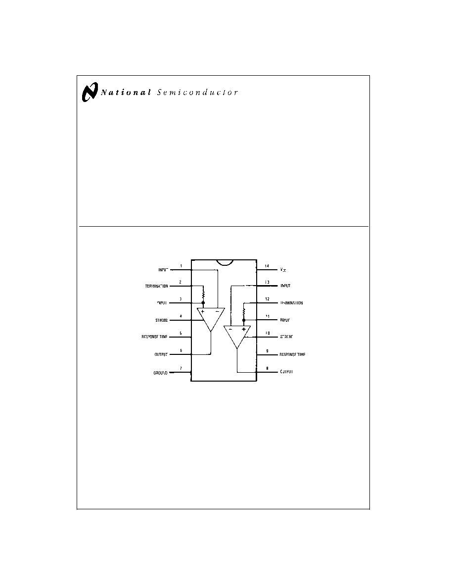
Connection Diagram
Dual-In-Line Package
DS005796-2
Top View
For Complete Military 883 Specifications, See RETS Data Sheet.
Order Number: DS7820J/883
See NS Package Number J14A
September 1999
DS7820
Dual
Line
Receiver
© 1999 National Semiconductor Corporation
DS005796
www.national.com
Absolute Maximum Ratings
(Note 2)
If Military/Aerospace specified devices are required,
please contact the National Semiconductor Sales Office/
Distributors for availability and specifications.
Supply Voltage
8.0V
Input Voltage
Ī
20V
Differential Input Voltage
Ī
20V
Strobe Voltage
8.0V
Output Sink Current
25 mA
Storage Temperature Range
-65įC to +150įC
Lead Temperature (Soldering, 4 sec.)
260įC
Maximum Power Dissipation at 25įC
(Note 1)
1308 mW
Operating Conditions
Min
Max
Units
Supply Voltage (V
CC
)
4.5
5.5
V
Temperature (T
A
)
-55
+125
įC
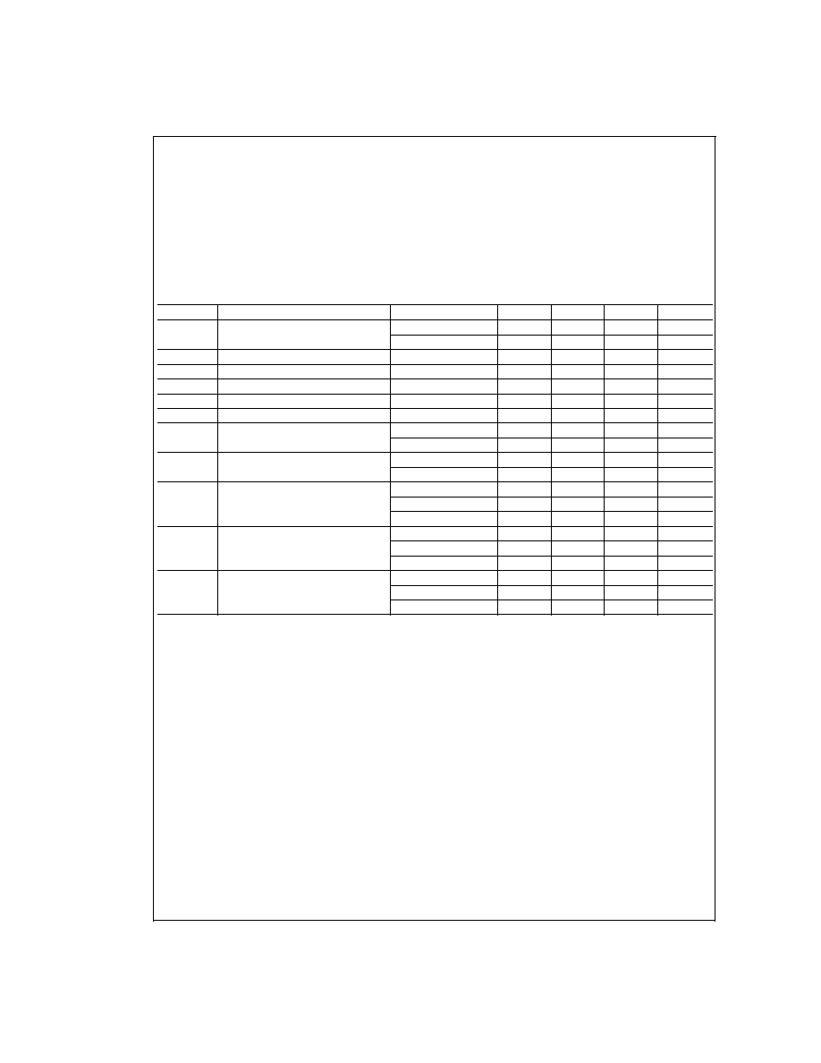
Electrical Characteristics
(Notes 3, 4)
Symbol
Parameter
Conditions
Min
Typ
Max
Units
V
TH
Input Threshold Voltage
V
CM
= 0V
-0.5
0
0.5
V
-15V
V
CM
15V
-1.0
0
1.0
V
V
OH
High Output Level
I
OUT
0.2 mA
2.5
5.5
V
V
OL
Low Output Level
I
SINK
3.5 mA
0
0.4
V
R
I
-
Inverting Input Resistance
3.6
5.0
k
R
I
+
Non-Inverting Input Resistance
1.8
2.5
k
R
T
Line Termination Resistance
T
A
= 25įC
120
170
250
t
r
Response Time
C
DELAY
= 0 pF
40
ns
C
DELAY
= 100 pF
150
ns
I
ST
Strobe Current
V
STROBE
= 0.4V
-1.0
-1.4
mA
V
STROBE
= 5.5V
5.0
ĶA
I
CC
Power Supply Current
V
IN
= 15V
3.2
6.0
mA
V
IN
= 0V
5.8
10.2
mA
V
IN
= -15V
8.3
15.0
mA
I
IN
+
Non-Inverting Input Current
V
IN
= 15V
5.0
7.0
mA
V
IN
= 0V
-1.6
-1.0
mA
V
IN
= -15V
-9.8
-7.0
mA
I
IN
-
Inverting Input Current
V
IN
= 15V
3.0
4.2
mA
V
IN
= 0V
0
-0.5
mA
V
IN
= -15V
-4.2
-3.0
mA
Note 1: Derate cavity package 8.7 mW/įC above 25įC.
Note 2: "Absolute Maximum Ratings" are those values beyond which the safety of the device cannot be guaranteed. Except for "Operating Temperature Range" they
are not meant to imply that the devices should be operated at these limits. The table of "Electrical Characteristics" provides conditions for actual device operation.
Note 3: These specifications apply for 4.5V
V
CC
5.5V, -15V
V
CM
15V and -55įC
T
A
+125įC unless otherwise specified; typical values given are for V
CC
= 5.0V, T
A
= 25įC and V
CM
= 0 unless stated differently.
Note 4: All currents into device pins shown as positive, out of device pins as negative, all voltages referenced to ground unless otherwise noted. All values shown
as max or min on absolute value basis.
Note 5: The specifications and curves given are for one side only. Therefore, the total package dissipation and supply currents will be double the values given when
both receivers are operated under identical conditions.
www.national.com
2

Typical Performance Characteristics
(Note 4)
Supply Voltage Sensitivity
DS005796-16
Common Mode Rejection
DS005796-17
Transfer Function
DS005796-18
Response Time
DS005796-19
Output Voltage Levels
DS005796-20
Termination Resistance
DS005796-21
Positive Supply Current
DS005796-22
Internal Power Dissipation
DS005796-23
www.national.com
3
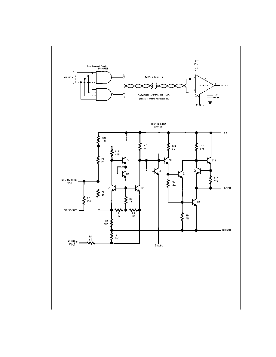
Typical Application
Schematic Diagram
DS005796-3
DS005796-1
www.national.com
4
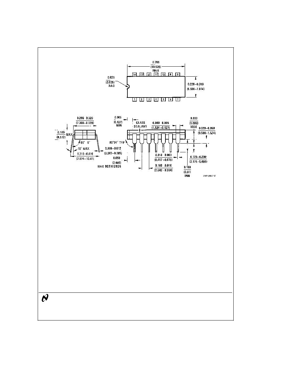
Physical Dimensions
inches (millimeters) unless otherwise noted
LIFE SUPPORT POLICY
NATIONAL'S PRODUCTS ARE NOT AUTHORIZED FOR USE AS CRITICAL COMPONENTS IN LIFE SUPPORT
DEVICES OR SYSTEMS WITHOUT THE EXPRESS WRITTEN APPROVAL OF THE PRESIDENT AND GENERAL
COUNSEL OF NATIONAL SEMICONDUCTOR CORPORATION. As used herein:
1. Life support devices or systems are devices or
systems which, (a) are intended for surgical implant
into the body, or (b) support or sustain life, and
whose failure to perform when properly used in
accordance with instructions for use provided in the
labeling, can be reasonably expected to result in a
significant injury to the user.
2. A critical component is any component of a life
support device or system whose failure to perform
can be reasonably expected to cause the failure of
the life support device or system, or to affect its
safety or effectiveness.
National Semiconductor
Corporation
Americas
Tel: 1-800-272-9959
Fax: 1-800-737-7018
Email: support@nsc.com
National Semiconductor
Europe
Fax: +49 (0) 1 80-530 85 86
Email: europe.support@nsc.com
Deutsch Tel: +49 (0) 1 80-530 85 85
English
Tel: +49 (0) 1 80-532 78 32
FranÁais Tel: +49 (0) 1 80-532 93 58
Italiano
Tel: +49 (0) 1 80-534 16 80
National Semiconductor
Asia Pacific Customer
Response Group
Tel: 65-2544466
Fax: 65-2504466
Email: sea.support@nsc.com
National Semiconductor
Japan Ltd.
Tel: 81-3-5639-7560
Fax: 81-3-5639-7507
www.national.com
Ceramic Dual-In-Line Package (J)
Order Number DS7820J/883
NS Package Number J14A
DS7820
Dual
Line
Receiver
National does not assume any responsibility for use of any circuitry described, no circuit patent licenses are implied and National reserves the right at any time without notice to change said circuitry and specifications.