DS7830
Dual Differential Line Driver
General Description
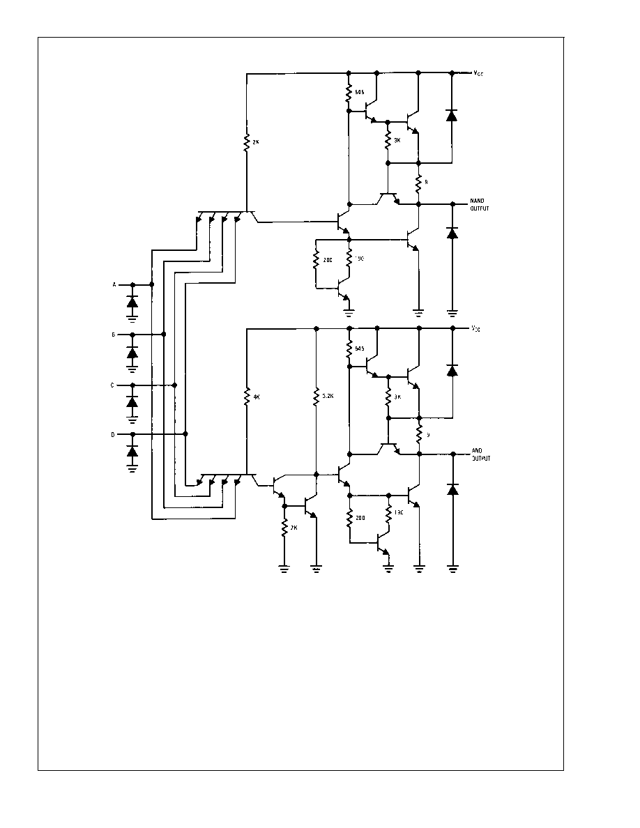
The DS7830 is a dual differential line driver that also per-
forms the dual four-input NAND or dual four-input AND func-
tion.
TTL (Transistor-Transistor-Logic) multiple emitter inputs al-
low this line driver to interface with standard TTL systems.
The differential outputs are balanced and are designed to
drive long lengths of coaxial cable, strip line, or twisted pair
transmission lines with characteristic impedances of 50
to
500
. The differential feature of the output eliminates
troublesome ground-loop errors normally associated with
single-wire transmissions.
Features
n
Single 5V power supply
n
Diode protected outputs for termination of positive and
negative voltage transients
n
Diode protected inputs to prevent line ringing
n
High speed
n
Short circuit protection
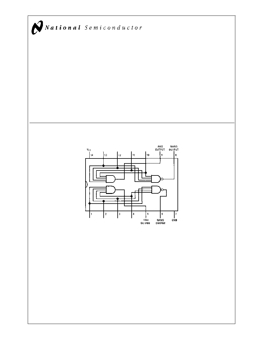
Connection Diagram
Dual-In-Line and Flat Package
DS005799-2
Top View
For Complete Military 883 Specificatons, See RETS Data Sheet.
Order Number DS7830J/883 or DS7830W/883
See NS Package Number J14A
August 2000
DS7830
Dual
Differential
Line
Driver
� 2000 National Semiconductor Corporation
DS005799
www.national.com

Absolute Maximum Ratings
(Note 2)
If Military/Aerospace specified devices are required,
please contact the National Semiconductor Sales Office/
Distributors for availability and specifications.
V
CC
7.0V
Input Voltage
5.5V
Storage Temperature
-65�C to +150�C
Lead Temperature (Soldering, 4 sec.)
260�C
Output Short Circuit Duration (125�C)
1 second
Maximum Power Dissipation (Note 1)
at 25�C
Cavity Package
1308 mW
Operating Conditions
Min
Max
Units
Supply Voltage (V
CC
)
DS7830
4.5
5.5
V
Temperature (T
A
)
DS7830
-55
+125
�C
Note 1: Derate cavity package 8.7 mW/�C above 25�C; derate molded pack-
age 9.7 mW/�C above 25�C.
Electrical Characteristics
(Notes 3, 4)
Symbol
Parameter
Conditions
Min
Typ
Max
Units
V
IH
Logical "1" Input Voltage
2.0
V
V
IL
Logical "0" Input Voltage
0.8
V
V
OH
Logical "1" Output Voltage
V
IN
= 0.8V
I
OUT
= -0.8 mA
2.4
V
I
OUT
= 40 mA
1.8
3.3
V
V
OL
Logical "0" Output Voltage
V
IN
= 2.0V
I
OUT
= 32 mA
0.2
0.4
V
I
OUT
= 40 mA
0.22
0.5
V
I
IH
Logical "1" Input Current
V
IN
= 2.4V
120
�A
V
IN
= 5.5V
2
mA
I
IL
Logical "0" Input Current
V
IN
= 0.4V
-4.8
mA
I
SC
Output Short Circuit Current
V
CC
= 5.0V, T
A
= 125�C, (Note 5)
-40
-100
-120
mA
I
CC
Supply Current
V
IN
= 5.0V, (Each Driver)
11
18
mA
V
I
Input Clamp
V
CC
= Min, I
IN
= - 12 mA
-1.0
-1.5
V
Switching Characteristics
T
A
= 25�C, V
CC
= 5V, unless otherwise noted
Symbol
Parameter
Conditions
Min
Typ
Max
Units
t
pd1
Propagation Delay AND Gate
R
L
= 400
, C
L
= 15 pF
8
12
ns
t
pd0
(
Figure 1 )
11
18
ns
t
pd1
Propagation Delay NAND Gate
R
L
= 400
, C
L
= 15 pF
8
12
ns
t
pd0
(
Figure 1 )
5
8
ns
t
1
Differential Delay
Load, 100
and 5000 pF,
12
16
ns
(
Figure 2 )
t
2
Differential Delay
Load, 100
and 5000 pF,
12
16
ns
(
Figure 2 )
Note 2: "Absolute Maximum Ratings" are those values beyond which the safety of the device cannot be guaranteed. Except for "Operating Temperature Range" they
are not meant to imply that the devices should be operated at these limits. The table of "Electrical Characteristics" provides conditions for actual device operation.
Note 3: Unless otherwise specified min/max limits apply across the -55�C to +125�C temperature range for the DS7830. Typical values are for T
A
= 25�C and V
CC
= 5.0V.
Note 4: All currents into device pins shown as positive, out of device pins as negative, all voltages referenced to ground unless otherwise noted. All values shown
as max or min on absolute value basis.
Note 5: Only one output at a time should be shorted.
DS7830
www.national.com
2
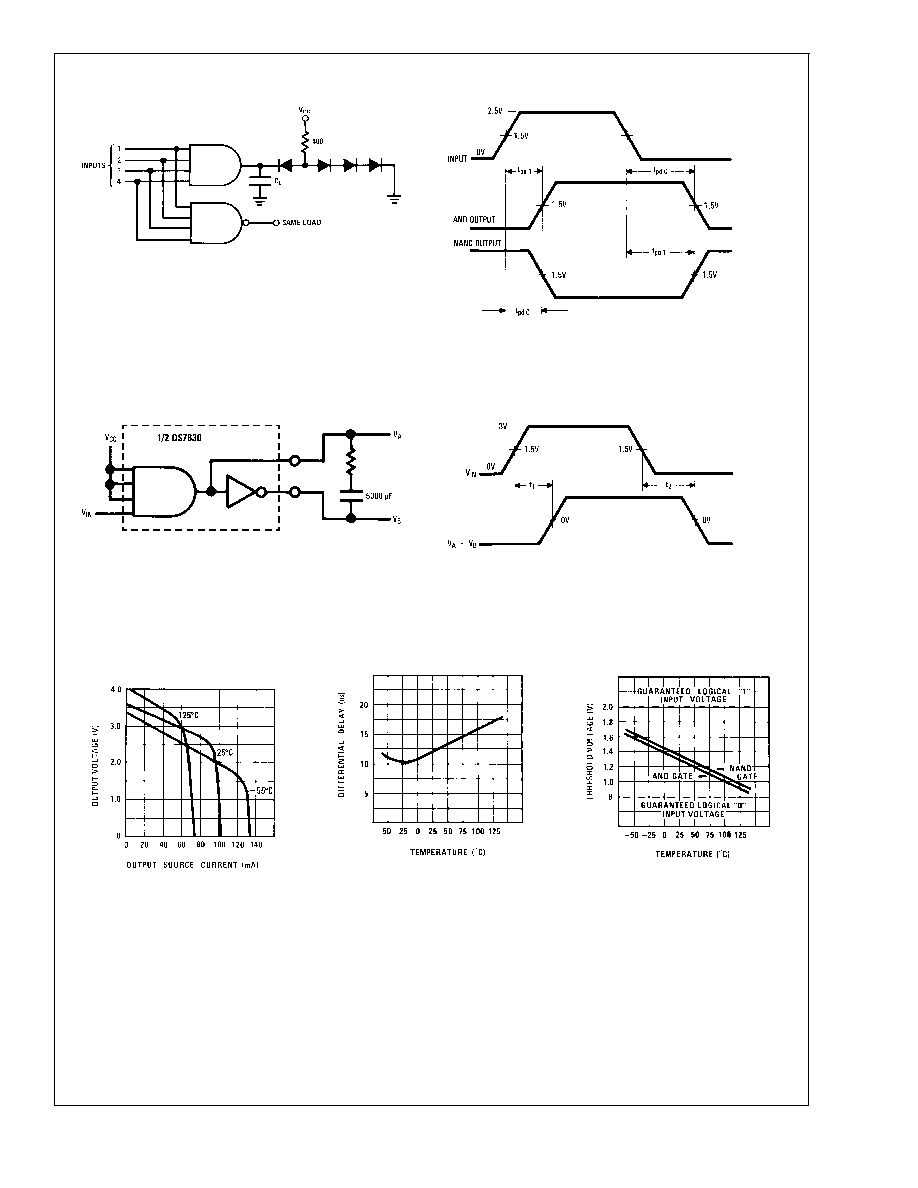
AC Test Circuit and Switching Time Waveforms
Typical Performance Characteristics
DS005799-4
DS005799-9
f = 1 MHz
t
r
= t
f
10 ns (10% to 90%)
Duty cycle = 50%
FIGURE 1.
DS005799-8
DS005799-10
FIGURE 2.
Output High Voltage
(Logical "1")
vs Ouput Current
DS005799-7
Differential Delay vs
Temperature
DS005799-11
Threshold Voltage
vs Temperature
DS005799-12
DS7830
www.national.com
3

Typical Performance Characteristics
(Continued)
Typical Application
Differential Output Voltage
(|V
AND
- V
NAND
| ) vs
Differential Output Current
DS005799-13
Power Dissipation (No Load)
vs Data Input Frequency
DS005799-14
Output Low Voltage
(Logical "0") vs
Output Current
DS005799-15
Digital Data Transmission
DS005799-3
Exact value depends on line length.
*Optional to control response time.
DS7830
www.national.com
4