
TL F 5810
DS7836DS8836
Quad
NOR
Unified
Bus
Receiver
February 1996
DS7836 DS8836 Quad NOR Unified Bus Receiver
General Description
The DS7836 DS8836 are quad 2-input receivers designed
for use in bus organized data transmission systems inter-
connected by terminated 120X impedance lines The exter-
nal termination is intended to be 180X resistor from the bus
to the
a
5V logic supply together with a 390X resistor from
the bus to ground The design employs a built-in input hys-
teresis providing substantial noise immunity Low input cur-
rent allows up to 27 driver receiver pairs to utilize a com-
mon bus Performance is optimized for systems with bus
rise and fall times
s
1 0 ms V
Features
Y
Low input current with normal V
CC
or V
CC
e
0V
(15 mA typ)
Y
Built-in input hysteresis (1V typ)
Y
High noise immunity (2V typ)
Y
Temperature-insensitive input thresholds track bus logic
levels
Y
TTL compatible output
Y
Matched optimized noise immunity for ``1'' and ``0''
levels
Y
High speed (18 ns typ)
Typical Application
120X Unified Data Bus
TL F 5810 � 1
Connection Diagram
Dual-In-Line Package
TL F 5810 � 2
Top View
Order Number DS7836J or DS8836N
See NS Package Number J14A or N14A
C1996 National Semiconductor Corporation
RRD-B30M36 Printed in U S A
http
www national com

Absolute Maximum Ratings
If Military Aerospace specified devices are required
please contact the National Semiconductor Sales
Office Distributors for availability and specifications
Supply Voltage
7 0V
Current Voltage
5 5V
Storage Temperature Range
b
65 C to
a
150 C
Maximum Power Dissipation at 25 C
Cavity Package
1308 mW
Molded Package
1207 mW
Lead Temperature (Soldering 4 seconds)
260 C
Derate cavity package 8 7 mW C above 25 C derate molded package 9 7
mW C above 25 C
Operating Conditions
Min
Max
Units
Supply Voltage (V
CC
)
DS7836
4 5
5 5
V
DS8836
4 75
5 25
V
Temperature (T
A
)
DS7836
b
55
a
125
C
DS8836
0
a
70
C
Electrical Characteristics
The following apply for V
MIN
s
V
CC
s
V
MAX
T
MIN
s
T
A
s
T
MAX
unless otherwise specified (Notes 2 and 3)
Symbol
Parameter
Conditions
Min
Typ
Max
Units
V
TH
High Level Input Threshold
V
CC
e
Max
DS7836
1 65
2 25
2 65
V
DS8836
1 80
2 25
2 50
V
V
IL
Low Level Input Threshold
V
CC
e
Min
DS7836
0 97
1 30
1 63
V
DS8836
1 05
1 30
1 55
V
I
IN
Maximum Input Current
V
IN
e
4V
V
CC
e
Max
15
50
m
A
V
CC
e
0V
1
50
m
A
V
OH
Logical ``1'' Output Voltage
V
IN
e
0 5V I
OUT
e b
400 mA
2 4
V
V
OL
Logical ``0'' Output Voltage
V
IN
e
4V I
OUT
e
16 mA
0 25
0 4
V
I
SC
Output Short Circuit Current
V
IN
e
0 5V V
OUT
e
0V V
CC
e
Max (Note 4)
b
18
b
55
mA
I
CC
Power Supply Current
V
IN
e
4V (Per Package)
25
40
mA
V
CL
Input Clamp Diode Voltage
I
IN
e b
12 mA T
A
e
25 C
b
1
b
1 5
V
Switching Characteristics
V
CC
e
5V T
A
e
25 C unless otherwise specified
Symbol
Parameter
Conditions
Min
Typ
Max
Units
t
pd
Propagation Delays
(Notes 4 and 5)
Input to Logical ``1'' Output
20
30
ns
Input to Logical ``0'' Output
18
30
ns
Note 1
``Absolute Maximum Ratings'' are those values beyond which the safety of the device cannot be guaranteed Except for ``Operating Temperature Range''
they are not meant to imply that the devices should be operated at these limits The table of ``Electrical Characteristics'' provides conditions for actual device
operation
Note 2
Unless otherwise specified min max limits apply across the
b
55 C to
a
125 C temperature range for the DS7836 and across the 0 C to
a
70 C range for
the DS8836 All typical values are for T
A
e
25 C and V
CC
e
5V
Note 3
All currents into device pins shown as positive out of device pins as negative all voltages referenced to ground unless otherwise noted All values shown
as max or min on absolute value basis
Note 4
Fan-out of 10 load C
LOAD
e
15 pF total measured from V
IN
e
1 3V to V
OUT
e
1 5V V
IN
e
0V to 3V pulse
Note 5
Fan-out of 10 load C
LOAD
e
15 pF total measured from V
IN
e
2 3V to V
OUT
e
1 5V V
IN
e
0V to 3V pulse
http
www national com
2
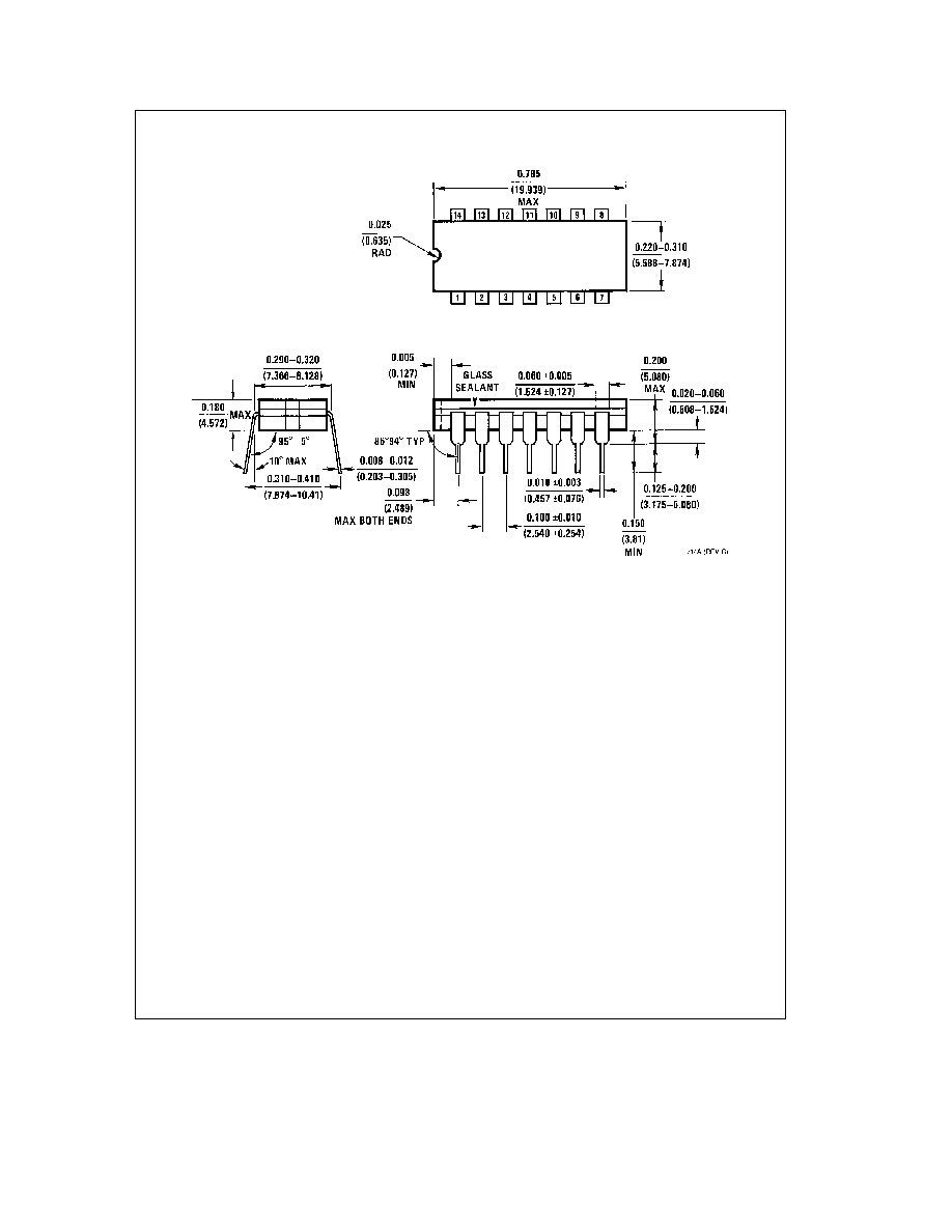
Physical Dimensions
inches (millimeters)
Ceramic Dual-In-Line Package (J)
Order Number DS7836J
NS Package Number J14A
http
www national com
3
DS7836DS8836
Quad
NOR
Unified
Bus
Receiver
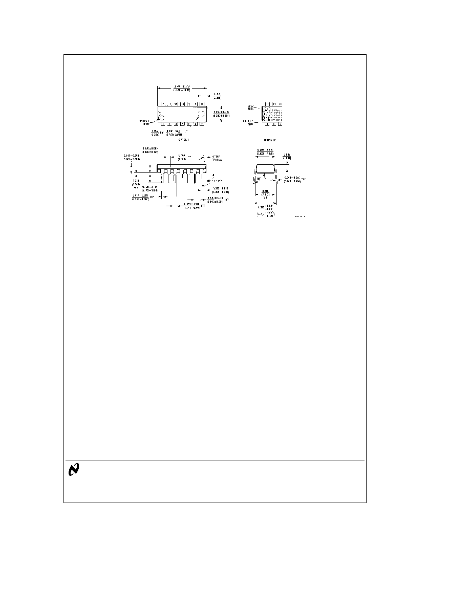
Physical Dimensions
inches (millimeters) (Continued)
Molded Dual-In-Line Package (N)
Order Number DS8836N
NS Package Number N14A
LIFE SUPPORT POLICY
NATIONAL'S PRODUCTS ARE NOT AUTHORIZED FOR USE AS CRITICAL COMPONENTS IN LIFE SUPPORT
DEVICES OR SYSTEMS WITHOUT THE EXPRESS WRITTEN APPROVAL OF THE PRESIDENT OF NATIONAL
SEMICONDUCTOR CORPORATION As used herein
1 Life support devices or systems are devices or
2 A critical component is any component of a life
systems which (a) are intended for surgical implant
support device or system whose failure to perform can
into the body or (b) support or sustain life and whose
be reasonably expected to cause the failure of the life
failure to perform when properly used in accordance
support device or system or to affect its safety or
with instructions for use provided in the labeling can
effectiveness
be reasonably expected to result in a significant injury
to the user
National Semiconductor
National Semiconductor
National Semiconductor
National Semiconductor
Corporation
Europe
Hong Kong Ltd
Japan Ltd
1111 West Bardin Road
Fax a49 (0) 180-530 85 86
13th Floor Straight Block
Tel 81-043-299-2308
Arlington TX 76017
Email europe support nsc com
Ocean Centre 5 Canton Rd
Fax 81-043-299-2408
Tel 1(800) 272-9959
Deutsch Tel a49 (0) 180-530 85 85
Tsimshatsui Kowloon
Fax 1(800) 737-7018
English
Tel a49 (0) 180-532 78 32
Hong Kong
Fran ais Tel a49 (0) 180-532 93 58
Tel (852) 2737-1600
http
www national com
Italiano
Tel a49 (0) 180-534 16 80
Fax (852) 2736-9960
National does not assume any responsibility for use of any circuitry described no circuit patent licenses are implied and National reserves the right at any time without notice to change said circuitry and specifications