DS3650
Quad Differential Line Receivers
General Description
The DS3650 is TTL compatible quad high speed circuits in-
tended primarily for line receiver applications. Switching
speeds have been enhanced over conventional line receiv-
ers by the use of Schottky technology, and TRI-STATE
Æ
strobing is incorporated offering a high impedance output
state for bussed organizations.
The DS3650 has active pull-up outputs and offers a
TRI-STATE strobe.
Features
n
High speed
n
TTL compatible
n
Input sensitivity:
±
25 mV
n
TRI-STATE outputs for high speed busses
n
Standard supply voltages:
±
5V
n
Pin and function compatible with MC3450
Connection Diagram
Input
Strobe
Output
DS3650
V
D
25 mV
L
H
H
Open
-25 mV
V
ID
25 mV
L
X
H
Open
V
ID
-25 mV
L
L
H
Open
L = Low Logic State
Open = TRI-STATE
H = High Logic State X = Indeterminate State
TRI-STATE
Æ
is a registered trademark of National Semiconductor Corporation.
Dual-In-Line Package
DS005782-1
Top View
Order Number DS3650M or DS3650N
See NS Package Number M16A or N16A
For Complete Military 883 Specifications,
see RETS Data Sheet.
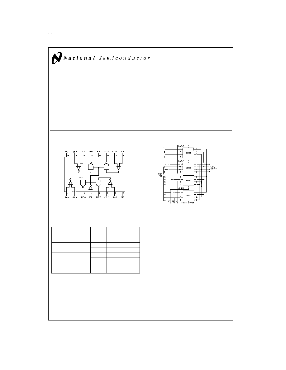
Wired "OR" Data Selecting Using TRI-STATE Logic
DS005782-3
June 1999
DS3650
Quad
Differential
Line
Receivers
© 1999 National Semiconductor Corporation
DS005782
www.national.com
Absolute Maximum Ratings
(Note 2)
If Military/Aerospace specified devices are required,
please contact the National Semiconductor Sales Office/
Distributors for availability and specifications.
Power Supply Voltages
V
CC
+7.0 V
DC
V
EE
-7.0 V
DC
Differential-Mode Input Signal Voltage
Range, V
IDR
±
6.0 V
DC
Common-Mode Input Voltage Range,
V
ICR
±
5.0 V
DC
Strobe Input Voltage, V
I(S)
5.5 V
DC
Storage Temperature Range
-65∞C to +150∞C
Lead Temperature
(Soldering, 4 seconds)
260∞C
Maximum Power Dissipation (Note 1)
at 25∞C
Cavity Package
1509 mW
Molded DIP Package
1476 mW
SO Package
1051 mW
Operating Conditions
Min
Max
Units
Supply Voltage, V
CC
4.75
5.25
V
DC
Supply Voltage, V
EE
-4.75
-5.25
V
DC
Operating Temperature, T
A
0
+70
∞C
Output Load Current, I
OL
16
mA
Differential-Mode Input
Voltage Range, V
IDR
-5.0
+5.0
V
DC
Common-Mode Input
Voltage Range, V
ICR
-3.0
+3.0
V
DC
Input Voltage Range
Input to GND, V
IR
-5.0
+3.0
V
DC
Note 1: Derate cavity package 10.1 mW/∞C above 25∞C; derate molded DIP
package 11.8 mW/∞C above 25∞C; derate SO package 8.41 mW/∞C above
25∞C.
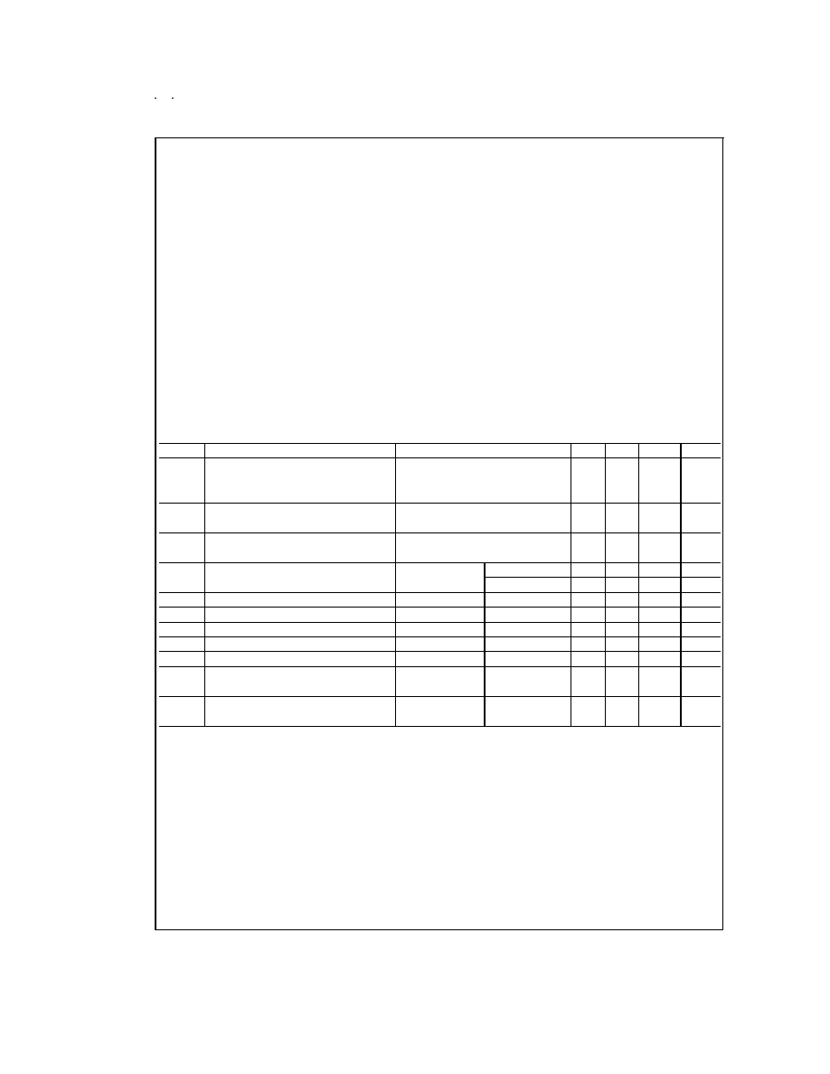
Electrical Characteristics
(Notes 3, 4)
(V
CC
= 5.0 V
DC
, V
EE
= -5.0 V
DC
, Min
T
A
Max, unless otherwise noted)
Symbol
Parameter
Conditions
Min
Typ
Max
Units
V
IS
Input Sensitivity, (Note 6)
(Common-Mode Voltage Range =
Min
V
CC
Max
±
25.0
mV
-3V
V
IN
3V)
Min
V
EE
Max
I
IH(I)
High Level Input Current to
(
Figure 5 )
75
µA
Receiver Input
I
IL(I)
Low Level Input Current to
(
Figure 6 )
-10
µA
Receiver Input
I
IH(S)
High Level Input Current to Strobe Input
(
Figure 3 )
V
IH(S)
= 2.4V
40
µA
V
IH(S)
= V
CC
1
mA
I
IL(S)
Low Level Input Current to Strobe Input
V
IH(S)
= 0.4V
-1.6
mA
V
OH
High Level Output Voltage
(
Figure 1 )
2.4
V
V
OL
Low Level Output Voltage
(
Figure 1 )
0.45
V
I
OS
Short-Circuit Output Current (Note 5)
(
Figure 4 )
-18
-70
mA
I
OFF
Output Disable Leakage Current
(
Figure 7 )
40
µA
I
CCH
High Logic Level Supply Current
(
Figure 2 )
45
60
mA
from V
CC
I
EEH
High Logic Level Supply Current
(
Figure 2 )
-17
-30
mA
from V
EE
Note 2: "Absolute Maximum Ratings" are those values beyond which the safety of the device cannot be guaranteed. Except for "Operating Temperature Range" they
are not meant to imply that the devices should be operated at these limits. The table of "Electrical Characteristics" provides conditions for actual device operation.
Note 3: Unless otherwise specified, min/max limits apply across the 0∞C to +70∞C range for the DS3650. All typical values are for T
A
= 25∞C, V
CC
= 5V and V
EE
=
-5V.
Note 4: All currents into device pins shown as positive, out of device pins as negative, all voltages referenced to ground unless otherwise noted. All values shown
as max or min on absolute value basis.
Note 5: Only one output at a time should be shorted.
Note 6: A parameter which is of primary concern when designing with line receivers is, what is the minimum differential input voltage required as the receiver input
terminals to guarantee a given output logic state. This parameter is commonly referred to as threshold voltage. It is well known that design considerations of threshold
voltage are plagued by input offset currents, bias currents, network source resistances, and voltage gain. As a design convenience, the DS3650 is specified to a pa-
rameter called input sensitivity (V
IS
). This parameter takes into consideration input offset currents and bias currents and guarantees a minimum input differential volt-
age to cause a given output logic state with respect to a maximum source impedance of 200
at each input.
www.national.com
2
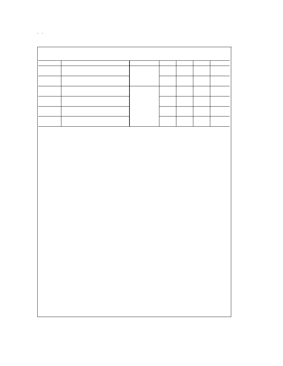
Switching Characteristics
(V
CC
= 5 V
DC
, V
EE
= -5 V
DC
, T
A
= 25∞C unless otherwise noted)
Symbol
Parameter
Conditions
Min
Typ
Max
Units
t
PHL(D)
High-to-Low Logic Level Propagation
21
25
ns
Delay Time (Differential Inputs)
(
Figure 8 )
t
PLH(D)
Low-to-High Logic Level Propagation
20
25
ns
Delay Time (Differential Inputs)
t
POH(S)
TRI-STATE to High Logic Level
16
21
ns
Propagation Delay Time (Strobe)
t
PHO(S)
High Logic Level to TRI-STATE
7
18
ns
Propagation Delay Time (Strobe)
(
Figure 9 )
t
POL(S)
TRI-STATE to Low Logic Level
19
27
ns
Propagation Delay Time (Strobe)
t
PLO(S)
Low Logic Level to TRI-STATE
14
29
ns
Propagation Delay Time (Strobe)
www.national.com
3

(Continued)
DS005782-7
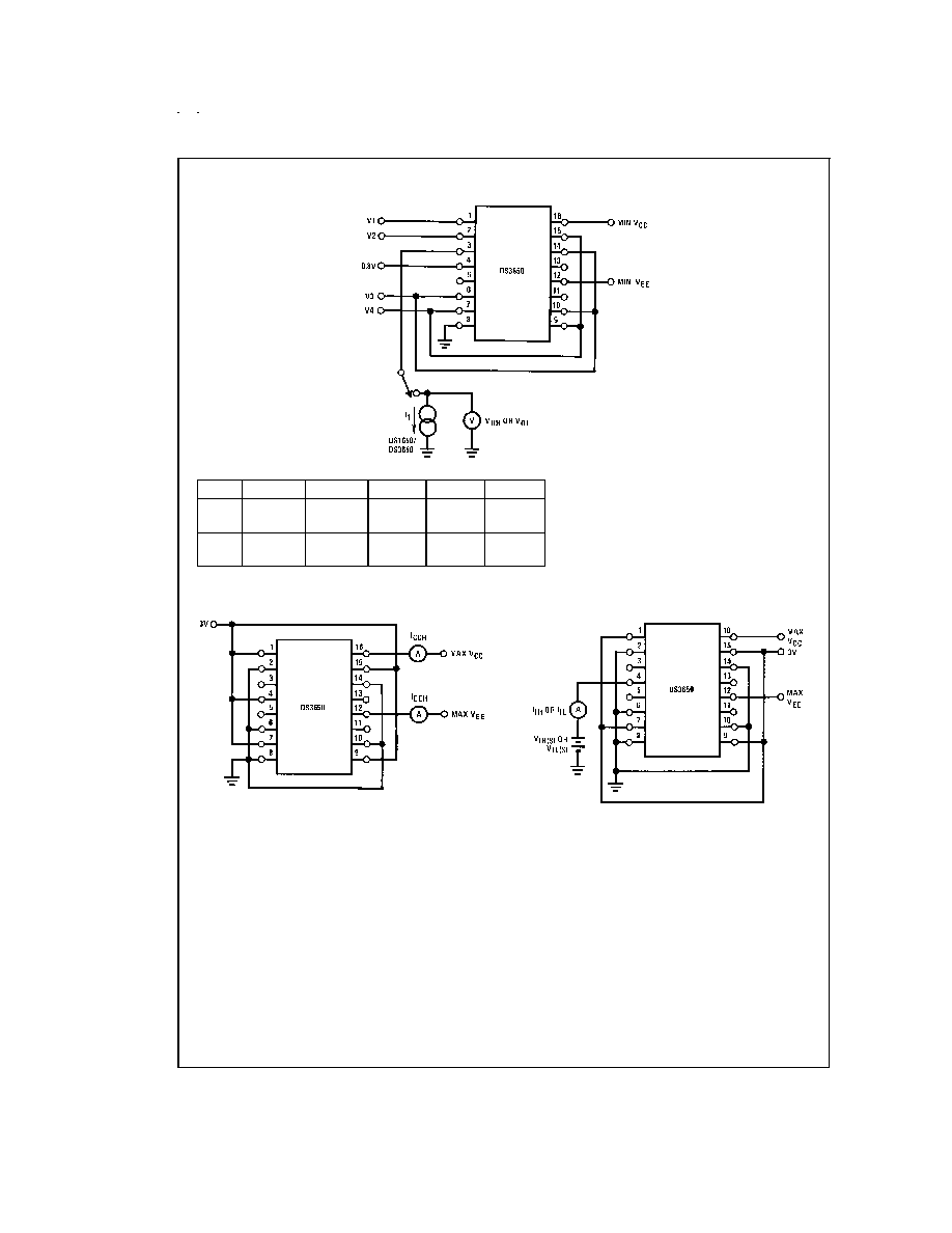
Note: Channel A shown under test, other channels are tested similiarly.
Only one output shorted at a time.
FIGURE 4. I
OS
DS005782-8
Note: Channel A(-) shown under test, other channels are tested similarly.
Devices are tested with V1 from 3V to -3V.
FIGURE 5. I
IH
DS005782-9
Note: Channel A(-) shown under test, other channels are tested similarly.
Devices are tested with V1 from 3V to -3V.
FIGURE 6. I
IL
DS005782-10
Note: Output of Channel A shown under test, other outputs are
testedsimilarly for V1 = 0.4V and 2.4V.
FIGURE 7. I
OFF
www.national.com
5