DS78LS120
Dual Differential Line Receiver (Noise Filtering and
Fail-Safe)
General Description
The DS78LS120 is a high performance, dual differential, TTL
compatible line receiver for both balanced and unbalanced
digital data transmission. The inputs are compatible with
EIA, Federal and MIL standards.
The line receiver will discriminate a
±
200 mV input signal
over a common-mode range of
±
10V and a
±
300 mV signal
over a range of
±
15V.
Circuit features include hysteresis and response control for
applications where controlled rise and fall times and/or high
frequency noise rejection are desirable. Threshold offset
control is provided for fail-safe detection, should the input be
open or short. Each receiver includes an optional 180
ter-
minating resistor and the output gate contains a logic strobe
for time discrimination. The DS78LS120 is specified over a
-55∞C to +125∞C temperature range.
Input specifications meet or exceed those of the popular
DS7820 line receiver.
Features
n
Meets EIA standards RS232-C, RS422 and RS423,
Federal Standards 1020, 1030 and MIL-188-114
n
Input voltage range of
±
15V (differential or
common-mode)
n
Separate strobe input for each receiver
n
5k typical input impedance
n
Optional 180
termination resistor
n
50mV input hysteresis
n
200mV input threshold
n
Separate fail-safe mode
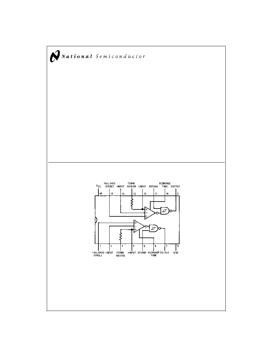
Connection Diagram
Dual-In-Line-Package
DS007499-1
Top View
see RETS Data Sheet.
Order Number DS78LS120J/883 or DS78LS120W/883
See NS Package Number J16A or W16A
September 1999
DS78LS120
Dual
Differential
Line
Receiver
(Noise
Filtering
and
Fail-Safe)
© 1999 National Semiconductor Corporation
DS007499
www.national.com

Absolute Maximum Ratings
(Note 2)
If Military/Aerospace specified devices are required,
please contact the National Semiconductor Sales Office/
Distributors for availability and specifications.
Supply Voltage
7V
Input Voltage
±
25V
Strobe Voltage
7V
Output Sink Current
50 mA
Storage Temperature Range
-65∞C to +150∞C
Maximum Power Dissipation at 25∞C
(Note 1)
1433 mV
Lead Temperature (Soldering, 4 sec)
260∞C
Operating Conditions
Min
Max
Units
Supply Voltage (V
CC
)
4.5
5.5
V
Temperature (T
A
)
-55
+125
∞C
Common-Mode Voltage (V
CM
)
-15
+15
V
Electrical Characteristics
(Notes 3, 4)
Symbol
Parameter
Conditions
Min
Typ
Max
Units
V
TH
Differential Threshold Voltage
I
OUT
= -400 µA, V
OUT
2.5V
-7V
V
CM
7V
0.06
0.2
V
-15
V
CM
15V
0.06
0.3
V
V
TL
Differential Threshold Voltage
I
OUT
= 4 mA, V
OUT
0.5V
-7V
V
CM
7V
-0.08
-0.2
V
-15V
V
CM
15V
-0.08
-0.3
V
V
TH
Differential Threshold Voltage
I
OUT
= -400 µA, V
OUT
2.5V
-7V
V
CM
7V
0.47
0.7
V
V
TL
with Fail-Safe Offset = 5V
I
OUT
= 4 mA, V
OUT
0.5V
-7V
V
CM
7V
-0.2 -0.42
V
R
IN
Input Resistance
-15V
V
CM
15V, 0V
V
CC
7V
4
5
k
R
T
Line Termination Resistance
T
A
= 25∞C
100
180
300
R
O
Offset Control Resistance
T
A
= 25∞C
42
56
70
k
I
IND
Data Input Current (Unterminated)
V
CM
= 10V
2
3.1
mA
V
CM
= 0V
0V
V
CC
7V
0
-0.5
mA
V
CM
= -10V
-2
-3.1
mA
V
THB
Input Balance
I
OUT
= -400 µA, V
OUT
2.5V,
-7V
V
CM
7V
0.1
0.4
V
(Note 6)
R
S
= 500
I
OUT
= 4 mA, V
OUT
0.5V,
-7V
V
CM
7V
-0.1
-0.4
V
R
S
= 500
V
OH
Logical "1" Output Voltage
I
OUT
= -400 µA, V
DIFF
= 1V, V
CC
= 4.5V
2.5
3
V
V
OL
Logical "0" Output Voltage
I
OUT
= 4 mA, V
DIFF
= -1V, V
CC
= 4.5V
0.35
0.5
V
I
CC
Power Supply Current
V
CC
= 5.5V
V
CM
= 15V
10
16
mA
V
DIFF
= -0.5V, (Both Receivers)
V
CM
= -15V
10
16
mA
I
IN (1)
Logical "1" Strobe Input Current
V
STROBE
= 5.5V, V
DIFF
= 3V
1
100
µA
I
IN (0)
Logical "0" Strobe Input Current
V
STROBE
= 0V, V
DIFF
= -3V
-290 -400
µA
V
IH
Logical "1" Strobe Input Voltage
V
OL
0.5, I
OUT
= 4mA
2.0
1.12
V
V
IL
Logical "0" Strobe Input Voltage
V
OH
2.5V, I
OUT
, = -400 µA
1.12
0.8
V
I
OS
Output Short-Circuit Current
V
OUT
= 0V, V
CC
= 5.5V, V
STROBE
= 0V,(Note 5)
-30
-100 -170
mA
Note 1: Derate cavity package 9.6 mW/∞C above 25∞C.
Note 2: "Absolute Maximum Ratings" are those values beyond which the safety of the device cannot be guaranteed. Except for "Operating Temperature Range" they
are not meant to imply that the devices should be operated at these limits. The table of "Electrical Characteristics" provides conditions for actual device operation.
Note 3: Unless otherwise specified min/max limits apply across the -55∞C to +125∞C temperature range for the DS78LS120. All typical values are for T
A
= 25∞C, V
CC
= 5V and V
CM
= 0V.
Note 4: All currents into device pins shown as positive, out of device pins as negative, all voltages referenced to ground unless otherwise noted. All values shown
as max or min on absolute value basis.
Note 5: Only one output at a time should be shorted.
Note 6: Refer to EIA-RS422 for exact conditions.
Switching Characteristics
V
CC
= 5V, T
A
= 25∞C
Symbol
Parameter
Conditions
Min
Typ
Max
Units
t
pd0(D)
Differential Input to "0" Output
38
60
ns
t
pd1(D)
Differential Input to "1" Output
Response Pin Open, C
L
= 15 pF, R
L
= 2 k
38
60
ns
www.national.com
2
Switching Characteristics
(Continued)
V
CC
= 5V, T
A
= 25∞C
Symbol
Parameter
Conditions
Min
Typ
Max
Units
t
pd0(S)
Strobe Input to "0" Output
16
25
ns
t
pd1(S)
Strobe Input to "1" Output
12
25
ns
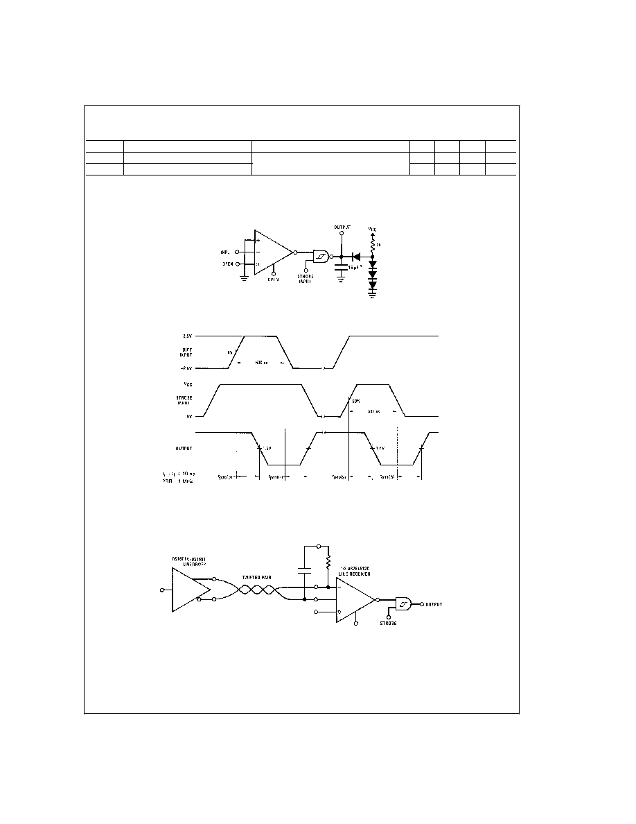
AC Test Circuit and Switching Time Waveforms
Application Hints
Differential and Strobe Input Signal
DS007499-3
Includes probe and test fixture capacitance
DS007499-4
Note: Optimum switching response is obtained by minimizing stray capacitance on Response Control pin (no external connection).
Balanced Data Transmission
DS007499-5
www.national.com
3
Application Hints
(Continued)
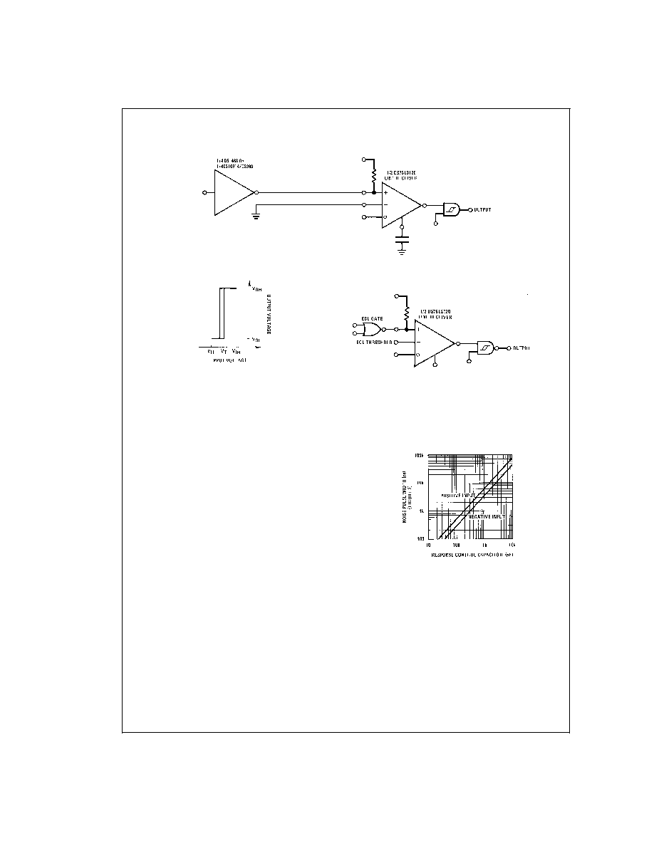
The DS78LS120 may be used as a level translator to inter-
face between
±
12V MOS, ECL, TTL and CMOS. To config-
ure, bias either input to a voltage equal to
1
/
2
the voltage of
the input signal, and the other input to the driving gate.
LINE DRIVERS
Line drivers which will interface with the DS78LS120 are
listed below.
Balanced Drivers
DS26LS31: Quad RS-422 Line Driver, Dual CMOS
DS7830, DS8830: Dual TTL
DS7831, DS8831: Dual TRI-STATE TTL
DS7832, DS8832: Dual TRI-STATE TTL
DS1691A, DS3691: Quad RS-423/Dual RS-422 TTL
DS1692, DS3692: Quad RS-423/Dual TRI-STATE RS-422
TTL
DS3487: Quad TRI-STATE RS-422
Unbalanced Drivers
DS1488: Quad RS-232
DS75150: Dual RS-232
RESPONSE CONTROL AND HYSTERESIS
In unbalanced (RS-232/RS-423) applications it is recom-
mended that the rise time and fall time of the line driver be
controlled to reduce cross-talk. Elimination of switching
noise is accomplished in the DS78LS120 by the 50 mV of
hysteresis incorporated in the output gate. This eliminates
the oscillations which may appear in a line receiver due to
the input signal slowly varying about the threshold level for
extended periods of time.
High frequency noise which is superimposed on the input
signal which may exceed 50 mV can be reduced in ampli-
tude by filtering the device input. On the DS78LS120, a high
impedance response control pin in the input amplifier is
available to filter the input signal without affecting the termi-
nation impedance of the transmission line. Noise pulse width
rejection vs the value of the response control capacitor is
shown in
Figure 1 and Figure 2. This combination of filters
followed by hysteresis will optimize performance in a worse
case noise environment.
Unbalanced Data Transmission
DS007499-6
DS007499-7
Logic Level Translator
DS007499-8
DS007499-9
FIGURE 1. Noise Pulse Width vs
Response Control Capacitor
www.national.com
4

Application Hints
(Continued)
TRANSMISSION LINE TERMINATION
On a transmission line which is electrically long, it is advis-
able to terminate the line in its characteristic impedance to
prevent signal reflection and its associated noise/cross-talk.
A 180
termination resistor is provided in the DS78LS120
line receiver. To use the termination resistor, connect pins 2
and 3 together and pins 13 and 14 together. The 180
resis-
tor provides a good compromise between line reflections,
power dissipation in the driver, and IR drop in the transmis-
sion line. If power dissipation and IR drop are still a concern,
a capacitor may be connected in series with the resistor to
minimize power loss.
The value of the capacitor is recommended to be the line
length (time) divided by 3 times the resistor value. Example:
if the transmission line is 1,000 feet long, (approximately
1000 ns), and the termination resistor value is 180
, the ca-
pacitor value should be 1852 pF. For additional application
details, refer to application notes AN-22 and AN-108.
FAIL-SAFE OPERATION
Communication systems require elements of a system to de-
tect the presence of signals in the transmission lines, and it
is desirable to have the system shut-down in a fail-safe
mode if the transmission line is open or shorted. To facilitate
the detection of input opens or shorts, the DS78LS120 incor-
porates an input threshold voltage offset. This feature will
force the line receiver to a specific logic state if presence of
either fault is a condition.
Given that the receiver input threshold is
±
200 mV, an input
signal greater than
±
200 mV insures the receiver will be in a
specific logic state. When the offset control input (pins 1 and
15) is connected to V
CC
= 5V, the input thresholds are offset
from 200 mV to 700 mV, referred to the non-inverting input,
or -200 mV to -700 mV, referred to the inverting input.
Therefore, if the input is open or shorted, the input will be
greater than the input threshold and the receiver will remain
in a specified logic state.
The input circuit of the receiver consists of a 5k resistor ter-
minated to ground through 120
on both inputs. This net-
work acts as an attenuator, and permits operation with
common-mode input voltages greater than
±
15V. The offset
control input is actually another input to the attenuator, but its
resistor value is 56k. The offset control input is connected to
the inverting input side of the attenuator, and the input volt-
age to the amplifier is the sum of the inverting input plus 0.09
times the voltage on the offset control input. When the offset
control input is connected to 5V the input amplifier will see
V
IN(INVERTING)
+0.45V or V
IN(INVERTING)
+0.9V when the con-
trol input is connected to 10V. The offset control input will not
significantly affect the differential performance of the re-
ceiver over its common-mode operating range, and will not
change the input impedance balance of the receiver.
It is recommended that the receiver be terminated (500
or
less) to insure it will detect an open circuit in the presence of
noise.
The offset control can be used to insure fail-safe operation
for unbalanced interface (RS-423) or for balanced interface
(RS-422) operation.
For unbalanced operation, the receiver would be in an inde-
terminate logic state if the offset control input was open.
Connecting the fail-safe offset pin to 5V, offsets the receiver
threshold to 0.45V. The output is forced to a logic zero state
if the input is open or shorted.
DS007499-10
FIGURE 2.
Unbalanced RS-423 and RS-232 Fail-Safe
DS007499-11
www.national.com
5