 | –≠–ª–µ–∫—Ç—Ä–æ–Ω–Ω—ã–π –∫–æ–º–ø–æ–Ω–µ–Ω—Ç: DS8187 | –°–∫–∞—á–∞—Ç—å:  PDF PDF  ZIP ZIP |
TL F 11220
DS8187
Vacuum
Fluorescent
Display
Driver
June 1992
DS8187 Vacuum Fluorescent Display Driver
General Description
The DS8187 is a vacuum fluorescent display tube driver
This device is implemented in CMOS technology to provide
high voltage output drivers and low power Dimming may be
accomplished by either analog or digital input Autoload ca-
pability is accomplished by connecting the DATA OUT pin to
the LOAD ENABLE input pin with the addition of a start bit
to the input data stream
Features
Y
33 Segment Direct Drive 25
b
0 8 mA and 8
b
2 mA
output drivers
Y
49 steps of dimming mask programmable
Y
Analog or digital input dimming control
Y
DATA OUT pin for cascading
Y
Mask options allow reconfiguring of outputs with
respect to shift register bit position
Y
Autoload or external load capability
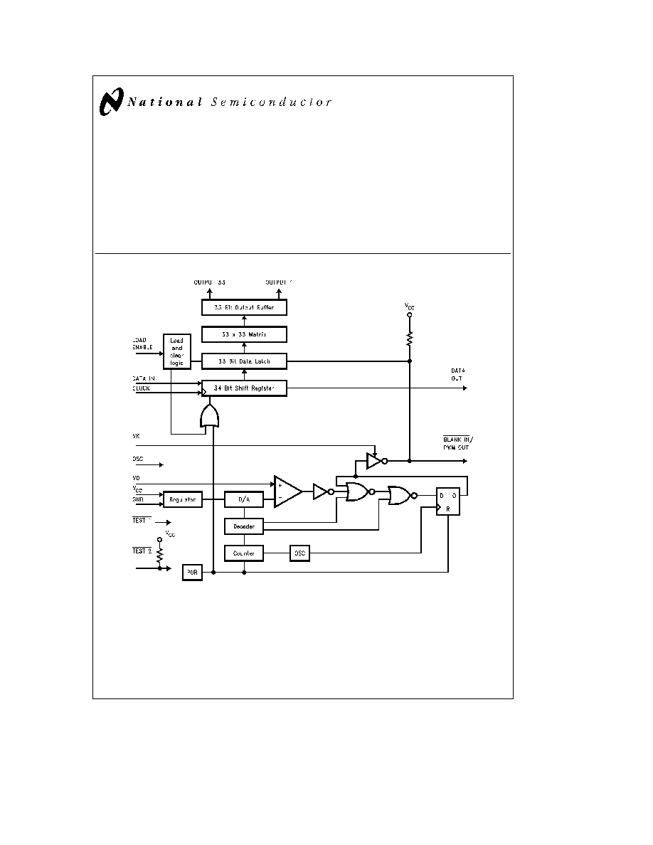
Block Diagram
TL F 11220 ≠ 4
FIGURE 1
C1995 National Semiconductor Corporation
RRD-B30M105 Printed in U S A
Absolute Maximum Ratings
If Military Aerospace specified devices are required
please contact the National Semiconductor Sales
Office Distributors for availability and specifications
Supply Volltage (V
CC
)
b
0 3 to
a
20V
DC Input Voltage (V
IN
)
b
0 3 to VCC
a
0 3V
DC Output Voltage (V
OUT
)
Storage Temperature Range
b
65 to
a
150 C
Lead Temperature (Soldering 10 sec )
260 C
Operating Conditions
Min
Max
Unit
Supply Voltage (V
CC
)
8
18
V
DC Input or Output Voltage
0
V
CC
V
Temperature Range
b
40
a
85
C
Electro-Static Discharge (ESD)
2K
V
Power Dissipation (PD) at 25 C
DIP Board Mount
TBD
DIP Socket Mount
TBD
Typical Values
i
JA DIP Board Mount
TBD C W
i
JA DIP Socket Mount
TBD C W
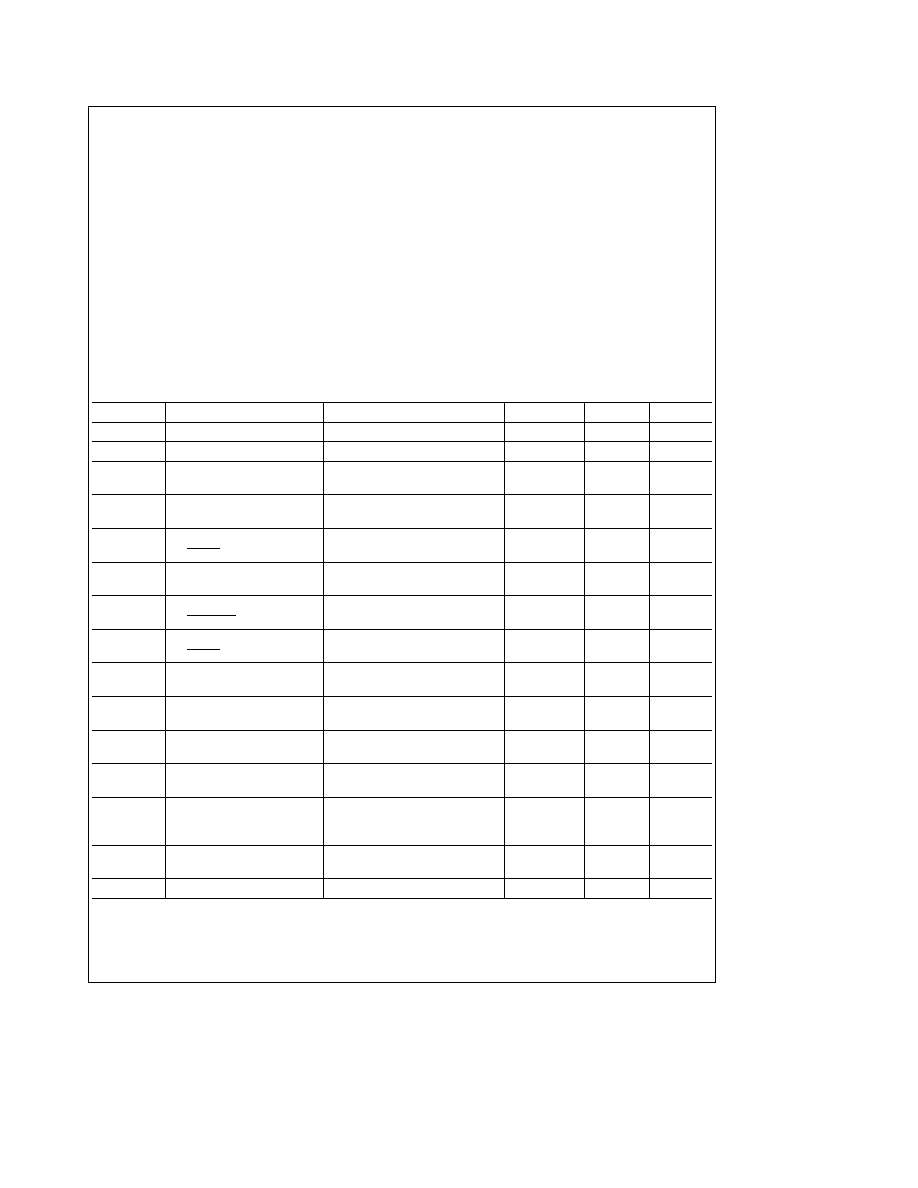
DC Electrical Characteristics
V
CC
e
8V to 18V All voltages referenced to GND unless otherwise specified
Symbol
Parameter
Conditions
Min
Max
Units
V
IH
High Level Input Voltage
3 8
6
V
V
IL
Low Level Input Voltage
0
0 8
V
I
IH1
High Level Input Current
V
IH1
e
5 0V
b
5
5
m
A
(Clock Data In Load VK)
I
IH2
High Level Input Current
V
IH2
e
5 0V T
e
25 C
b
20
10
m
A
(Blank)
I
IH3
High Level Input Current
V
IH3
e
% 0V T
e
25 C
b
100
20
m
A
(TEST2)
I
IL1
Low Level Input Current
V
IL1
e
0V
b
5
5
m
A
(Clock Data In Load VK)
I
IL2
Low Level Input Current
V
IL2
e
0V T
e
25 C
b
125
b
5
m
A
(BLANK IN)
I
IL3
Low Level Input Current
V
IL3
e
0V T
e
25 C
b
700
b
100
m
A
(TEST2)
I
LI
Input Leak Current
V
IN
0V to 6V
b
5
5
m
A
(VD)
V
OH1
High Level Output Voltage
V
CC
e
9 5V I
OH1
e b
0 8 mA
V
CC
b
0 8
V
(Low Current Driver)
V
OH2
High Level Output Voltage
V
CC
e
9 5V I
OH2
e b
2 mA
V
CC
b
0 8
V
(High Current Drive)
V
OH3
High Level Output Voltage
V
CC
e
9 5V I
OH3
e b
200 mA
4
6
V
(DATA OUT PWM OUT)
I
OH3
e b
20 mA
4 5
6
V
V
OL1
Low Level Output Voltage
V
CC
e
9 5V
I
OL1
e
500 mA
2
V
(All Drivers)
I
OL1
e
200 mA
1
V
I
OL1
e
2 mA
0 3
V
V
OL2
Low Level Output Voltage
V
CC
e
9 5V I
OL2
e
200 mA
0 8
V
(DATA OUT PWM OUT)
I
CC
Supply Current
No Load
20
mA
Note 1
Absolute maximum ratings are those values beyond which damage to the device may occur
2

AC Electrical Characteristics
Symbol
Parameter
Conditions
Min
Max
Units
f
C
Clock Frequency
250
kHz
PW
C
Clock Pulse Width
1 3
m
s
t
S
Data Set-Up Time
1
m
s
t
H
Data Hold Time
200
ns
PW
L
Load Pulse Width
1 3
m
s
to
DB
Output Delay from Blank
C
L
e
100 pF
7
m
s
to
DL
Output Delay from Load
C
L
e
100 pF
8
m
s
t
r
Rise Time (All Driver Outputs)
C
L
e
100 pF t
e
20% to 80% of V
CC
5
m
s
t
f
Fall Time (All Driver Outputs)
CL
e
100 pF t
e
80% to 20% of V
CC
5
m
s
Dimming Characteristics
DC Characteristics
Parameter
Conditions
Min
Typ
Max
Units
V
D
Offset Voltage
g
V
D
(3%
a
6%)
g
10
mV
(Note 2)
AC Characteristics
Parameter
Conditions
Min
Typ
Max
Units
Pulse Width Error
No Load (Note 3)
g
100
ns
PWM OUT Frequency
150
250
400
Hz
OSC Frequency
307 2
512
819 2
kHz
Note 2
Reference voltage is 6 1V typical
Note 3
Under the ideal condition of DC parameters
AC Test Conditions
Input Pulse Levels
0 5V to 3 5V
Input Rise and Fall Times
6 ns (10% to 90%)
Propagation Delays Measured at 20% and 80% points
of respective waveforms
3

Timing Waveforms
TL F 11220 ≠ 3
FIGURE 2
4
Functional Description
SHIFT REGISTER OPERATION
Refer to block diagram
Figure 1 while LOAD ENABLE is
low data is entered into the shift register on the rising edge
of the clock The first data bit entered is stored in position
0 the last data bit entered is stored in position
33 A
high voltage level applied to the LOAD ENABLE input trans-
fers the data from the shift register to the data latch The
data is presented to the output drivers through a 33 x 33
matrix This matrix determines shift register output designa-
tion The DS8187 has 34 shift register positions 33 data
latches and 33 output drivers
AUTO LOAD MODE
In this mode the DATA OUT pin is connected to the LOAD
ENABLE pin The data word consists of 34 bits including a
leading start bit(logic 1) On the positive-going-edge of the
34th clock (LOAD ENABLE goes High) data is transferred
to the data latches and the shift register is cleared
DIRECT LOAD MODE
In this mode the DATA OUT pin is not connected to the
LOAD ENABLE pin The LOAD ENABLE pin is controlled
directly by the user When LOAD ENABLE goes High the
contents of the shift register are latched presented to the
output drivers through the 33 x 33 PLA matrix and the shift
register is cleared
DIMMING FUNCTION
When VK is Low the BLANK IN PWM OUT pin functions as
an input blanking signal When BLANK IN PWM is High the
output duty cycle is 100% The duty cycle of a user supplied
signal to this pin will determine the brightness of the output
When VK is High the duty cycle of the output drivers is
controlled by an analog voltage applied to the VD pin
Table I indicates the duty cycle of the output drivers with
respect to the analog voltage applied to VD pin
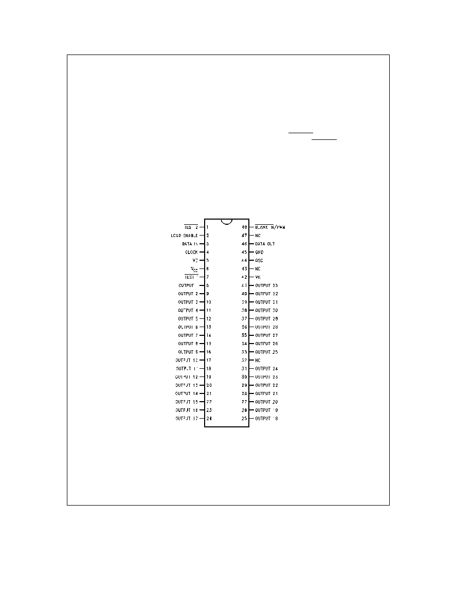
Connection Diagram
Dual-In-Line Package
TL F 11220 ≠ 1
Top View
Order Number DS8187N
See NS Package Number N48A
5