 | –≠–ª–µ–∫—Ç—Ä–æ–Ω–Ω—ã–π –∫–æ–º–ø–æ–Ω–µ–Ω—Ç: DS8614 | –°–∫–∞—á–∞—Ç—å:  PDF PDF  ZIP ZIP |
TL F 5240
DS8615DS8616
130225
MHz
Low
Power
Dual
Modulus
Prescalers
July 1992
DS8615 DS8616 130 225 MHz
Low Power Dual Modulus Prescalers
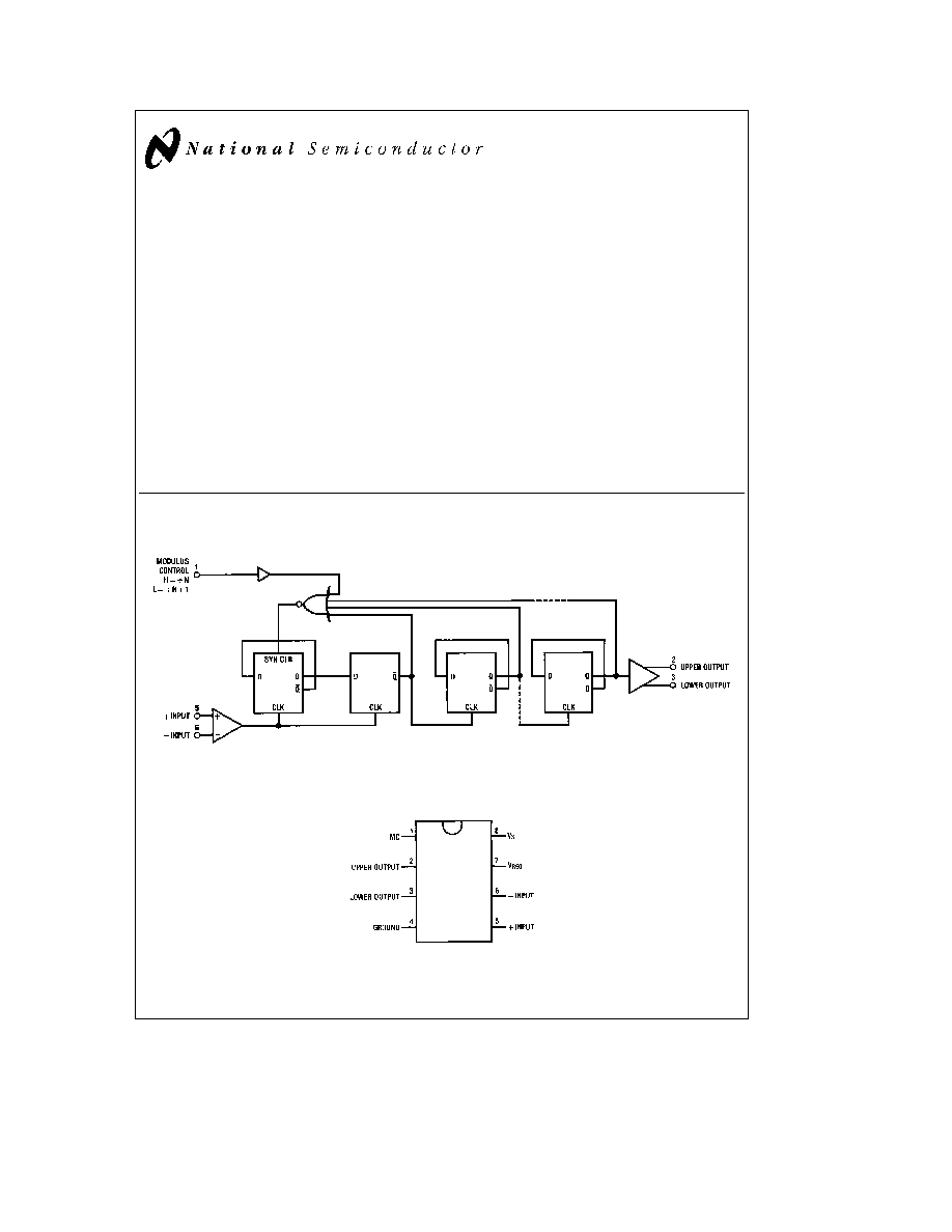
General Description
The DS8615 series products are low power dual modulus
prescalers which divide by 32 33 and 40 41 respectively
The modulus control (MC) input selects division by N when
at a high TTL level and division by N
a
1 when at a low TTL
level The clock inputs are buffered providing 40 100
mVrms input sensitivity The two outputs provide the user
the option to wire either a totem-pole or open-collector out-
put structure Additionally the user can wire a resistor be-
tween the two output pins to minimize edge transition emis-
sions The outputs are designed to drive positive edge trig-
gered PLLs These products can be operated from either an
unregulated 5 5V to 13 5V source or regulated 5V
g
10%
source Unregulated operation is obtained by connecting V
S
to the source with V
REG
open Regulated operation is ob-
tained by connecting both V
S
and V
REG
to the supply
source
The device can be used in phase-locked loop applications
such as FM radio or other communications bands to pre-
scale the input frequency down to a more usable level A
digital frequency display system can also be derived sepa-
rately or in conjunction with a phase-locked loop and it can
extend the useful range of many inexpensive frequency
counters to 225 MHz
Features
Y
Input frequency 130 MHz (-4) 225 MHz (-2)
Y
Low power 10 mA (-4 -2)
Y
Input sensitivity 100 mVrms (-4) 40 mVrms (-2)
Y
Pin compatible with Motorola MC12015-16 prescalers
Y
Unregulated regulated power supply option
Logic and Connection Diagrams
Generalized
d
N N
a
1
TL F 5240 ≠ 1
Dual-In-Line Package
TL F 5240 ≠ 2
Top View
Order Number DS8615N or DS8616N (-4 -2)
See NS Package Number N08E
C1995 National Semiconductor Corporation
RRD-B30M105 Printed in U S A
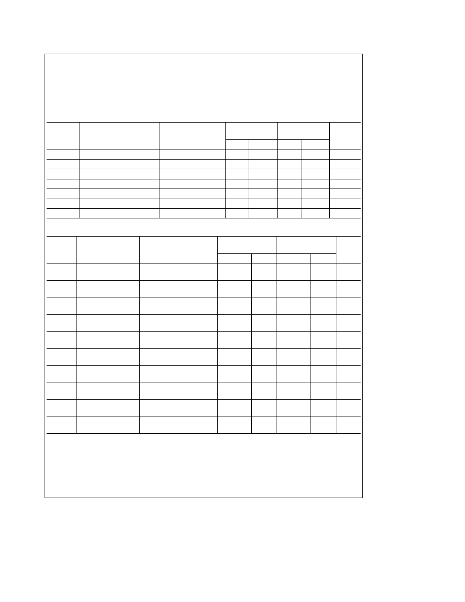
Absolute Maximum Ratings
(Note 1)
If Military Aerospace specified devices are required
please contact the National Semiconductor Sales
Office Distributors for availability and specifications
V
S
Unregulated Supply Voltage
15V
V
REG
Regulated Supply Voltage
7V
Modulus Control Input Voltage
7V
Open-Collector Output Voltage
7V
Operating Free Air Temperature Range
b
30 C to
a
70 C
Storage Temperature Range
b
65 C to
a
150 C
Recommended Operating Conditions
Symbol
Parameter
Conditions
DS8615-4
DS8615-2
DS8616-4
DS8616-2
Units
Min
Max
Min
Max
V
S
Unregulated Supply Voltage
V
REG
e
Open
6 8
13 5
5 5
13 5
V
V
REG
Regulated Supply Voltage
V
S
and V
REG
Shorted
4 5
5 5
4 5
5 5
V
f
MAX
Toggle Frequency
V
IN
e
100 mVrms
20
130
225
MHz
V
IN
Input Signal Amplitude
100
300
40
300
mVrms
V
SLW
Slew Rate
20
20
V ms
I
OH
High Level Output Current
b
400
b
400
m
A
I
OL
Low Level Output Current
2 0
2 0
mA
DC Electrical Characteristics
(Notes 2 and 3)
DS8615-4
DS8615-2
Symbol
Parameter
Conditions
DS8616-4
DS8616-2
Units
Min
Max
Min
Max
V
IH
High Level MC Input
V
S
e
13 5V V
REG
e
Open
2 0
2 0
V
Voltage
V
IL
Low Level MC Input
V
REG
e
V
S
e
4 5V
0 8
0 8
V
Voltage
V
OH
High Level Output
I
OH
e b
0 4 mA
V
REG
b
2
V
REG
b
2
V
Voltage
Pins 2 and 3 Shorted
I
CEX
Open-Collector High
Lower Output
e
5 5V
100
100
m
A
Level Output
V
OL
Low Level Output
V
REG
e
4 5V I
OL
e
2 mA
0 5
0 5
V
Voltage
I
I
Max MC Input Current
V
S
e
13 5V V
REG
e
Open
100
100
m
A
V
IH
e
7V
I
IH
High Level MC Input
V
REG
e
4 5V V
IH
e
2 7V
20
20
m
A
Current
I
IL
Low Level MC Input
V
S
e
13 5V V
REG
e
Open
b
200
b
200
m
A
Current
V
IL
e
0 4V
I
S
Supply Current
V
S
e
13 5V V
REG
e
Open
10
10
mA
Unregulated Mode
I
REG
Supply Current
V
S
e
V
REG
e
5 5V
10
10
mA
Regulated Mode
Note 1
``Absolute Maximum Ratings'' are those values beyond which the safety of the device cannot be guaranteed They are not meant to imply that the device
should be operated at these limits The table of ``Electrical Characteristics'' provides conditions for actual device operation
Note 2
Unless otherwise specified Min Max limits apply across the
b
30 C to
a
70 C range
Note 3
All current into device pins shown as positive out of device pins as negative all voltages referenced to ground unless otherwise noted All values shown as
Max or Min on absolute value basis
2
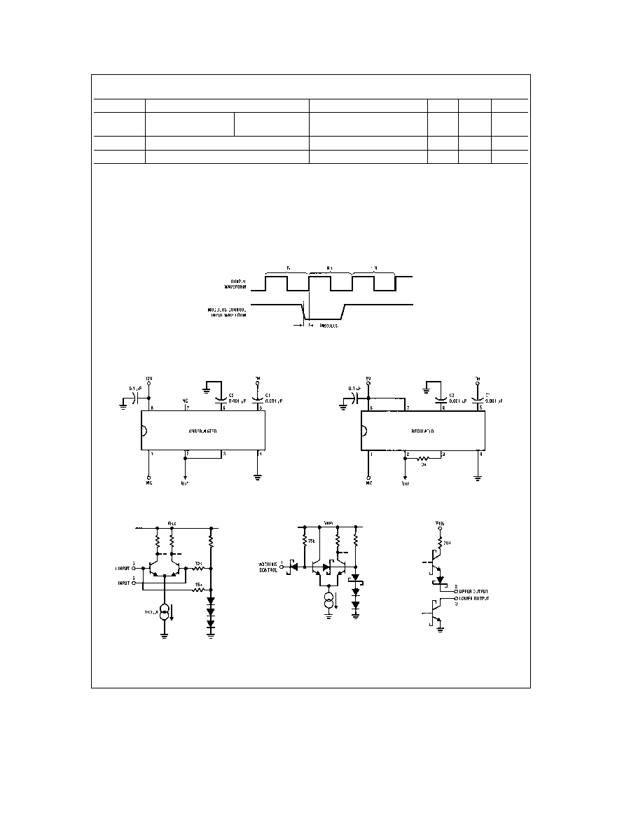
AC Electrical Characteristics
V
CC
e
5V
g
10% T
A
e b
30 C to
a
70 C
Symbol
Parameter
Conditions
Min
Max
Units
t
MODULUS
Modulus Set-Up Time
DS8615 DS8616
65
ns
(Notes 4 and 5)
R
IN
AC Input Resistance
V
IN
e
100 MHz and 50 mVrms
1 0
kX
C
IN
Input Capacitance
V
IN
e
100 MHz and 50 mVrms
3
10
pF
Note 1
``Absolute Maximum Ratings'' are those values beyond which the safety of the device cannot be guaranteed Except for ``Operating Temperature Range''
they are not meant to imply that the devices should be operated at these limits The table of ``Electrical Characteristics'' provides conditions for actual device
operation
Note 2
Unless otherwise specified min max limits apply across the
b
30 C to
a
70 C temperature range
Note 3
All currents into device pins are shown as positive out of device pins as negative all voltages referenced to ground unless otherwise noted All values
shown as max or min on absolute value basis
Note 4
t
MODULUS
e
the period of time the modulus control level must be defined prior to the positive transition of the prescaler output to ensure proper modulus
selection
Note 5
See Timing Diagrams
Timing Diagram
TL F 5240 ≠ 3
The logical state of the modulus control input just prior to the output's rising edge will determine the modulus ratio of the device
immediately following that rising edge The pulse width difference of N and N
a
1 operation occurs during the output
e
HI conditions
Typical Applications
TL F 5240 ≠ 4
TL F 5240 ≠ 5
Schematic Diagrams
TL F 5240 ≠ 6
TL F 5240 ≠ 7
TL F 5240 ≠ 8
3

Application Hints
OPERATING NOTES
The signal source is usually capacitively coupled to the in-
put At higher frequencies a 0 001 mF input capacitor (C1) is
usually sufficient with larger values used at the lower fre-
quencies If the input signal is likely to be interrupted it may
be desirable to connect a 100 kX resistor between one in-
put and ground to stabilize the device In the single-ended
mode it is preferable to connect the resistor to the unused
input In the differential mode the resistor can be connected
to either input The addition of the 100 kX pulldown resistor
causes a loss of input sensitivity but prevents circuit oscilla-
tions under no signal (open circuit) conditions In addition in
the single ended mode a capacitor of 0 001 mF (C2) should
be connected between the unused input and the ground
plane to provide a good high frequency bypass The capaci-
tor should be made larger for lower frequencies
The input waveform may be sinusoidal but below about
20 MHz the operation of the circuit becomes dependent on
the slew rate of the input rather than amplitude A square
wave input with a slew rate of greater than 20 V ms will
permit correct operation down to lower frequencies provid-
ed the proper input coupling capacitor is provided
For regulated mode operation connect V
S
to V
REG
to en-
sure proper operation (see Typical Application diagram)
4

Physical Dimensions
inches (millimeters)
Molded Dual-In-Line Package (M)
Order Number DS8614M-4 DS8615M-4 DS8616M-4 or DS8617M-4
NS Package Number M08A
5