 | –≠–ª–µ–∫—Ç—Ä–æ–Ω–Ω—ã–π –∫–æ–º–ø–æ–Ω–µ–Ω—Ç: DS8835N | –°–∫–∞—á–∞—Ç—å:  PDF PDF  ZIP ZIP |
TL F 5808
DS7833DS8833DS7835DS8835
Quad
TRI-STATE
Bus
Transceivers
February 1996
DS7833 DS8833 DS7835 DS8835
Quad TRI-STATE
Bus Transceivers
General Description
This family of TRI-STATE bus transceivers offers extreme
versatility in bus organized data transmission systems The
data bus may be unterminated or terminated DC or AC at
one or both ends Drivers in the third (high impedance) state
load the data bus with a negligible leakage current The
receiver input current is low allowing at least 100 driver re-
ceiver pairs to utilize a single bus The bus loading is un-
changed when V
CC
e
0V The receiver incorporates hyster-
esis to provide greater noise immunity All devices utilize a
high current TRI-STATE output driver
The DS7833
DS8833 and DS7835 DS8835 employ TRI-STATE outputs
on the receiver also
The DS7833 DS8833 are non-inverting quad transceivers
with a common inverter driver disable control and common
inverter receiver disable control
The DS7835 DS8835 are inverting quad transceivers with a
common inverter driver disable control and a common in-
verter receiver disable control
Features
Y
Receiver hysteresis
400 mV typ
Y
Receiver noise immunity
1 4V typ
Y
Bus terminal current for
80 mA max
normal V
CC
or V
CC
e
0V
Y
Receivers
Sink
16 mA at 0 4V max
Source
2 0 mA (Mil) at 2 4V min
5 2 mA (Com) at 2 4V min
Y
Drivers
Sink
50 mA at 0 5V max
32 mA at 0 4V max
Source
10 4 mA (Com) at 2 4V min
5 2 mA (Mil) at 2 4V min
Y
Drivers have TRI-STATE outputs
Y
DS7833 DS8833 DS7835 DS8835 receivers have
TRI-STATE outputs
Y
Capable of driving 100X DC
terminated buses
Y
Compatible with Series 54 74
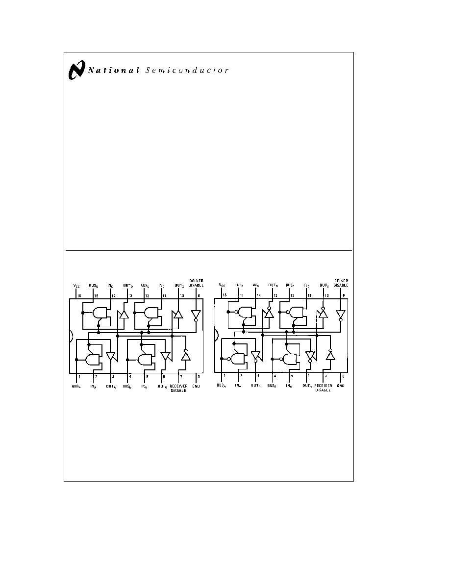
Connection Diagram
Dual-In-Line Package
TL F 5808 ≠ 1
Top View
Order Number DS7833J or DS8833N
See NS Package Number J16A or N16A
Dual-In-Line Package
TL F 5808 ≠ 2
Top View
Order Number DS7835J or DS8835N
See NS Package Number J16A or N16A
TRI-STATE
is a registered trademark of National Semiconductor Corp
C1996 National Semiconductor Corporation
RRD-B30M36 Printed in U S A
http
www national com
Absolute Maximum Ratings
(Note 1)
If Military Aerospace specified devices are required
please contact the National Semiconductor Sales
Office Distributors for availability and specifications
Supply Voltage
7 0V
Input Voltage
5 5V
Output Voltage
5 5V
Storage Temperature
b
65 C to
a
150 C
Maximum Power Dissipation at 25 C
Cavity Package
1509 mW
Molded Package
1476 mW
Lead Temperature (Soldering 4 sec )
260 C
Derate cavity package 10 1 mW C above 25 C derate molded package
11 8 mW C above 25 C
Operating Conditions
Min
Max
Units
Supply Voltage V
CC
DS7833 DS7835
4 5
5 5
V
DS8833 DS8835
4 75
5 25
V
Temperature (T
A
)
DS7833 DS7835
b
55
a
125
C
DS8833 DS8835
0
a
70
C
Electrical Characteristics
(Notes 2 and 3)
Symbol
Parameter
Conditions
Min
Typ
Max
Units
DISABLE DRIVER INPUT
V
IH
High Level Input Voltages
V
CC
e
Min
2 0
V
V
IL
Low Level Input Voltage
V
CC
e
Min
DS7833 DS8833 DS8835
0 8
V
DS7835
0 7
I
IH
High Level Input Current
V
CC
e
Max
V
IN
e
2 4V
40
m
A
V
IN
e
5 5V
1 0
mA
I
IL
Low Level Input Current
V
CC
e
Max V
IN
e
0 4V
b
1 0
b
1 6
mA
V
CL
Input Clamp Diode
V
CC
e
5 0V I
IN
e b
12 mA T
A
e
25 C
b
0 8
b
1 5
V
I
IT
Driver Low Level Disabled
Driver Disable Input
e
2 0V V
IN
e
0 4V
b
40
m
A
Input Current
RECEIVER INPUT BUS OUTPUT
V
TH
High Level Threshold Voltage
DS7833 DS7835
1 4
1 75
2 1
V
DS8833 DS8835
1 5
1 75
2 0
V
V
TL
Low Level Threshold Voltage
DS7833 DS7835
0 8
1 35
1 6
V
DS8833 DS8835
0 8
1 35
1 5
V
I
S
Bus Current Output Disabled
V
BUS
e
4 0V
V
CC
e
Max
25
80
m
A
or High
V
CC
e
0V
5 0
80
m
A
V
CC
e
Max V
BUS
e
0 4V
b
2 0
b
40
m
A
V
OH
Logic ``1'' Output Voltage
V
CC
e
Min
I
OUT
e b
5 2 mA
DS7833 DS7835
2 4
2 75
V
I
OUT
e b
10 4 mA DS8833 DS8835
2 4
2 75
V
V
OL
Logic ``0'' Output Voltage
V
CC
e
Min
I
OUT
e
50 mA
0 28
0 5
V
I
OUT
e
32 mA
0 4
V
I
OS
Output Short Circuit Current
V
CC
e
Max (Note 4)
b
40
b
62
b
120
mA
RECEIVER OUTPUT
V
OH
Logic ``1'' Output Voltage
V
CC
e
Min
I
OUT
e b
2 0 mA
DS7833 DS7835
2 4
3 0
V
I
OUT
e b
5 2 mA
DS8833 DS8835
2 4
2 9
V
V
OL
Logic ``0'' Output Voltage
V
CC
e
Min I
OUT
e
16 mA
0 22
0 4
V
I
OT
Output Disabled Current
V
CC
e
Max Disable V
OUT
e
2 4V
40
m
A
Inputs
e
2 0V
V
OUT
e
0 4V
b
40
m
A
http
www national com
2
Electrical Characteristics
(Notes 2 and 3) (Continued)
Symbol
Parameter
Conditions
Min
Typ
Max
Units
RECEIVER OUTPUT
(Continued)
I
OS
Output Short Circuit Current
V
CC
e
Max (Note 4)
DS7833 DS7835
28
b
40
b
70
mA
DS8833 DS8835
b
30
b
70
mA
I
CC
Supply Current
V
CC
e
Max
DS7833 DS8833
84
116
mA
DS7835 DS8835
75
95
mA
Note 1
``Absolute Maximum Ratings'' are those values beyond which the safety of the device cannot be guaranteed Except for ``Operating Temperature Range''
they are not meant to imply that the devices should be operated at these limits The table of ``Electrical Characteristics'' provides conditions for actual device
operation
Note 2
Unless otherwise specified min max limits apply across the
b
55 C to
a
125 C temperature range for the DS7833 DS7835 and across the 0 C to
a
70 C
range for the DS8833 DS8835 All typicals are given for V
CC
e
5 0V and T
A
e
25 C
Note 3
All currents into device pins shown as positive out of device pins as negative all voltages referenced to ground unless otherwise noted All values shown
as max or min on absolute value basis
Note 4
Only one output at a time should be shorted
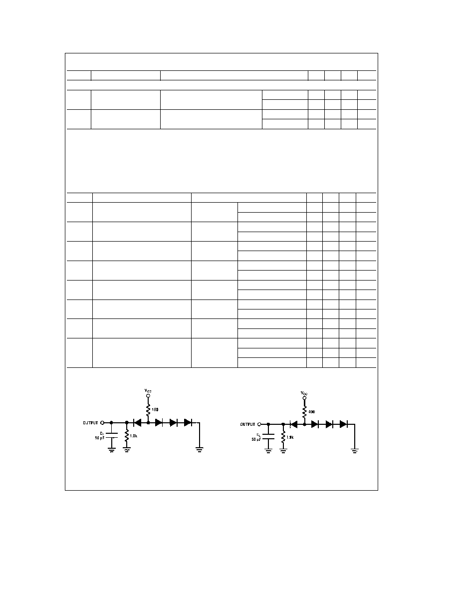
Switching Characteristics
V
CC
e
5 0V T
A
e
25 C
Symbol
Parameter
Conditions
Min
Typ
Max
Units
t
pd0
Propagation Delay to a Logic ``0''
(Figure 1)
DS7833 DS8833
14
30
ns
from Input to Bus
DS7835 DS8835
10
20
ns
t
pd1
Propagation Delay to a Logic ``1''
(Figure 1)
DS7833 DS8833
14
30
ns
from Input to Bus
DS7835 DS8835
11
30
ns
t
pd0
Propagation Delay to a Logic ``0''
(Figure 2)
DS7833 DS8833
24
45
ns
from Bus to Input
DS7835 DS8835
16
35
ns
t
pd1
Propagation Delay to a Logic ``1''
(Figure 2)
DS7833 DS8833
12
30
ns
from Bus to Input
DS7835 DS8835
18
30
ns
t
PHZ
Delay from Disable Input to High
C
L
e
5 0 pF
Driver
8 0
20
ns
Impedance State (from Logic ``1'' Level)
(
Figures 1 and 2 )
Receiver
6 0
15
ns
t
PLZ
Delay from Disable Input to High
C
L
e
5 0 pF
Driver
20
35
ns
Impedance State (from Logic ``0'' Level)
(
Figures 1 and 2 )
Receiver
13
25
ns
t
PZH
Delay from Disable Input to Logic
C
L
e
5 0 pF
Driver
24
40
ns
``1'' Level (from High Impedance State)
(
Figures 1 and 2 )
Receiver
16
35
ns
t
PZL
Delay from Disable Input to Logic
C
L
e
5 0 pF
Driver
19
35
ns
``0'' Level (from High Impedance State)
(
Figures 1 and 2 )
Receiver DS7833 DS8833
15
30
ns
Receiver DS7835 DS8835
33
50
ns
AC Test Circuits
TL F 5808 ≠ 3
FIGURE 1 Driver Output Load
TL F 5808 ≠ 4
FIGURE 2 Receiver Output Load
http
www national com
3
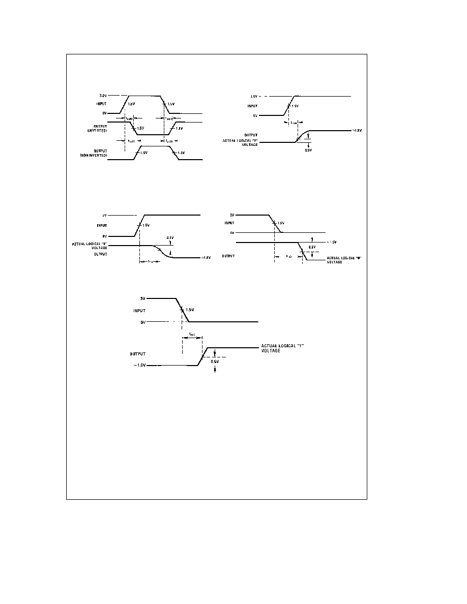
Switching Time Waveforms
t
pd1
t
pd0
TL F 5808 ≠ 5
f
e
1 MHz
t
r
e
t
f
s
10 ns (10% to 90%)
DUTY CYCLE
e
50%
t
PLZ
TL F 5808 ≠ 6
t
PHZ
TL F 5808 ≠ 7
t
PZL
TL F 5808 ≠ 8
t
PZH
TL F 5808 ≠ 9
http
www national com
4
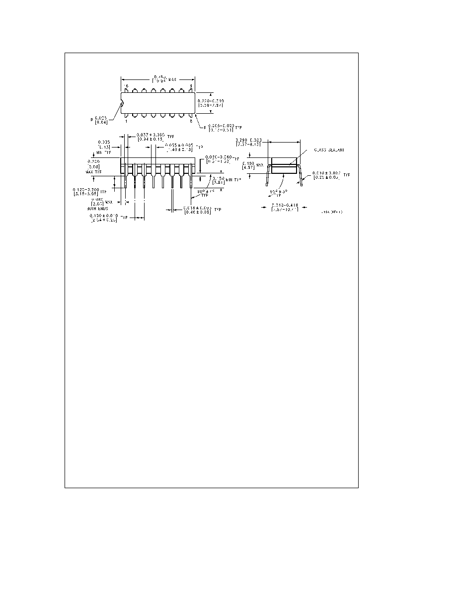
Physical Dimensions
inches (millimeters)
Ceramic Dual-In-Line Package (J)
Order Number DS7833J or DS7835J
NS Package Number J16A
http
www national com
5