TL F 5847
DS8884A
High
Voltage
Cathode
DecoderDriver
May 1986
DS8884A High Voltage Cathode Decoder Driver
General Description
The DS8884A is designed to decode four lines of BCD input
and drive seven-segment digits of gas-filled readout dis-
plays
All outputs consist of switchable and programmable current
sinks which provide constant current to the tube cathodes
even with high tube anode supply tolerance Output currents
may be varied over the 0 2 mA to 1 2 mA range for multiplex
operation The output current is adjusted by connecting an
external program resistor (R
P
) from V
CC
to the program in-
put in accordance with the programming curve Unused out-
puts must be tied to V
CC
Features
Y
Usable with AC or DC input coupling
Y
Current sink outputs
Y
High output breakdown voltage
Y
Low input load current
Y
Intended for multiplex operation
Y
Input pullups increase noise immunity
Y
Comma d pt drive
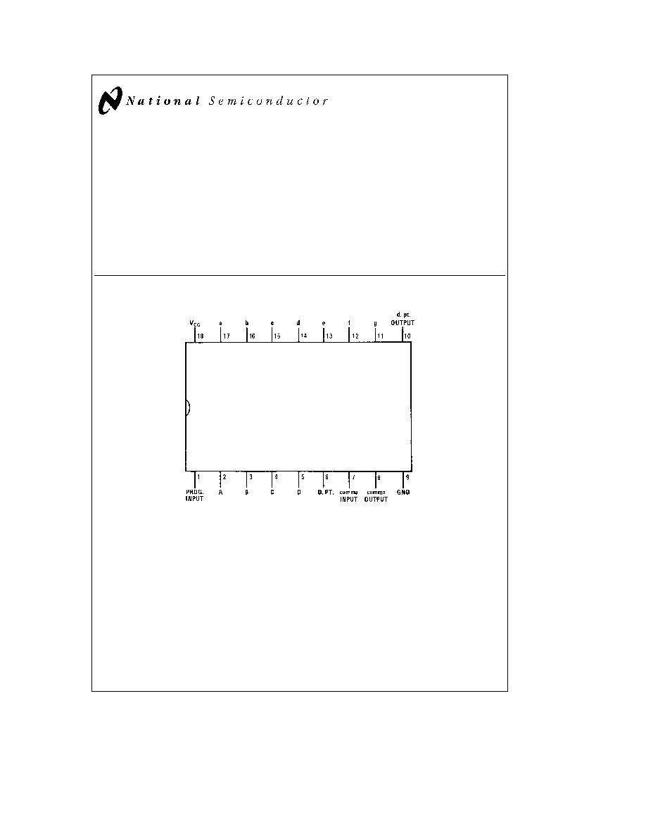
Connection Diagram
Dual-In-Line Package
TL F 5847 � 2
Top View
Order Number DS8884AN
See NS Package Number N18A
C1995 National Semiconductor Corporation
RRD-B30M105 Printed in U S A
Absolute Maximum Ratings
(Note 1)
If Military Aerospace specified devices are required
please contact the National Semiconductor Sales
Office Distributors for availability and specifications
V
CC
7V
Input Voltage (Note 4)
V
CC
Segment Output Voltage
80V
Power Dissipation
600 mW
Transient Segment Output Current
(Note 5)
50 mA
Storage Temperature Range
b
65 C to
a
150 C
Maximum Power Dissipation at 25 C
Molded Package
1714 mW
Derate molded package 13 71 mW C above 25 C
Operating Conditions
Min
Max
Units
Supply Voltage (V
CC
)
4 75
5 25
V
Temperature (T
A
)
0
a
70
C
Electrical Characteristics
(Notes 2 and 3)
Symbol
Parameter
Conditions
Min
Max
Units
V
IH
Logical ``1'' Input Voltage
V
CC
e
4 75V
2 0
V
V
IL
Logical ``0'' Input Voltage
V
CC
e
4 75V
1 0
V
I
IH
Logical ``1'' Input Current
V
CC
e
5 25V V
IN
e
2 4V
15
m
A
I
IL
Logical ``0'' Input Current
V
CC
e
5 25V V
IN
e
0 4V
b
250
m
A
I
CC
Power Supply Current
V
CC
e
5 25V R
P
e
2 8k All Inputs
e
5V
40
mA
V
Ia
Positive Input Clamp Voltage
V
CC
e
4 75V I
IN
e
1 mA
5 0
V
V
Ib
Negative Input Clamp Voltage
V
CC
e
5V I
IN
e b
12 mA T
A
e
25 C
b
1 5
V
D
I
O
SEGMENT OUTPUTS
All Outputs
e
50V I
OUT
b
e
Ref All Outputs
0 9
1 1
``ON'' Current Ratio
I
b ON
Output b ``ON'' Current
V
CC
e
5V V
OUT
b
e
50V
R
P
e
18 1k
0 15
0 25
mA
T
A
e
25 C
R
P
e
7 03k
0 45
0 55
mA
R
P
e
3 40k
0 90
1 10
mA
R
P
e
2 80k
1 08
1 32
mA
I
CEX
Output Leakage Current
V
OUT
e
75V
5
m
A
V
BR
Output Breakdown Voltage
I
OUT
e
250 mA
80
V
t
pd
Propagation Delay of Any
V
CC
e
5V T
A
e
25 C
10
m
s
Input to Segment Output
Note 1
``Absolute Maximum Ratings'' are those values beyond which the safety of the device cannot be guaranteed They are not meant to imply that the devices
should be operated at these limits The table of ``Electrical Characteristics'' provides conditions for actual device operation
Note 2
Unless otherwise specified min max limits apply across the 0 C to
a
70 C temperature range for the DS8884A All typical values are for T
A
e
25 C and
V
CC
e
5V
Note 3
All currents into device pins shown as positive out of device pins as negative all voltages referenced to ground unless otherwise noted All values shown
as max or min on absolute value basis
Note 4
This limit can be higher for a current limiting voltage source
Note 5
In all applications transient segment output current must be limited to 50 mA This may be accomplished in DC applications by connecting a 2 2k resistor
from the anode-supply filter capacitor to the display anode or by current limiting the anode driver in multiplex applications
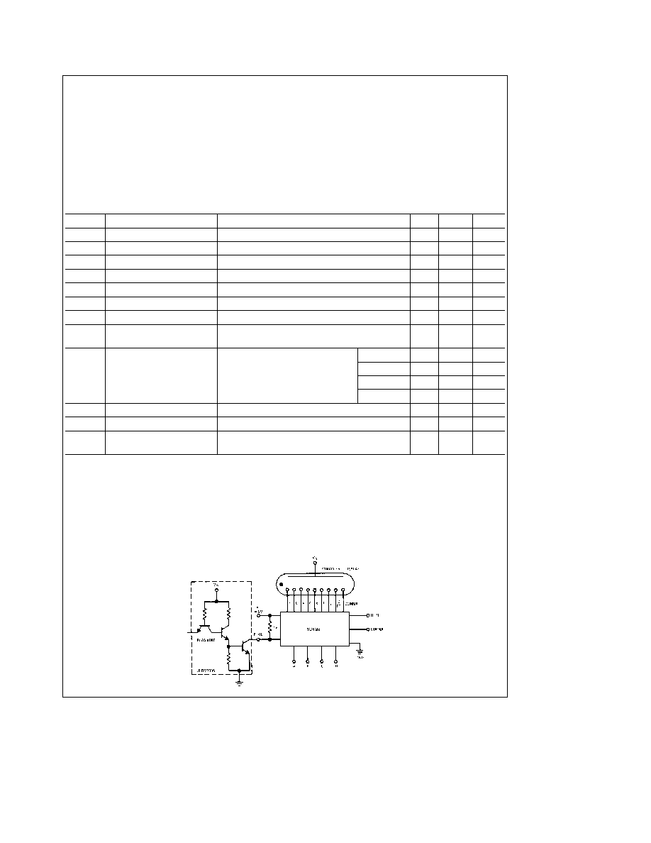
Typical Application
TL F 5847 � 4
2
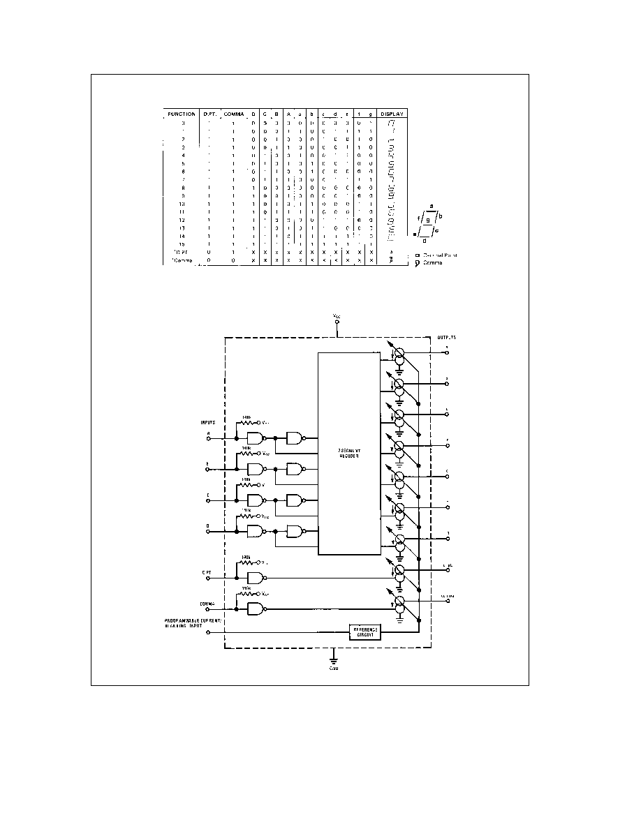
Truth Table
TL F 5847 � 3
Decimal point and comma can be displayed with or without any numeral
Logic Diagram
TL F 5847 � 1
3

DS8884A
High
Voltage
Cathode
DecoderDriver
Physical Dimensions
inches (millimeters)
Molded Dual-In-Line Package (N)
Order Number DS8884AN
NS Package Number N18A
LIFE SUPPORT POLICY
NATIONAL'S PRODUCTS ARE NOT AUTHORIZED FOR USE AS CRITICAL COMPONENTS IN LIFE SUPPORT
DEVICES OR SYSTEMS WITHOUT THE EXPRESS WRITTEN APPROVAL OF THE PRESIDENT OF NATIONAL
SEMICONDUCTOR CORPORATION As used herein
1 Life support devices or systems are devices or
2 A critical component is any component of a life
systems which (a) are intended for surgical implant
support device or system whose failure to perform can
into the body or (b) support or sustain life and whose
be reasonably expected to cause the failure of the life
failure to perform when properly used in accordance
support device or system or to affect its safety or
with instructions for use provided in the labeling can
effectiveness
be reasonably expected to result in a significant injury
to the user
National Semiconductor
National Semiconductor
National Semiconductor
National Semiconductor
Corporation
Europe
Hong Kong Ltd
Japan Ltd
1111 West Bardin Road
Fax (a49) 0-180-530 85 86
13th Floor Straight Block
Tel 81-043-299-2309
Arlington TX 76017
Email cnjwge tevm2 nsc com
Ocean Centre 5 Canton Rd
Fax 81-043-299-2408
Tel 1(800) 272-9959
Deutsch Tel (a49) 0-180-530 85 85
Tsimshatsui Kowloon
Fax 1(800) 737-7018
English
Tel (a49) 0-180-532 78 32
Hong Kong
Fran ais Tel (a49) 0-180-532 93 58
Tel (852) 2737-1600
Italiano
Tel (a49) 0-180-534 16 80
Fax (852) 2736-9960
National does not assume any responsibility for use of any circuitry described no circuit patent licenses are implied and National reserves the right at any time without notice to change said circuitry and specifications