 | –≠–ª–µ–∫—Ç—Ä–æ–Ω–Ω—ã–π –∫–æ–º–ø–æ–Ω–µ–Ω—Ç: DS8907 | –°–∫–∞—á–∞—Ç—å:  PDF PDF  ZIP ZIP |

TL F 7511
DS8907
AMFM
Digital
Phase-Locked
Loop
Frequency
Synthesizer
July 1986
DS8907 AM FM Digital
Phase-Locked Loop Frequency Synthesizer
General Description
The DS8907 is a PLL synthesizer designed specifically for
use in AM FM radios It contains the reference oscillator a
phase comparator a charge pump a 120 MHz ECL I
2
L
dual modulus programmable divider and an 18-bit shift reg-
ister latch for serial data entry The device is designed to
operate with a serial data controller generating the neces-
sary division codes for each frequency and logic state infor-
mation for radio function inputs outputs
The Colpitts reference oscillator for the PLL operates at
4 MHz A chain of dividers is used to generate a 500 kHz
clock signal for the external controller Additional dividers
generate a 25 kHz reference signal for FM and a 10 kHz
reference signal for AM One of these reference signals is
selected by the data from the controller for use by the
phase comparator
Data is transferred between the frequency synthesizer and
the controller via a 3 wire bus system This consists of a
data input line an enable line and a clock line When the
enable line is low data can be shifted from the controller
into the frequency synthesizer When the enable line is tran-
sitioned from low to high data entry is disabled and data
present in the shift register is latched
From the controller 20-bit data stream the first 2 bits ad-
dress the device permitting other devices to share the same
bus Of the remaining 18-bit data word the next 13 bits are
used for the PLL divide code The remaining 5 bits are con-
nected via latches to output pins These 5 bits can be used
to drive radio functions such as gain mute FM AM and
stereo only These outputs are open collector Bit 16 is used
internally to select the AM or FM local oscillator input and to
select between the 10 kHz and 25 kHz reference A high
level at bit 16 indicates FM and a low level indicates AM
The PLL consists of a 13-bit programmable I
2
L divider an
ECL phase comparator an ECL dual modulus (p p
a
1) pre-
scaler and a high speed charge pump The programma-
ble divider divides by (N
a
1) N being the number loaded
into the shift register (bits 1 ≠ 13 after address) It is clocked
by the AM input via an ECL
d
prescaler or through a
d
prescaler from the FM input The AM input will work
at frequencies up to 15 MHz while the FM input works up to
120 MHz The AM band is tuned with a frequency resolution
of 10 kHz and the FM band is tuned with a resolution of
25 kHz The buffered AM and FM inputs are self biased and
can be driven directly by the VCO through a capacitor The
ECL phase comparator produces very accurate resolution
of the phase difference between the input signal and the
reference oscillator The high speed charge pump consists
of a switchable constant current source (
b
0 3 mA) and a
switchable constant current sink (
a
0 3 mA) If the VCO fre-
quency is low the charge pump will source current and sink
current if the VCO frequency is high When using an AFC
the charge pump output may be forced into TRI-STATE
by
applying a low level to the charge pump enable input
A separate V
CCM
pin (typically drawing 1 5 mA) powers the
oscillator and reference chain to provide controller clocking
frequencies when the balance of the PLL is powered down
Features
Y
Uses inexpensive 4 MHz reference crystal
Y
F
IN
capability greater than 120 MHz allows direct syn-
thesis at FM frequencies
Y
FM resolution of 25 kHz allows usage of 10 7 MHz ce-
ramic filter distribution
Y
Serial data entry for simplified control
Y
50 Hz output for ``time-of-day'' reference driven from
separate low power V
CCM
Y
5-open collector buffered outputs for controlling various
radio functions
Y
Separate AM and FM inputs AM input has 15 mV (typi-
cal) hysteresis
Dual-In-Line Package
Connection Diagram
Order Number DS8907N
See NS Package Number
N20A
TL F 7511 ≠ 1
Top View
TRI-STATE
is a registered trademark of National Semiconductor Corporation
C1995 National Semiconductor Corporation
RRD-B30M105 Printed in U S A
Absolute Maximum Ratings
(Note 1)
If Military Aerospace specified devices are required
please contact the National Semiconductor Sales
Office Distributors for availability and specifications
Supply Voltage
(V
CC1
)
7V
(V
CCM
)
7V
Input Voltage
7V
Output Voltage
7V
Storage Temperature Range
b
65 C to
a
150 C
Lead Temperature (Soldering 4 sec )
260 C
Operating Conditions
Min
Max
Units
Supply Voltage V
CC
V
CC1
4 75
5 25
V
V
CCM
4 5
6 0
V
Temperature T
A
0
70
C
DC Electrical Characteristics
(Notes 2 and 3)
Symbol
Parameter
Conditions
Min
Typ
Max
Units
V
IH
Logical ``1'' Input Voltage
2 1
V
I
IH
Logical ``1'' Input Current
V
IN
e
2 7V
0
10
m
A
V
IL
Logical ``0'' Input Voltage
0 7
V
I
IL
Logical ``0'' Input Current
Data Clock and ENABLE Inputs V
IN
e
0V
b
5
b
25
m
A
I
IL
Logical ``0'' Input Current
Charge Pump Enable V
IN
e
0V
b
250
b
450
m
A
I
OH
Logical ``1'' Output Current
V
OH
e
5 25V
50
m
A
All Bit Outputs 50 Hz Output
500 kHz Output
V
OH
e
2 4V V
CCM
e
4 5V
b
250
m
A
V
OL
Logical ``0'' Output Voltage
I
OL
e
5 mA
0 5
V
All Bit Outputs
50 Hz Output 500 Hz Output
I
OL
e
250 mA
0 5
V
I
CC1
Supply Current (V
CC1
)
All Bits Outputs High
90
160
mA
I
CCM(STANDBY)
V
CCM
Supply Current
V
CCM
e
6 0V All Other Pins Open
1 5
4 0
mA
I
OUT
Charge Pump Ougtput Current
1 2V
s
V
OUT
s
V
CCM
b
1 2V
Pump Up
b
0 10
b
0 30
b
0 6
mA
V
CCM
s
6 0V
Pump Down
0 10
0 30
0 6
mA
TRI-STATE
0
g
100
nA
I
CCM(OPERATE)
V
CCM
Supply Current
V
CCM
e
6 0V V
CC1
e
5 25V
2 5
6 0
mA
All Other Pins Open
AC Electrical Characteristics
V
CC
e
5V T
A
e
25 C t
r
s
10 ns t
f
s
10 ns
Symbol
Parameter
Conditions
Min
Typ
Max
Units
V
IN(MIN)(F)
F
IN
Minimum Signal Input
AM and FM Inputs 0 C
s
T
A
s
70 C
20
100
mV (rms)
V
IN(MAX)(F)
F
IN
Maximum Signal Input
AM and FM Inputs 0 C
s
T
A
s
70 C
1000
1500
mV (rms)
F
OPERATE
Operating Frequency Range
V
IN
e
100 mV rms
AM
0 4
8
MHz
(Sine Wave Input)
0 C
s
T
A
s
70 C
FM
60
120
MHz
R
IN
(FM)
AC Input Resistance FM
120 MHz V
IN
e
100 mV rms
300
X
R
IN
(AM)
AC Input Resistance AM
2 MHz V
IN
e
100 mV rms
1000
X
C
IN
Input Capacitance FM and AM
V
IN
e
120 MHz
3
6
10
pF
t
EN1
Minimum ENABLE High
625
1250
ns
Pulse Width
t
EN0
Minimum ENABLE Low
375
750
ns
Pulse Width
t
CLKEN0
Minimum Time Before ENABLE
Goes Low That CLOCK Must
b
50
0
ns
Be Low
t
EN0CLK
Minimum Time After ENABLE
Goes Low That CLOCK Must
275
550
ns
Remain Low
t
CLKEN1
Minimum Time Before ENABLE
Goes High That Last Positive
300
600
ns
CLOCK Edge May Occur
2

AC Electrical Characteristics
V
CC
e
5V T
A
e
25 C t
r
s
10 ns t
f
s
10 ns (Continued)
Symbol
Parameter
Conditions
Min
Typ
Max
Units
t
EN1CLK
Minimum Time After ENABLE
Goes High Before an Unused
175
350
ns
Positive CLOCK Edge May Occur
t
CLKH
Minimum CLOCK High
275
550
ns
Pulse Width
t
CLKL
Minimum CLOCK Low
400
800
ns
Pulse Width
t
DS
Minimum DATA Setup Time
Minimum Time before CLOCK
150
300
ns
That DATA Must Be Valid
t
DH
Minimum DATA Hold Time
Minimum Time after CLOCK
400
800
ns
That DATA Must Remain Valid
Note 1
``Absolute Maximum Ratings'' are those values beyond which the safety of the device cannot be guaranteed Except for ``Operating Temperature Range''
they are not meant to imply that the devices should be operated at these limits The table of ``Electrical Characteristics'' provides conditions for actual device
operation
Note 2
Unless otherwise specified min max limits apply across the
b
40 C to
a
85 C temperature range for the DS8907
Note 3
All currents into device pins shown as positive out of device pins as negative all voltages referenced to ground unless otherwise noted All values shown
as max or min on absolute value basis
Schematic Diagrams
(DS8907 AM FM PLL typical Input Output Schematics)
TL F 7511 ≠ 2
TL F 7511 ≠ 5
TL F 7511 ≠ 3
TL F 7511 ≠ 4
TL F 7511 ≠ 6
TL F 7511 ≠ 7
TL F 7511 ≠ 8
3

Timing Diagrams
ENABLE vs CLOCK
TL F 7511 ≠ 9
CLOCK vs DATA
TL F 7511 ≠ 10
AM FM Frequency Synthesizer (Scan Mode)
TL F 7511 ≠ 11
Timing diagrams are not drawn to scale Scale within any one drawing may not be consistent and intervals are defined positive as drawn
SERIAL DATA ENTRY INTO THE DS8907
Serial information entry into the DS8907 is enabled by a low
level on the ENABLE input One binary bit is then accepted
from the DATA input with each positive transition of the
CLOCK input The CLOCK input must be low for the speci-
fied time preceding and following the negative transition of
the ENABLE input
The first two bits accepted following the negative transition
of the ENABLE input are interpreted as address If these
address bits are
not 1 1 no further information will be ac-
cepted from the DATA inputs and the internal data latches
will not be changed when ENABLE returns high
If these first two bits
are 1 1 then all succeeding bits are
accepted as data and are shifted successively into the in-
ternal shift register as long as ENABLE remains low
Any data bits preceding the 18th to last bit will be shifted
out and thus are irrelevant Data bits are counted as any
bits
following two valid address bits (1 1) with the ENABLE
low When the ENABLE input returns high any further serial
data entry is inhibited Upon this positive transition the data
in the internal shift register is transferred into the internal
data latches Note that until this time the states of the inter-
nal data latches have remained unchanged
These data bits are interpreted as follows
Data Bit Position
Data Interpretation
Last
Bit 18 Output (Pin 2)
2nd to Last
Bit 17 Output (Pin 1)
3rd to Last
Bit 16 Output (FM AM) (Pin 20)
4th to Last
Bit 15 Output (Pin 19)
5th to Last
Bit 14 Output (Pin 18)
6th to Last
MSB of
d
N (2
12
)
7th to Last
(2
11
)
8th to Last
(2
10
)
9th to Last
(2
9
)
10th to Last
(2
8
)
11th to Last
(2
7
)
12th to Last
(2
6
)
d
N
13th to Last
(2
5
)
14th to Last
(2
4
)
15th to Last
(2
3
)
16th to Last
(2
2
)
17th to Last
(2
1
)
18th to Last
LSB of
d
N (2
0
)
-
Note
The actual divide code is N
a
1 i e the number loaded plus 1
4
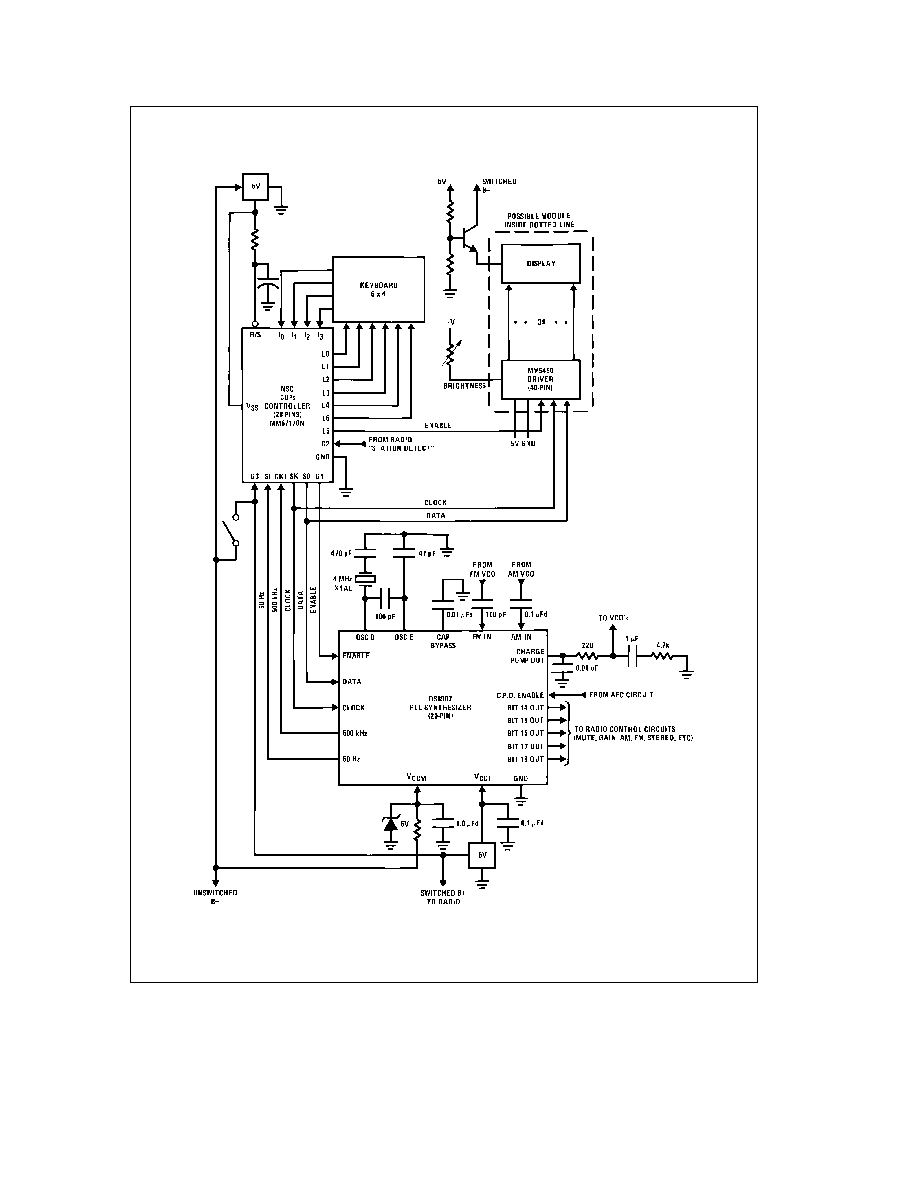
Typical Application
Electronically Tuned Radio Controller System Direct Drive LED
TL F 7511 ≠ 12
5