TL F 5111
DS8908B
AMFM
Digital
Phase-Locked
Loop
Frequency
Synthesizer
June 1990
DS8908B AM FM Digital Phase-Locked
Loop Frequency Synthesizer
General Description
The DS8908B is a PLL synthesizer designed specifically for
use in AM FM radios It contains the reference oscillator a
phase comparator a charge pump an operational amplifier
a 120 MHz ECL I
2
L dual modulus programmable divider
and a 19-bit shift register latch for serial data entry The
device is designed to operate with a serial data controller
generating the necesary division codes for each frequency
and logic state information for radio function inputs outputs
A 3 96 MHz pierce oscillator and divider chain generate a
1 98 MHz external controller clock a 20 kHz 10 kHz 9 kHz
and a 1 kHz reference signals and a 50 Hz time-of-day
signal The oscillator and divider chain are sourced by the
V
CCM
pin thus providing a low power controller clock drive
and time-of-day indication when the balance of the PLL is
powered down
The 21-bit serial data steram is transferred between the fre-
quency synthesizer and the controller via a 3-wire bus sys-
tem comprised of a data line a clock line and an enable
line
The first 2 bits in the serial data stream address the synthe-
sizer thus permitting other devices such as display drivers to
share the same bus The next 14 bits are used for the
PLL(N
a
1) divide code The 15th bit is used internally to
select the AM or FM local oscillator input A high level on
this bit enables the FM input and a low level enables the AM
input The 16th and 17th bits are used to select one of the 4
reference frequencies The 18th and 19th bits are connect-
ed via latches to open collector outputs These outputs can
be used to drive radio functions such as gain mute AM
FM or charge pump current source levels
The PLL consists of a 14-bit programmable I
2
L divider an
ECL phase comparator an ECL dual modulus (p p
a
1) pre-
scaler a high speed charge pump and an operational am-
plifier The programmable divider divides by (N
a
1) N being
the number loaded into the shift register The programmable
divider is clocked through a
d
prescaler by the AM input
or through a
d
prescaler by the FM input The AM input
will work at frequencies up to 15 MHz while the FM input
works up to 120 MHz The VCO can be tuned with a fre-
quency resolution of either 1 kHz 9 kHz 10 kHz or 20 kHz
The buffered AM and FM inputs are self-biased and can be
driven directly by the VCO through a capacitor The ECL
phase comparator produces very accurate resolution of the
phase difference between the input signal and the reference
oscillator The high speed charge pump consists of a
switchable constant current source and sink The charge
pump can be programmed to deliver from 75 mA to 750 mA
of constant current by connection of an external resistor
from pin R
PROGRAM
to ground or the open collector bit out-
puts Connection of programming resistors to the bit outputs
enables the controller to adjust the loop gain for the particu-
lar reference frequency selected The charge pump will
source current if the VCO frequency is high and sink
current if the VCO frequency is low The low noise opera-
tional amplifier provided has a high impedance JFET input
and a large output voltage range The op amp's negative
input is common with the charge pump output and its posi-
tive input is internally biased
Features
Y
Uses inexpensive 3 96 MHz reference crystal
Y
F
IN
capability greater than 120 MHz allows direct syn-
thesis at FM frequencies
Y
FM resolution of either 10 kHz or 20 kHz allows usage
of 10 7 MHz ceramic filter distribution
Y
Serial data entry for simplified control
Y
50 Hz output for time-of-day reference driven from sep-
arate low power V
CCM
Y
2 open collector buffered outputs for controlling various
radio functions or loop gain
Y
Separate AM and FM inputs AM input has 15 mV (typi-
cal) hysteresis
Y
Programmable charge pump current sources enable ad-
justment of system loop gain
Y
Operational amplifier provides high impedance load to
charge pump output and a wide voltage range for the
VCO input
Connection Diagram
Dual-In-Line Package
TL F 5111 ≠ 1
Top View
Order Number DS8908BN
See NS Package Number N20A
TRI-STATE
is a registered trademark of National Semiconductor Corp
C1995 National Semiconductor Corporation
RRD-B30M105 Printed in U S A
Absolute Maximum Ratings
(Note 1)
If Military Aerospace specified devices are required
please contact the National Semiconductor Sales
Office Distributors for availability and specifications
Supply Voltage
(V
CC1
) (V
CCM
)
7V
(V
CC2
)
17V
Input Voltage
7V
Output Voltage
7V
Storage Temperature Range
b
65 C to
a
150 C
Lead Temperature (Soldering 4 seconds)
260 C
Operating Conditions
Min
Max
Units
V
CC1
4 5
5 5
V
V
CC2
V
CC1
a
1 5
15 0
V
V
CCM
3 5
5 5
V
Temperature T
A
b
40
a
85
C
DC Electrical Characteristics
(Notes 2 and 3)
Symbol
Parameter
Conditions
Min
Typ
Max
Units
V
IH
Logical ``1'' Input Voltage
2 0
V
I
IH
Logical ``1'' Input Current
V
IN
e
2 7V
0
10
m
A
V
IL
Logical ``0'' Input Voltage
0 8
V
I
IL
Logical ``0'' Input Current
Data Clock and ENABLE Inputs V
IN
e
0V
b
5
b
25
m
A
I
OH
Logical ``1'' Output Current
V
OH
e
5 5V
50
m
A
All Bit Outputs 50 Hz Output
1 98 MHz Output
V
OH
e
2 4V V
CCM
e
4 5V
b
250
m
A
V
OL
Logical ``0'' Output Voltage
I
OL
e
5 mA
0 5
V
All Bit Outputs
50 Hz Output 1 98 MHz Output
I
OL
e
250 mA
0 5
V
1 98 MHz Output
I
OL
e
20 mA T
A
l
70 C
0 3
V
I
OL
e
20 mA T
A
s
70 C
0 4
V
I
CC1
Supply Current (V
CC1
)
All Bit Outputs High
160
mA
I
CCM
V
CCM
Supply Current
V
CCM
e
5 5V All Other Pins Open
2 5
4 0
mA
I
OUT
Charge Pump Ougtput Current
3 33k
s
R
PROG
s
33 3k
Pump Up
b
20
I
PROG
a
20
%
I
OUT
Measured between
Pump Down
b
20
I
PROG
a
20
%
Pin 17 and Pin 18
TRI-STATE
0
11
nA
I
PROG
e
V
CC1
2 R
PROG
I
CC2
V
CC2
Supply Current
V
CCM
e
5V V
CC1
e
5 5V V
CC2
e
15V
6 7
11
mA
All Other Pins Open
OP
VOH
Op Amp Minimum High Level
V
CC1
e
4 5V I
OH
e b
750 mA
V
CC2
b
0 4
V
OP
VOL
Op Amp Maximum Low Level
V
CC1
e
5 5V I
OL
e
750 mA
0 6
V
CPO
BIAS
Charge Pump Bias Voltage
CPO Shorted to Op Amp Output
Delta
CPO
e
TRI-STATE
100
mV
Op Amp I
OL
750 mA vs
b
750 mA
AC Electrical Characteristics
V
CC
e
5V T
A
e
25 C t
r
s
10 ns t
f
s
10 ns
Symbol
Parameter
Conditions
Min
Typ
Max
Units
V
IN(MIN)(F)
F
IN
Minimum Signal Input
AM and FM Inputs
b
40 C
s
T
A
s
85 C
20
100
mV(rms)
V
IN(MAX)(F)
F
IN
Maximum Signal Input
AM and FM Inputs
b
40 C
s
T
A
s
85 C
1000
1500
mV(rms)
F
OPERATE
Operating Frequency Range
V
IN
e
100 mV rms
AM
0 5
15
MHz
(Sine Wave Input)
b
40 C
s
T
A
s
85 C
FM
80
120
MHz
R
IN
(FM)
AC Input Resistance FM
120 MHz V
IN
e
100 mV rms
600
X
R
IN
(AM)
AC Input Resistance AM
15 MHz V
IN
e
100 mV rms
1000
X
C
IN
Input Capacitance FM and AM
V
IN
e
120 MHz (FM) 15 MHz (AM)
3
6
10
pF
t
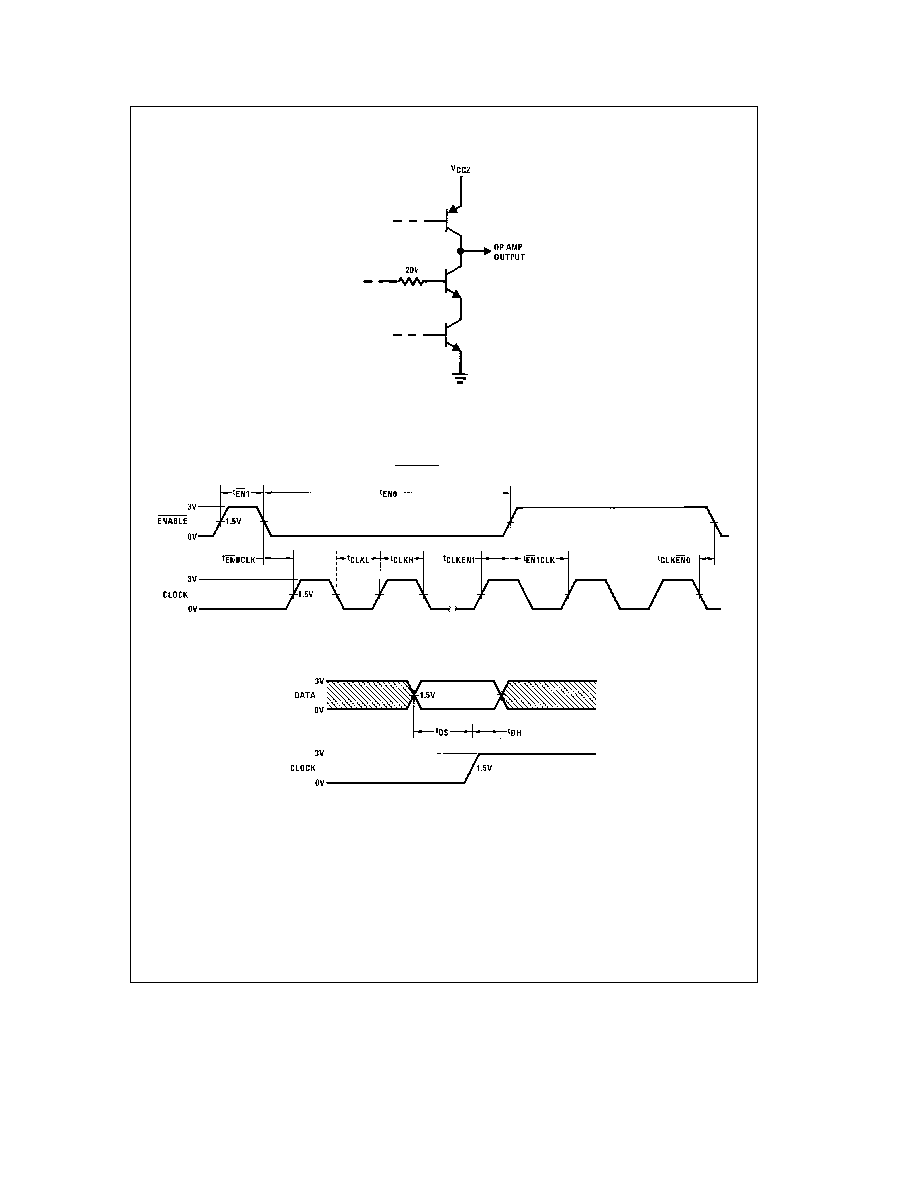
EN1
Minimum ENABLE High
625
1250
ns
Pulse Width
2
AC Electrical Characteristics
V
CC
e
5V T
A
e
25 C t
r
s
10 ns t
f
s
10 ns (Continued)
Symbol
Parameter
Conditions
Min
Typ
Max
Units
t
EN0
Minimum ENABLE Low
375
750
ns
Pulse Width
t
CLKEN0
Minimum Time before ENABLE
Goes Low That CLOCK Must
b
50
0
ns
Be Low
t
EN0CLK
Minimum Time after ENABLE
Goes Low That CLOCK Must
275
550
ns
Remain Low
t
CLKEN1
Minimum Time before ENABLE
Goes High That Last Positive
300
600
ns
CLOCK Edge May Occur
t
EN1CLK
Minimum Time after ENABLE
Goes High before an Unused
175
350
ns
Positive CLOCK Edge May Occur
t
CLKH
Minimum CLOCK High
275
550
ns
Pulse Width
t
CLKL
Minimum CLOCK Low
400
800
ns
Pulse Width
t
DS
Minimum DATA Set-Up Time
Minimum Time before CLOCK
150
300
ns
That DATA Must Be Valid
t
DH
Minimum DATA Hold Time
Minimum Time after CLOCK
400
800
ns
That DATA Must Remain Valid
Note 1
``Absolute Maximum Ratings'' are those values beyond which the safety of the device cannot be guaranteed Except for ``Operating Temperature Range''
they are not meant to imply that the devices should be operated at these limits The table of ``Electrical Characteristics'' provides conditions for actual device
operation
Note 2
Unless otherwise specified min max limits apply across the
b
40 C to
a
85 C temperature range for the DS8908B
Note 3
All currents into device pins shown as positive out of device pins as negative all voltage referenced to ground unless otherwise noted All values shown as
max or min on absolute value basis
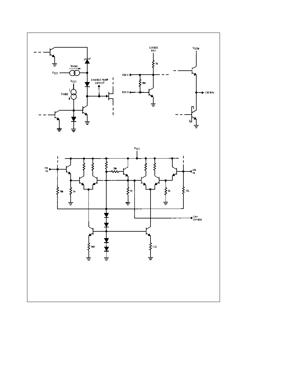
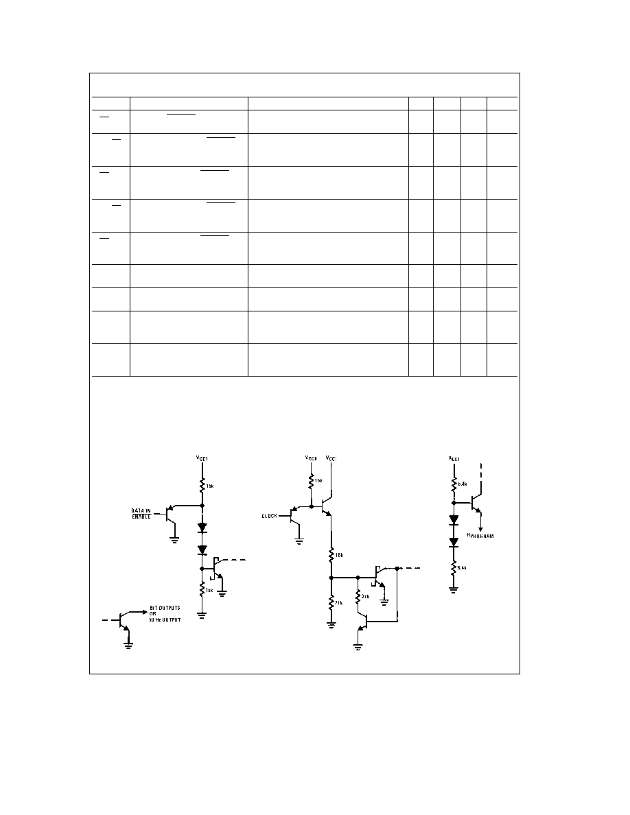
Schematic Diagrams
(DS8908B AM FM PLL Typical Input Output Schematics)
TL F 5111 ≠ 4
TL F 5111 ≠ 2
TL F 5111 ≠ 3
3