 | –≠–ª–µ–∫—Ç—Ä–æ–Ω–Ω—ã–π –∫–æ–º–ø–æ–Ω–µ–Ω—Ç: DS8925M | –°–∫–∞—á–∞—Ç—å:  PDF PDF  ZIP ZIP |
DS8925
LocalTalk
TM
Dual Driver/Triple Receiver
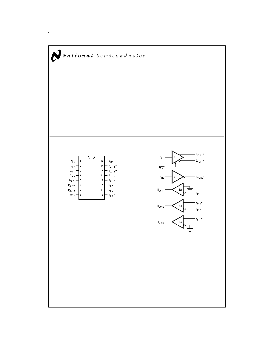
General Description
The DS8925 is a dual driver/triple receiver device optimized
to provide a single chip solution for a LocalTalk Interface.
The device provides one differential TIA/EIA-422 driver, one
TIA/EIA-423 single ended driver, one TIA/EIA-422 receiver
and two TIA/EIA-423 receivers, all in a surface mount 16 pin
package. This device is electrically similar to the 26LS30 and
26LS32 devices.
The drivers feature
±
10V common mode range, and the dif-
ferential driver provides TRI-STATEable outputs. The receiv-
ers offer
±
200 mV thresholds over the
±
10V common mode
range.
Features
n
Single chip solution for LocalTalk port
n
Two driver/three receivers per package
n
Wide common mode range:
±
10V
n
±
200 mV receiver sensitivity
n
70 mV typical receiver input hysteresis
n
Available in SOIC packaging
Connection Diagram
Functional Diagram
TRI-STATE
Æ
is a registered trademark of National Semiconductor Corporation.
LocalTalk
TM
is a trademark of Apple Computer Incorporated.
Dual-In-Line Package
DS011895-1
Order Number DS8925M
See NS Package Number M16A
DS011895-2
December 1998
DS8925
LocalT
alk
Dual
Driver/T
riple
Receiver
© 1998 National Semiconductor Corporation
DS011895
www.national.com
Absolute Maximum Ratings
(Note 1)
If Military/Aerospace specified devices are required,
please contact the National Semiconductor Sales Office/
Distributors for availability and specifications.
Supply Voltage (V
CC
)
+7V
Supply Voltage (V
EE
)
-7V
Enable Input Voltage (D
EN1
)
+7V
Driver Input Voltage (D
IN
)
+7V
Driver Output Voltage (Power Off: D
OUT
)
±
15V
Receiver Input Voltage
(V
ID
: R
IN
+ - R
IN
-)
±
25V
Receiver Input Voltage
(V
CM
: (R
IN
+ + R
IN
-)/2)
±
25V
Receiver Input Voltage
(Input to GND: R
IN
)
±
25V
Receiver Output Voltage (R
OUT
)
+5.5V
Maximum Package Power Dissipation
@
+25∞C M Package
1.33W
Derate M Package 10.6 mW/∞C above
+25∞C
Storage Temperature Range
-65∞C to +150∞C
Lead Temperature Range
(Soldering, 4 Sec.)
+260∞C
This Device Does Not Meet 2000V
ESD Rating
(Note 7)
Recommended Operating
Conditions
Min
Typ
Max
Units
Supply Voltage (V
CC
)
+4.75
+5.0
+5.25
V
Supply Voltage (V
EE
)
-4.75
-5.0
-5.25
V
Operating Free Air
Temperature (T
A
)
0
25
70
∞C
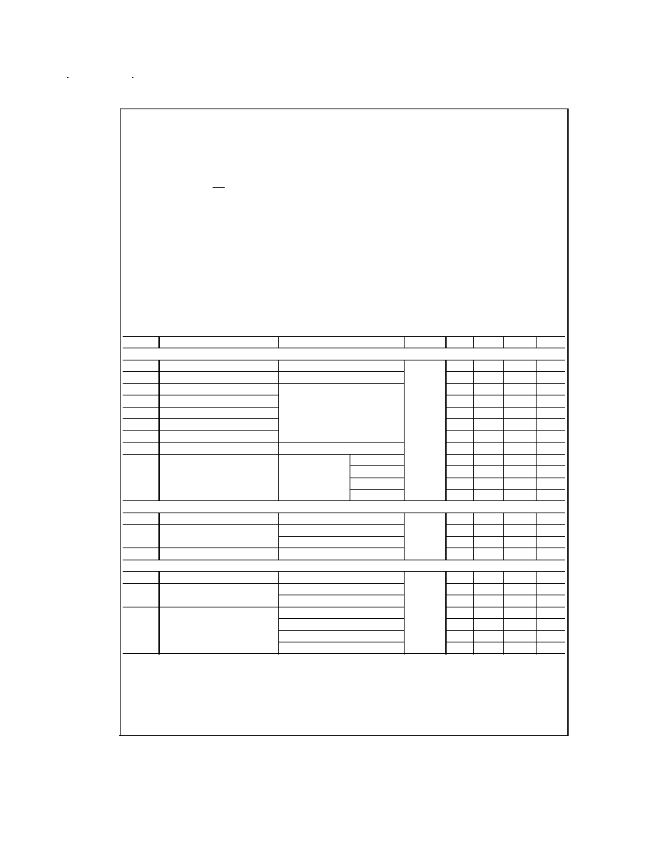
Electrical Characteristics
(Notes 2, 3)
Over Supply Voltage and Operating Temperature ranges, unless otherwise specified
Symbol
Parameter
Conditions
Pin
Min
Typ
Max
Units
DIFFERENTIAL DRIVER CHARACTERISTICS
V
OD
Output Differential Voltage
R
L
=
or R
L
= 3.9 k
D
OUT
+,
D
OUT
-
±
7
±
9.0
±
10
V
V
O
Output Voltage
R
L
=
or R
L
= 3.9 k
±
4.5
±
5.25
V
V
OD1
Output Differential Voltage
R
L
= 100
,
Figure 1
4.0
6.4
|V|
V
SS
|V
OD1
- V
OD1
*
|
8.0
12.8
|V|
V
OD1
Output Unbalance
0.02
0.4
V
V
OS
Offset Voltage
0
3
V
V
OS
Offset Unbalance
0.05
0.4
V
V
OD2
Output Differential Voltage
RL = 140
,
Figure 1
6.0
7.0
|V|
I
OZD
TRI-STATE
Æ
Leakage Current
V
CC
= 5.25V
V
O
= +10V
2
150
µA
V
EE
= -5.25V
V
O
= +6V
1
100
µA
V
O
= -6V
-1
-100
µA
V
O
= -10V
-2
-150
µA
SINGLE ENDED DRIVER CHARACTERISTICS
V
O
Output Voltage (No Load)
R
L
=
or R
L
= 3.9 k
,
Figure 2
D
OUT
-
4
4.4
6
|V|
V
T
Output Voltage
R
L
= 3 k
,
Figure 2
3.7
4.3
|V|
R
L
= 450
,
Figure 2
3.6
4.1
|V|
V
T
Output Unbalance
0.02
0.4
V
DRIVER CHARACTERISTICS
V
CM
Common Mode Range
Power Off, or D1 Disabled
D
OUT
+,
D
OUT
-
±
10
V
I
OSD
Short Circuit Current
V
O
= 0V, Sourcing Current
-80
-150
mA
V
O
= 0V, Sinking Current
80
150
mA
I
OXD
Power-Off Leakage Current
(V
CC
= V
EE
= 0V)
V
O
= +10V
2
150
µA
V
O
= +6V
1
100
µA
V
O
= -6V
-1
-100
µA
V
O
= -10V
-2
-150
µA
www.national.com
2
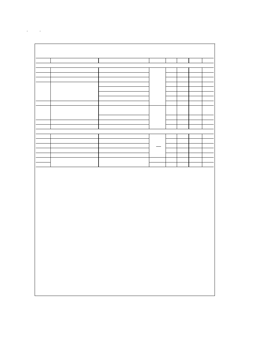
Electrical Characteristics
(Notes 2, 3) (Continued)
Over Supply Voltage and Operating Temperature ranges, unless otherwise specified
Symbol
Parameter
Conditions
Pin
Min
Typ
Max
Units
RECEIVER CHARACTERISTICS
V
TH
Input Threshold
-7V
V
CM
+7V
R
IN
+,
R
IN
-
-200
±
35
+200
mV
V
HY
Hysteresis
V
CM
= 0V
70
mV
R
IN
Input Resistance
-10V
V
CM
+10V
6.0
8.5
k
I
IN
Input Current (Other Input = 0V,
Power On, or V
CC
= V
EE
= 0V)
V
IN
= +10V
3.25
mA
V
IN
= +3V
0
1.50
mA
V
IN
= -3V
0
-1.50
mA
V
IN
= -10V
-3.25
mA
V
IB
Input Balance Test
R
S
= 500
(R2 only)
±
400
mV
V
OH
High Level Output Voltage
I
OH
= -400 µA,
R
OUT
2.7
4.2
V
V
IN
= +200 mV
I
OH
= -400 µA, V
IN
= OPEN
2.7
4.2
V
V
OL
Low Level Output Voltage
I
OL
= 8.0 mA, V
IN
= -200 mV
0.3
0.5
V
I
OSR
Short Circuit Current
V
O
= 0V
-15
-34
-85
mA
DEVICE CHARACTERISTICS
V
IH
High Level Input Voltage
D
IN
,
D
EN1
2.0
V
V
IL
Low Level Input Voltage
0.8
V
I
IH
High Level Input Current
V
IN
= 2.4V
1
40
µA
I
IL
Low Level Input Current
V
IN
= 0.4V
-10
-200
µA
V
CL
Input Clamp Voltage
I
IN
= -12 mA
-1.5
V
I
CC
Power Supply Current
No Load
V
CC
40
65
mA
I
EE
D1 Enabled or Disabled
V
EE
-5
-15
mA
www.national.com
3
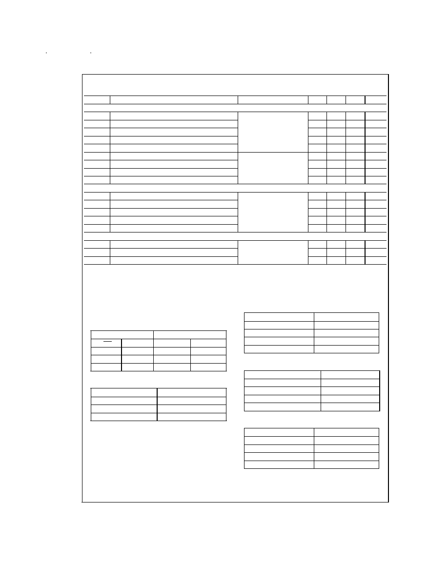
Switching Characteristics
(Notes 4, 5)
Over Supply Voltage and Operating Temperature Ranges, unless otherwise specified
Symbol
Parameter
Conditions
Min
Typ
Max
Units
DIFFERENTIAL DRIVER CHARACTERISTICS
t
PHLD
Differential Propagation Delay High to Low
R
L
= 100
, C
L
= 500 pF,
(
Figures 3, 4)
C
1
= C
2
= 50 pF
70
134
350
ns
t
PLHD
Differential Propagation Delay Low to High
70
141
350
ns
t
SKD
Differential Skew |t
PHLD
- t
PLHD
|
7
50
ns
t
r
Rise Time
50
140
300
ns
t
f
Fall Time
50
140
300
ns
t
PHZ
Disable Time High to Z
R
L
= 100
, C
L
= 500 pF
(
Figures 7, 8)
300
600
ns
t
PLZ
Disable Time Low to Z
300
600
ns
t
PZH
Enable Time Z to High
160
350
ns
t
PZL
Enable Time Z to Low
160
350
ns
SINGLE ENDED DRIVER CHARACTERISTICS
t
PHL
Propagation Delay High to Low
R
L
= 450
, C
L
= 500 pF
(
Figures 5, 6)
70
120
350
ns
t
PLH
Propagation Delay Low to High
70
150
350
ns
t
SK
Skew, |t
PHL
- t
PLH
30
70
ns
t
r
Rise Time
50
100
300
ns
t
f
Fall Time
20
50
300
ns
RECEIVER CHARACTERISTICS
t
PHL
Propagation Delay High to Low
C
L
= 15 pF
(
Figures 9, 10)
10
33
75
ns
t
PLH
Propagation Delay Low to High
10
30
75
ns
t
SK
Skew, |t
PHL
- t
PLH
|
3
20
ns
Note 1: Absolute Maximum Ratings are those values beyond which the safety of the device cannot be guaranteed. They are not meant to imply that the devices
should be operated at these limits. The table of Electrical Characteristics specifies conditions of device operation.
Note 2: Current into device pins is defined as positive. Current out of device pins is defined as negative. All voltages are referenced to ground except V
OD
, V
OD1
,
V
OD2
, and V
SS
.
Note 3: All typicals are given for: V
CC
= +5.0V, V
EE
= -5.0V, T
A
= +25∞C unless otherwise specified.
Truth Tables
Driver (D1)
Inputs
Outputs
D
EN1
D
IN1
D
OUT1
+
D
OUT1
-
H
X
Z
Z
L
L
L
H
L
H
H
L
Driver (D2)
Input
Output
D
IN2
D
OUT2
-
L
H
H
L
H = Logic High Level (Steady State)
L = Logic Low Level (Steady State)
X = Irrelevant (Any Input)
Z = Off State (TRI-STATE, High Impedance)
OPEN = Non-Terminated
Receiver (1)
Input
Output
R
IN1
-
R
OUT1
-200 mV
H
+200 mV
L
OPEN
H
Receiver (2)
Inputs
Output
R
IN2
+ - R
IN2
-
R
OUT2
-200 mV
L
+200 mV
H
OPEN
H
Receiver (3)
Input
Output
R
IN3
+
R
OUT3
-200 mV
L
+200 mV
H
OPEN
H
www.national.com
4
Parameter Measurement Information
DS011895-3
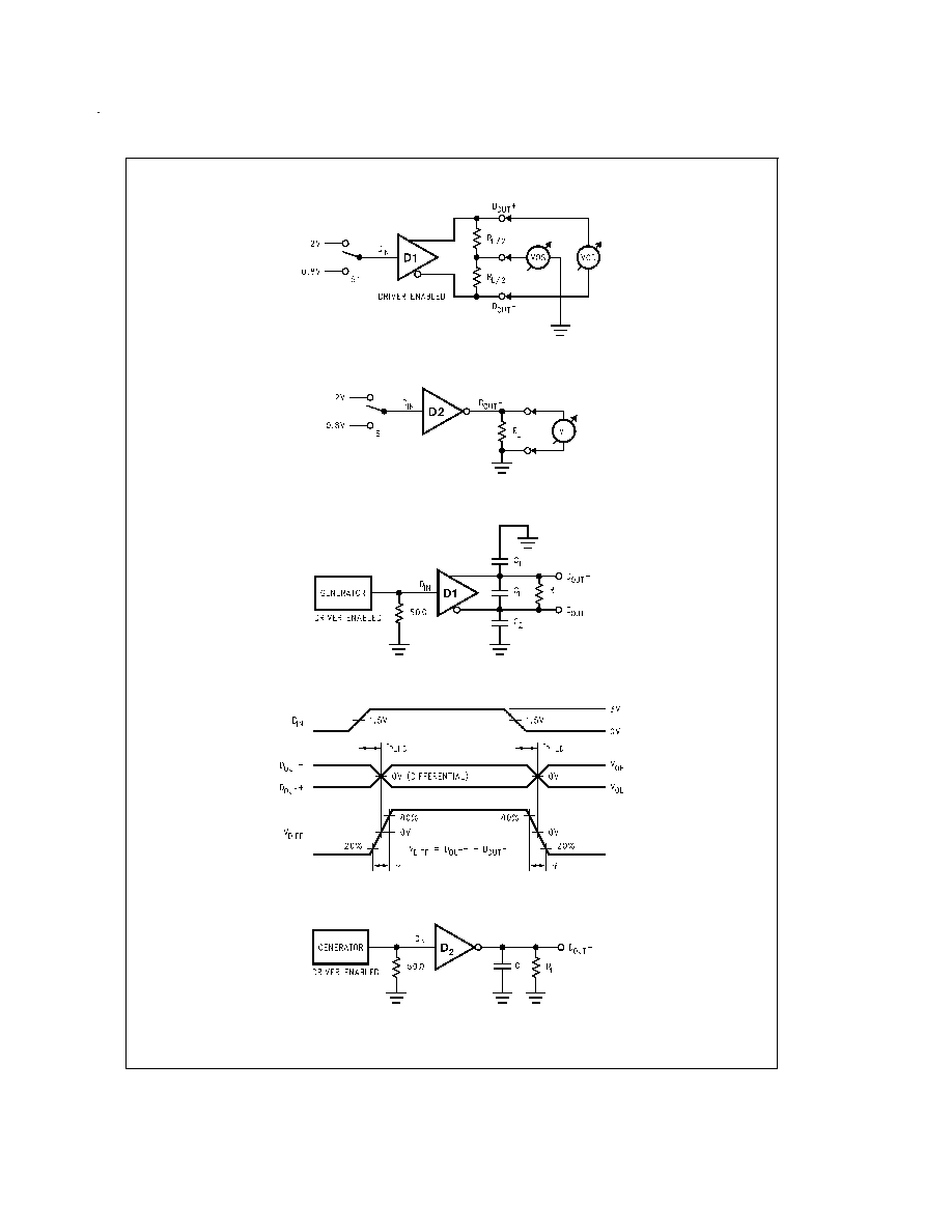
FIGURE 1. Differential Driver DC Test Circuit
DS011895-4
FIGURE 2. Single Ended Driver DC Test Circuit
DS011895-5
FIGURE 3. Differential Driver Propagation Delay and Transition Time Test Circuit
DS011895-6
FIGURE 4. Differential Driver Propagation Delay and Transition Time Waveforms
DS011895-7
FIGURE 5. Single Ended Driver Propagation Delay and Transition Time Test Circuit
www.national.com
5