DS89C387
Twelve Channel CMOS Differential Line Driver
General Description
The DS89C387 is a high speed twelve channel CMOS differ-
ential driver that meets the requirements of TIA/EIA-422-B.
The DS89C387 features a low I
CC
specification of 1.5 mA
maximum, which makes it ideal for battery powered and
power conscious applications. The device replaces three
DS34C87s and offers a PC board space savings up to 30%.
The twelve channel driver is available in a SSOP package.
The device is ideal for wide parallel bus applications.
Each TRI-STATE
Æ
enable (EN) allows the driver outputs to
be active or in a HI-impedance off state. Each enable is com-
mon to only two drivers for flexibility and control. The drivers
may be disabled to turn off load current and to save power
when data is not being transmitted.
The driver's input (DI) is compatible with both TTL and
CMOS signal levels.
Features
n
Low power I
CC
: 1.5 mA maximum
n
Meets TIA/EIA-422-B (RS-422)
n
Guaranteed AC parameters:
-- Maximum driver skew
-3 ns
-- Maximum transition time
-10 ns
n
Available in SSOP packaging:
-- Requires 30% less PCB space than 3 DS34C87TMs
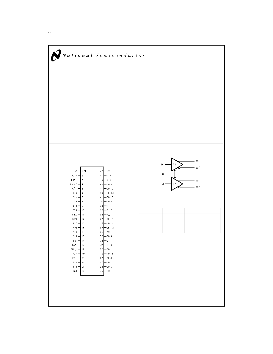
Connection Diagram
Functional Diagram
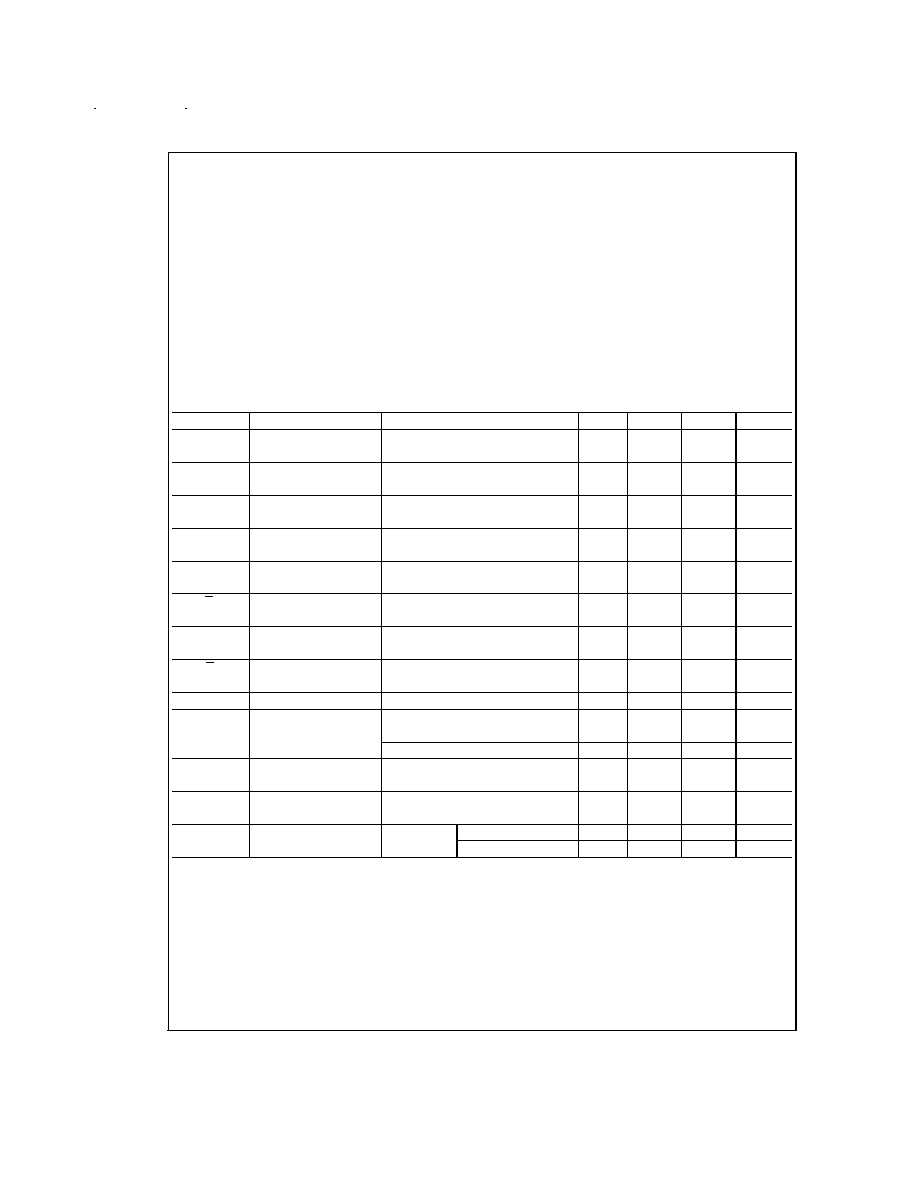
Truth Table
Enable
Input
Outputs
EN
DI
DO
DO
*
L
X
Z
Z
H
H
H
L
H
L
L
H
TRI-STATE
Æ
is a registered trademark of National Semiconductor Corporation.
48L SSOP
DS89C387
DS012086-1
Order Number DS89C387TMEA
See NS Package Number MS48A
DS012086-2
1/6 of package
May 1995
DS89C387
T
welve
Channel
CMOS
Differential
Line
Driver
© 1998 National Semiconductor Corporation
DS012086
www.national.com
Absolute Maximum Ratings
(Notes 1, 2)
If Military/Aerospace specified devices are required,
please contact the National Semiconductor Sales Office/
Distributors for availability and specifications.
Supply Voltage (V
CC
)
-0.5 to 7.0V
DC Voltage (V
IN
)
-1.5 to V
CC
+1.5V
DC Output Voltage (V
OUT
)
-0.5 to 7V
Clamp Diode Current (I
IK
, I
OK
)
±
20 mA
DC Output Current, per pin (I
OUT
)
±
150 mA
DC V
CC
or GND Current (I
CC
)
±
500 mA
Storage Temperature Range (T
STG
)
-65∞C to +150∞C
Maximum Power Dissipation (P
D
)
@
25∞C (Note 3)
SSOP Package
1359 mW
Lead Temperature (T
L
)
(Soldering 4 sec.)
260∞C
This device does not meet 2000V ESD rating. (Note 11)
Operating Conditions
Min
Max
Units
Supply Voltage (V
CC
)
4.50
5.50
V
DC Input or Output Voltage (V
IN
, V
OUT
)
0
V
CC
V
Operating Temperature Range (T
A
)
DS89C387T
-40
+85
∞C
Input Rise or Fall Times (t
r
, t
f
)
500
ns
DC Electrical Characteristics
(Notes 2, 4)
V
CC
= 5V
±
10% (unless otherwise specified)
Symbol
Parameter
Conditions
Min
Typ
Max
Units
V
IH
High Level Input
2.0
V
CC
V
Voltage
V
IL
Low Level Input
GND
0.8
V
Voltage
V
OH
High Level Output
V
IN
= V
IH
or V
IL
,
2.5
3.4
V
Voltage
I
OUT
= -20 mA
V
OL
Low Level Output
V
IN
= V
IH
or V
IL
,
0.3
0.5
V
Voltage
I
OUT
= 48 mA
V
T
Differential Output
R
L
= 100
2.0
3.1
V
Voltage
(Note 5)
|V
T
|≠|V
T
|
Difference In
R
L
= 100
0.4
V
Differential Output
(Note 5)
V
OS
Common Mode
R
L
= 100
2.0
3.0
V
Output Voltage
(Note 5)
|V
OS
≠V
OS
|
Difference In
R
L
= 100
0.4
V
Common Mode Output
(Note 5)
I
IN
Input Current
V
IN
= V
CC
, GND, V
IH
, or V
IL
±
1.0
µA
I
CC
Quiescent Supply
I
OUT
= 0 µA,
600
1500
µA
Current
V
IN
= V
CC
or GND
V
IN
= 2.4V or 0.5V (Note 6)
0.8
2.0
mA
I
OZ
TRI-STATE Output
V
OUT
= V
CC
or GND
±
0.5
±
5.0
µA
Leakage Current
Control = V
IL
I
SC
Output Short
V
IN
= V
CC
or GND
-30
-115
-150
mA
Circuit Current
(Notes 5, 7)
I
OFF
Power Off Output
V
CC
= 0V
V
OUT
= 6V
100
µA
Leakage Current
(Note 5)
V
OUT
= -0.25V
-100
µA
Note 1: Absolute Maximum Ratings are those values beyond which the safety of the device cannot be guaranteed. They are not meant to imply that the device
should be operated at these limits. The table of "Electrical Characteristics" provide conditions for actual device operation.
Note 2: Unless otherwise specified, all voltages are referenced to ground. All currents into device pins are positive; all currents out of device pins are negative.
Note 3: Ratings apply to ambient temperature at 25∞C. Above this temperature derate SSOP (MEA) Package 10.9 mW/∞C.
Note 4: Unless otherwise specified, min/max limits apply across the -40∞C to 85∞C temperature range. All typicals are given for V
CC
= 5V and T
A
= 25∞C.
Note 5: See TIA/EIA-422-B for exact test conditions.
Note 6: Measured per input. All other inputs at V
CC
or GND.
Note 7: This is the current sourced when a high output is shorted to ground. Only one output at a time should be shorted.
www.national.com
2
Switching Characteristics
(Note 4)
V
CC
= 5V
±
10%, t
r
, t
f
6 ns (
Figures 1, 2, 3, 4)
Symbol
Parameter
Conditions
Min
Typ
Max
Units
t
PLH
, t
PHL
Propagation Delay
S1 Open
2
6
11
ns
Input to Output
Skew
(Note 8)
S1 Open
0
0.5
3
ns
t
TLH
, t
THL
Differential Output Rise
S1 Open
6
10
ns
And Fall Times
t
PZH
Output Enable Time
S1 Closed
12
25
ns
t
PZL
Output Enable Time
S1 Closed
13
26
ns
t
PHZ
Output Disable Time (Note 9)
S1 Closed
4
8
ns
t
PLZ
Output Disable Time (Note 9)
S1 Closed
6
12
ns
C
PD
Power Dissipation
100
pF
Capacitance (Note 10)
C
IN
Input Capacitance
6
pF
Note 8: Skew is defined as the difference in propagation delays between complementary outputs at the crossing point.
Note 9: Output disable time is the delay from the control input being switched to the output transistors turning off. The actual disable times are less than indicated
due to the delay added by the RC time constant of the load.
Note 10: C
PD
determines the no load dynamic power consumption, P
D
= C
PD
V
2
CC f + I
CC
V
CC
, and the no load dynamic current consumption, I
S
= C
PD
V
CC
f +
I
CC
.
Note 11: ESD Rating: HBM (1.5 k
, 100 pF)
Inputs
1500V
Outputs
1000V
EIAJ (0
, 200 pF)
All Pins
350V
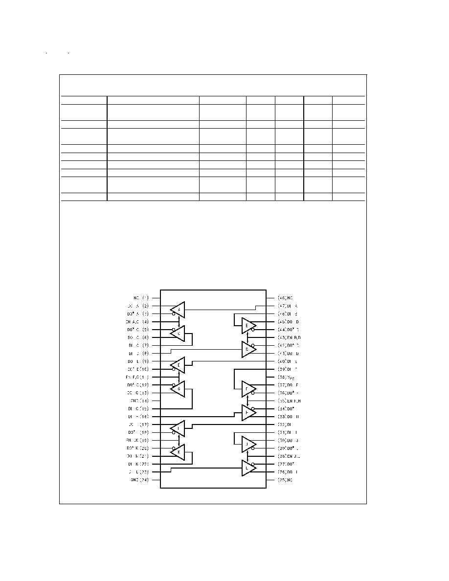
Logic Diagram
DS012086-3
www.national.com
3
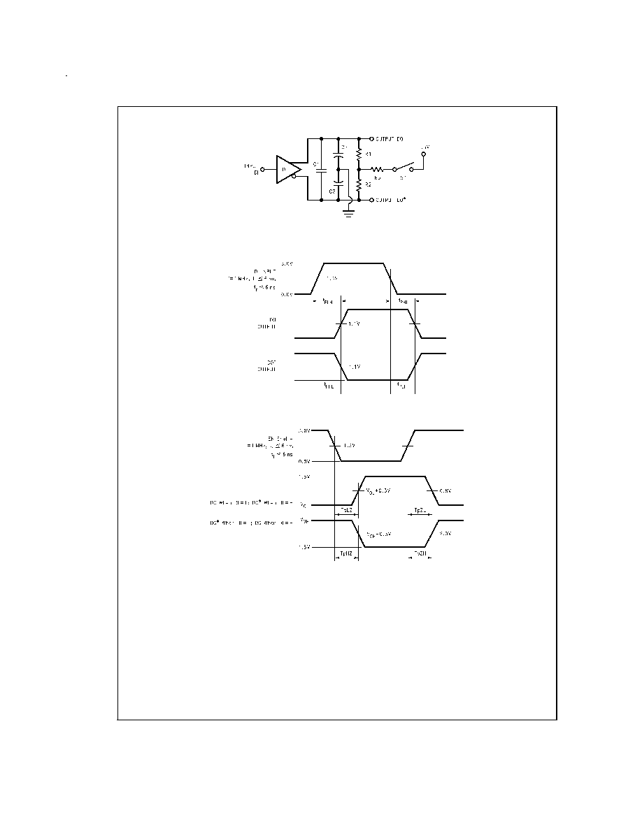
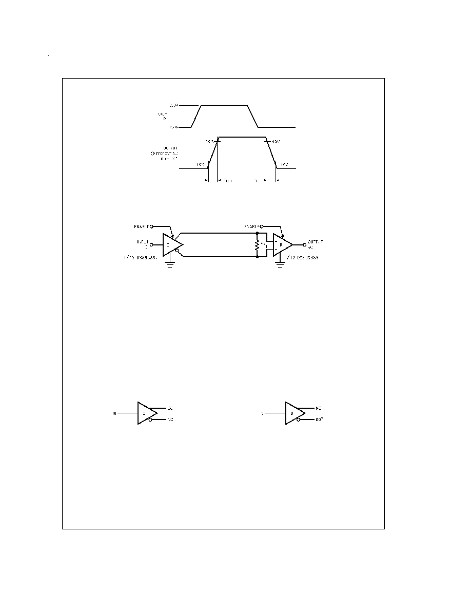
Parameter Measurement Information
DS012086-4
C1 = C2 = C3 = 40 pF (including Probe and Jig Capacitance), R1 = R2 = 50
, R3 = 500
FIGURE 1. AC Test Circuit
DS012086-5
FIGURE 2. Propagation Delays
DS012086-6
FIGURE 3. Enable and Disable Times
www.national.com
4
Parameter Measurement Information
(Continued)
Typical Application
Application Information
SKEW
Skew may be thought of in a lot of different ways, the next
few paragraphs should clarify what is represented by "Skew"
in the datasheet and how it is determined. Skew, as used in
this databook, is the absolute value of a mathematical differ-
ence between two propagation delays. This is commonly ac-
cepted throughout the semiconductor industry. However,
there is no standardized method of measuring propagation
delay, from which skew is calculated, of differential line driv-
ers. Elucidating, the voltage level, at which propagation de-
lays are measured, on both input and output waveforms are
not always consistant. Therefore, skew calculated in this
datasheet, may not be calculated the same as skew defined
in another. This is important to remember whenever making
a skew comparison.
Skew may be calculated for the DS89C387, from many dif-
ferent propagation delay measurements. They may be clas-
sified into three categories, single-ended, differential, and
complementry. Single-ended skew is calculated from t
PHL
and t
PLH
measurements (see
Figures 6, 7). Differential skew
is calculated from t
PHLD
and t
PLHD
measurements (see
Fig-
ures 8, 9). Complementry skew is calculated from t
PHL
and
t
PLH
measurements (see
Figures 10, 11).
DS012086-7
Input pulse; f = 1 MHz, 50%, t
r
6 ns, t
f
6 ns
FIGURE 4. Differential Rise and Fall Times
DS012086-8
* R
T
is optional although highly recommended to reduce reflection.
FIGURE 5. Two-Wire Balanced System, RS-422
(Circuit 1)
DS012086-9
(Circuit 2)
DS012086-10
FIGURE 6. Circuits for Measuring Single-Ended Propagation Delays (See
Figure 7)
www.national.com
5