DS90C241/DS90C124
5-35MHz DC-Balanced 24-Bit LVDS Serializer and
Deserializer
General Description
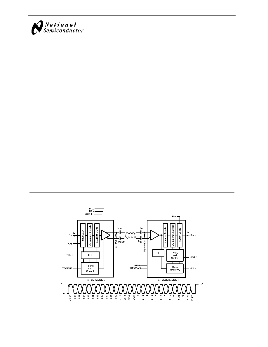
The DS90C241/124 Chipset translates a 24-bit parallel bus
into a fully transparent data/control LVDS serial stream with
embedded clock information. This single serial stream sim-
plifies transferring a 24-bit bus over PCB traces and cable by
eliminating the skew problems between parallel data and
clock paths. It saves system cost by narrowing data paths
that in turn reduce PCB layers, cable width, and connector
size and pins.
The DS90C241/124 incorporates LVDS signaling on the
high-speed I/O. LVDS provides a low power and low noise
environment for reliably transferring data over a serial trans-
mission path. By optimizing the serializer output edge rate
for the operating frequency range EMI is further reduced.
In addition the device features pre-emphasis to boost signals
over longer distances using lossy cables. Internal DC bal-
anced encoding/decoding is used to support AC-Coupled
interconnects.
Features
n
5 MHz≠35 MHz clock embedded and DC-Balancing
24:1 and 1:24 data transmissions
n
User defined Pre-Emphasis driving ability through
external resistor on LVDS outputs and capable to drive
up to 10 meters shielded twisted-pair cable
n
User selectable clock edge for parallel data on both
Transmitter and Receiver
n
Internal DC Balancing encode/decode ≠ Supports
AC-coupling interface with no external coding required
n
Individual power-down controls for both Transmitter and
Receiver
n
Embedded clock CDR (clock and data recovery) on
Receiver and no external source of reference clock
needed
n
All codes RDL (random data lock) to support
hot-pluggable applications
n
LOCK output flag to ensure data integrity at Receiver
side
n
Balanced T
SETUP
/T
HOLD
between RCLK and RDATA on
Receiver side
n
PTO (progressive turn-on) LVCMOS outputs to reduce
EMI and minimize SSO effects
n
All LVCMOS inputs and control pins have internal
pulldown
n
On-chip filters for PLLs on Transmitter and Receiver
n
48-pin TQFP package
n
Pure CMOS .35 µm process
n
Power supply range 3.3V
±
10%
n
Temperature range ≠40∞C to +105∞C
n
8 kV HBM ESD structure
Block Diagram
20171901
TRI-STATE
Æ
is a registered trademark of National Semiconductor Corporation.
PRELIMINARY
July 2006
DS90C241/DS90C124
5-35MHz
DC-Balanced
24-Bit
L
VDS
Serializer
and
Deserializer
© 2006 National Semiconductor Corporation
DS201719
www.national.com

Absolute Maximum Ratings
(Note 1)
If Military/Aerospace specified devices are required,
please contact the National Semiconductor Sales Office/
Distributors for availability and specifications.
Supply Voltage (V
CC
)
-0.3V to +4V
LVCMOS/LVTTL Input Voltage
-0.3V to (V
CC
+0.3V)
LVCMOS/LVTTL Output Voltage
-0.3V to (V
CC
+0.3V)
LVDS Receiver Input Voltage
-0.3V to 3.9V
LVDS Driver Output Voltage
-0.3V to 3.9V
LVDS Output Short Circuit Duration
10 ms
Junction Temperature
+150∞C
Storage Temperature
-65∞C to +150∞C
Lead Temperature
(Soldering, 4 seconds)
+260∞C
Maximum Package Power Dissipation Capacity Package
De-rating:
48L TQFP
1/
JA
∞C/W above +25∞C
DS90C241
JA
45.8 (4L*); 75.4 (2L*) ∞C/W
JC
21.0∞C/W
DS90C124
JA
45.4 (4L*); 75.0 (2L*)∞C/W
JC
21.1∞C/W
*JEDEC
ESD Rating (HBM)
>
8 kV
ESD Rating (ISO10605)
DS90C241 meets ISO 10605
R
D
= 2 k
, C
S
= 330 pF
Contact Discharge (D
OUT+
, D
OUT-
) to GND
±
10 kV
Air Discharge (D
OUT+
, D
OUT-
) to GND
±
30 kV
Recommended Operating
Conditions
Min
Nom
Max
Units
Supply Voltage (V
CC
)
3.0
3.3
3.6
V
Operating Free Air
Temperature (T
A
)
-40
+25
+105
∞C
Clock Rate
5
35
MHz
Supply Noise
±
100
mV
P-P
Electrical Characteristics
Over recommended operating supply and temperature ranges unless otherwise specified.
Symbol
Parameter
Conditions
Pin/Freq.
Min
Typ
Max
Units
LVCMOS/LVTTL DC SPECIFICATIONS
V
IH
High Level Voltage
Tx: DIN[23:0], TCLK,
TPWDNB, DEN, TRFB,
DCAOFF, DCBOFF,
VODSEL
Rx: RPWDNB, RRFB,
REN
2.0
V
CC
V
V
IL
Low Level Input Voltage
GND
0.8
V
V
CL
Input Clamp Voltage
I
CL
= -18 mA
(Note 8)
-0.8
-1.5
V
I
IN
Input Current
V
IN
= 0V or 3.6V
Tx: DIN[23:0], TCLK,
TPWDNB, DEN, TRFB,
DCAOFF, DCBOFF,
VODSEL
-10
±
5
+10
µA
Rx: RPWDNB, RRFB,
REN
-20
±
5
+20
µA
V
OH
High Level Output Voltage
I
OH
= -4 mA
Rx: ROUT[23:0], RCLK,
LOCK
2.3
3.0
V
CC
V
V
OL
Low Level Output Voltage
I
OL
= +4 mA
GND
0.33
0.5
V
I
OS
Output Short Circuit Current
V
OUT
= 0V
(Note 8)
-40
-70
-110
mA
I
OZ
TRI-STATE
Æ
Output Current
RPWDNB, REN = 0V
V
OUT
= 0V or 2.4V
Rx: ROUT[23:0], RCLK,
LOCK
-30
±
0.4
+30
µA
LVDS DC SPECIFICATIONS
V
TH
Differential Threshold High
Voltage
V
CM
= +1.2V
Rx: R
IN+
, R
IN-
+100
mV
V
TL
Differential Threshold Low
Voltage
-100
mV
I
IN
Input Current
V
IN
= +2.4V,
V
CC
= 3.6V or 0V
±
250
µA
V
IN
= 0V, V
CC
= 3.6V or 0V
±
250
µA
DS90C241/DS90C124
www.national.com
2

Electrical Characteristics
(Continued)
Over recommended operating supply and temperature ranges unless otherwise specified.
Symbol
Parameter
Conditions
Pin/Freq.
Min
Typ
Max
Units
LVDS DC SPECIFICATIONS
V
OD
Output Differential Voltage
(D
OUT+
)≠(D
OUT-
)
R
L
= 100
, w/o Pre-emphasis
VODSEL = L
(VODSEL = H) (Figure 16)
Tx: D
OUT+
, D
OUT-
250
(450)
400
(750)
600
(1200)
mV
V
OD
Output Differential Voltage
Unbalance
R
L
= 100
, w/o Pre-emphasis
10
50
mV
V
OS
Offset Voltage
R
L
= 100
, w/o Pre-emphasis
1.00
1.25
1.50
V
V
OS
Offset Voltage Unbalance
R
L
= 100
, w/o Pre-emphasis
1
50
mV
I
OS
Output Short Circuit Current
DOUT = 0V, DIN = H,
TPWDNB, DEN = 2.4V,
VODSEL = L
-2
-8
mA
DOUT = 0V, DIN = H,
TPWDNB, DEN = 2.4V,
VODSEL = H
-7
-13
mA
I
OZ
TRI-STATE Output Current
TPWDNB, DEN = 0V,
DOUT = 0V or 2.4V
-15
±
1
+15
µA
SER/DES SUPPLY CURRENT (DVDD*, PVDD* and AVDD* pins) *Digital, PLL, and Analog VDDs
I
CCT
Serializer (Tx)
Total Supply Current
(includes load current)
R
L
= 100
R
PRE
= OFF
VODSEL = H/L
Checker-board pattern (Figure 1)
f = 35 MHz
40
65
mA
R
L
= 100
R
PRE
= 6 k
VODSEL = H/L
Checker-board pattern (Figure 1)
f = 35 MHz
45
70
mA
Serializer (Tx)
Total Supply Current
(includes load current)
R
L
= 100
R
PRE
= OFF
VODSEL = H/L
f = 35 MHz
40
65
mA
R
L
= 100
R
PRE
= 6 k
VODSEL = H/L
Random pattern
f = 35 MHz
45
70
mA
I
CCTZ
Serializer (Tx)
Supply Current Power-down
TPWDNB = 0V
(All other LVCMOS Inputs = 0V)
800
µA
I
CCR
Deserializer (Rx)
Total Supply Current
(includes load current)
C
L
= 8 pF LVCMOS Output
Checker-board pattern
(Figure 2)
f = 35 MHz
75
mA
Deserializer (Rx)
Total Supply Current
(includes load current)
C
L
= 8 pF LVCMOS Output
Random pattern
f = 35 MHz
50
mA
I
CCRZ
Deserializer (Rx)
Supply Current Power-down
RPWDNB = 0V
(All other LVCMOS Inputs = 0V,
R
IN+
/ R
IN-
= 0V)
800
µA
Serializer Timing Requirements for TCLK
Over recommended operating supply and temperature ranges unless otherwise specified.
Symbol
Parameter
Conditions
Min
Typ
Max
Units
t
TCP
Transmit Clock Period
(Figure 6)
28.6
T
200
ns
t
TCIH
Transmit Clock High Time
0.4T
0.5T
0.6T
ns
t
TCIL
Transmit Clock Low Time
0.4T
0.5T
0.6T
ns
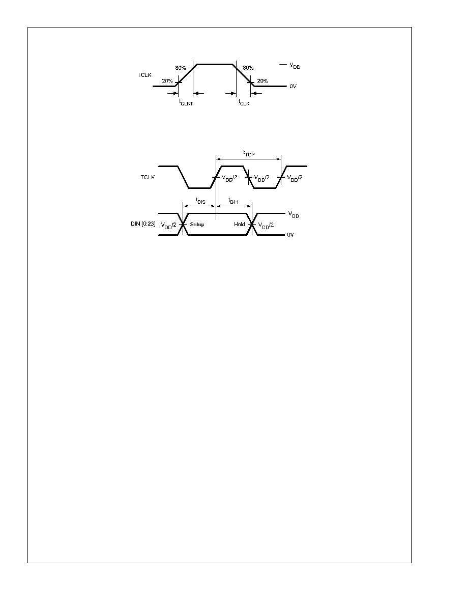
t
CLKT
TCLK Input Transition Time
(Figure 5)
3
6
ns
DS90C241/DS90C124
www.national.com
3
Serializer Timing Requirements for TCLK
(Continued)
Over recommended operating supply and temperature ranges unless otherwise specified.
Symbol
Parameter
Conditions
Min
Typ
Max
Units
t
JIT
TCLK Input Jitter
(Note 9)
33
ps
(RMS)
Serializer Switching Characteristics
Over recommended operating supply and temperature ranges unless otherwise specified.
Symbol
Parameter
Conditions
Min
Typ
Max
Units
t
LLHT
LVDS Low-to-High Transition Time
R
L
= 100
, (Figure 3)
C
L
= 10 pF to GND
VODSEL = L
0.6
ns
t
LHLT
LVDS High-to-Low Transition Time
0.6
ns
t
DIS
DIN (23:0) Setup to TCLK
R
L
= 100
,
C
L
= 10 pF to GND
(Note 8)
5
ns
t
DIH
DIN (23:0) Hold from TCLK
5
ns
t
HZD
DOUT
±
HIGH to TRI-STATE Delay
R
L
= 100
,
C
L
= 10 pF to GND
(Figure 7) (Note 4)
15
ns
t
LZD
DOUT
±
LOW to TRI-STATE Delay
15
ns
t
ZHD
DOUT
±
TRI-STATE to HIGH Delay
200
ns
t
ZLD
DOUT
±
TRI-STATE to LOW Delay
200
ns
t
PLD
Serializer PLL Lock Time
R
L
= 100
, (Figure 8)
10
ms
t
SD
Serializer Delay
R
L
= 100
, (Figure 9)
VODSEL = L, TRFB = H
3.5T + 2.85
3.5T
+ 10
ns
R
L
= 100
, (Figure 9)
VODSEL = L, TRFB = L
3.5T + 2.85
3.5T
+ 10
ns
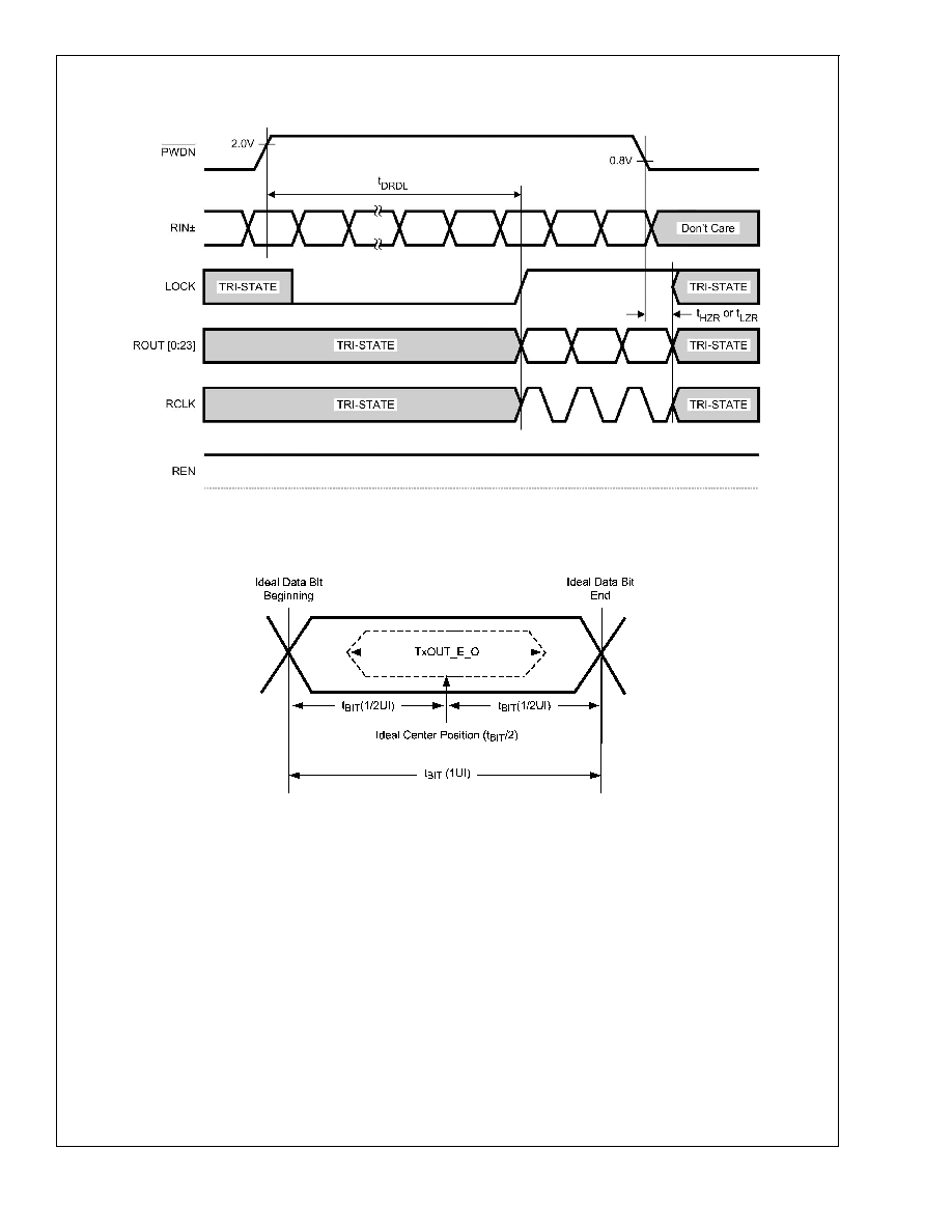
TxOUT_E_O
TxOUT_Eye_Opening
(respect to ideal)
5≠35 MHz
(Figure 14) (Notes 9, 13)
0.75
UI
(Note 10)
Deserializer Switching Characteristics
Over recommended operating supply and temperature ranges unless otherwise specified.
Symbol
Parameter
Conditions
Pin/Freq.
Min
Typ
Max
Units
t
RCP
Receiver out Clock Period
t
RCP
= t
TCP
(Note 8)
RCLK
28.6
200
ns
t
RDC
RCLK Duty Cycle
RCLK
45
50
55
%
t
CLH
LVCMOS Low-to-High
Transition Time
C
L
= 8 pF
(lumped load)
(Figure 4)
ROUT [23:0],
LOCK, RCLK
2.5
3.5
ns
t
CHL
LVCMOS High-to-Low
Transition Time
2.5
3.5
ns
t
ROS
ROUT (7:0) Setup Data to
RCLK (Group 1)
(Figure 11)
ROUT [7:0]
(0.40)*
t
RCP
(29/56)*t
RCP
ns
t
ROH
ROUT (7:0) Hold Data to
RCLK (Group 1)
(0.40)*
t
RCP
(27/56)*t
RCP
ns
t
ROS
ROUT (15:8) Setup Data to
RCLK (Group 2)
(Figure 11)
ROUT [15:8],
LOCK
(0.40)*
t
RCP
0.5*t
RCP
ns
t
ROH
ROUT (15:8) Hold Data to
RCLK (Group 2)
(0.40)*
t
RCP
0.5*t
RCP
ns
t
ROS
ROUT (23:16) Setup Data to
RCLK (Group 3)
(Figure 11)
ROUT [23:16]
(0.40)*
t
RCP
(27/56)*t
RCP
ns
t
ROH
ROUT (23:16) Hold Data to
RCLK (Group 3)
(0.40)*
t
RCP
(29/56)*t
RCP
ns
DS90C241/DS90C124
www.national.com
4
Deserializer Switching Characteristics
(Continued)
Over recommended operating supply and temperature ranges unless otherwise specified.
Symbol
Parameter
Conditions
Pin/Freq.
Min
Typ
Max
Units
t
HZR
HIGH to TRI-STATE Delay
(Figure 12)
ROUT [23:0],
RCLK, LOCK
3
10
ns
t
LZR
LOW to TRI-STATE Delay
3
10
ns
t
ZHR
TRI-STATE to HIGH Delay
3
10
ns
t
ZLR
TRI-STATE to LOW Delay
3
10
ns
t
DD
Deserializer Delay
(Figure 10)
RCLK
[4+(3/56)]T
+5.9
[4+(3/56)]T
+14
ns
t
DRDL
Deserializer PLL Lock Time
from Powerdown
(Figure 13)
(Notes 7, 8)
5 MHz
5
50
ms
35 MHz
5
50
ms
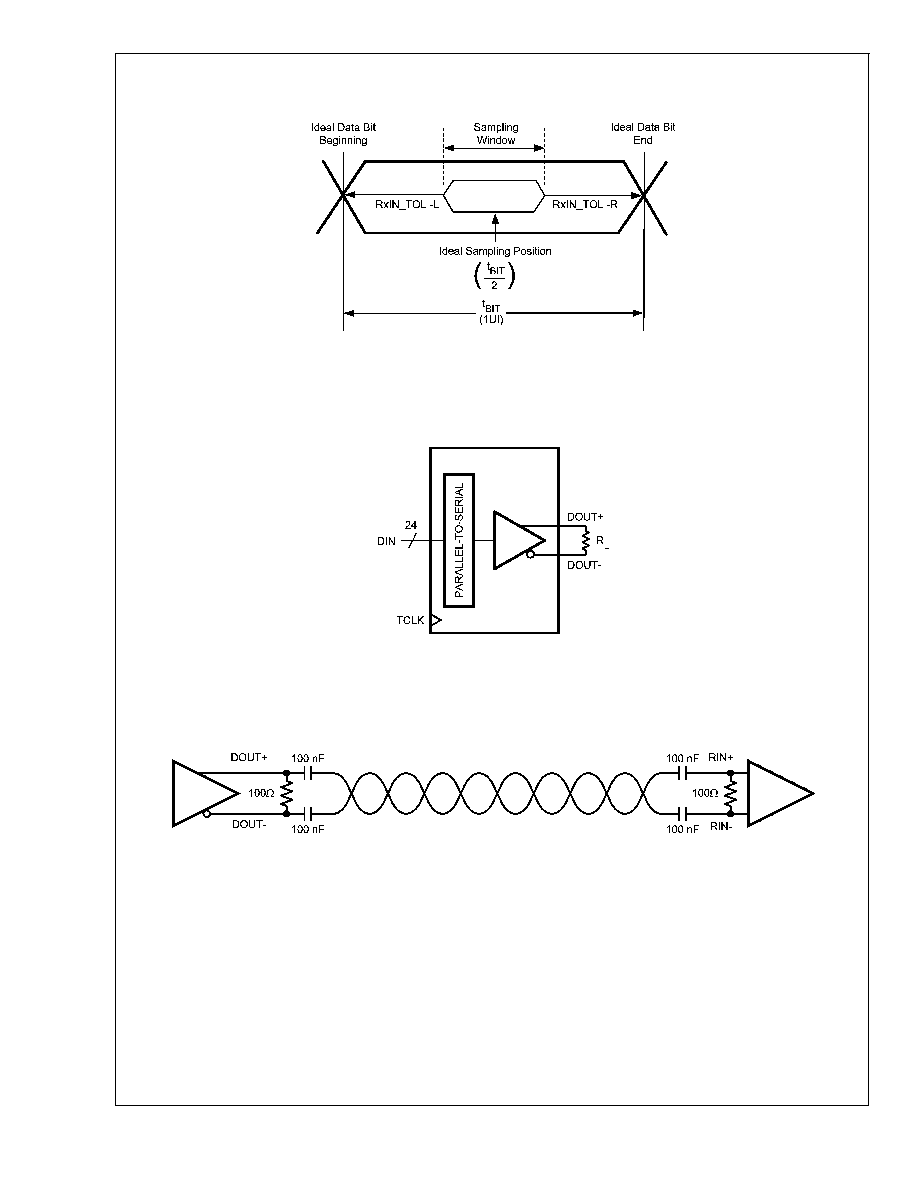
RxIN_TOL_L
Receiver INput TOLerance
Left,
(Figure 15)
(Notes 6, 10)
5 MHz≠35 MHz
0.25
UI
RxIN_TOL_R
Receiver INput TOLerance
Right,
(Figure 15)
(Notes 6, 10)
5 MHz≠35 MHz
0.25
UI
Note 1: "Absolute Maximum Ratings" are those values beyond which the safety of the device cannot be guaranteed. They are not meant to imply that the devices
should be operated at these limits. The table of "Electrical Characteristics" specifies conditions of device operation.
Note 2: Typical values are given for V
CC
= 3.3V and T
A
= +25∞C.
Note 3: Current into device pins is defined as positive. Current out of a device pin is defined as negative. Voltages are referenced to ground except VOD,
VOD,
VTH and VTL which are differential voltages.
Note 4: When the Serializer output is tri-stated, the Deserializer will lose PLL lock. Resynchronization MUST occur before data transfer.
Note 5: t
DRDL
is the time required by the deserializer to obtain lock when exiting powerdown mode. t
DRDL
is specified with an external synchronization pattern.
Note 6: RxIN_TOL is a measure of how much phase noise (jitter) the deserializer can tolerate in the incoming data stream before bit errors occur. It is a
measurement in reference with the ideal bit position, please see National's AN-1217 for detail.
Note 7: The Deserializer PLL lock time (t
DRDL
) may vary depending on input data patterns and the number of transitions within the pattern.
Note 8: Guaranteed by Design (GBD) using statistical analysis.
Note 9: t
JIT
(@BER of 10e-9) specifies the allowable jitter on TCLK. t
JIT
not included in TxOUT_E_O parameter.
Note 10: UI ≠ Unit Interval, equivalent to one ideal serialized data bit width. The UI scales with frequency.
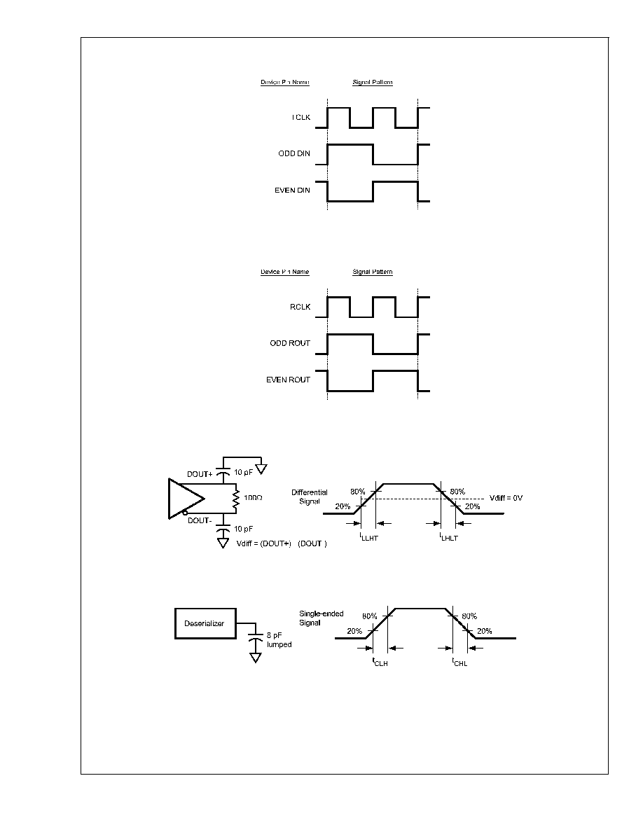
Note 11: Figures 1, 2, 9, 10, 13 show a falling edge data strobe (TCLK IN/RCLK OUT).
Note 12: Figures 6, 11 show a rising edge data strobe (TCLK IN/RCLK OUT).
Note 13: TxOUT_E_O is affected by pre-emphasis value.
DS90C241/DS90C124
www.national.com
5
AC Timing Diagrams and Test Circuits
20171902
FIGURE 1. Serializer Input Checker-board Pattern
20171903
FIGURE 2. Deserializer Output Checker-board Pattern
20171904
FIGURE 3. Serializer LVDS Output Load and Transition Times
20171905
FIGURE 4. Deserializer LVCMOS/LVTTL Output Load and Transition Times
DS90C241/DS90C124
www.national.com
6
AC Timing Diagrams and Test Circuits
(Continued)
20171906
FIGURE 5. Serializer Input Clock Transition Times
20171907
FIGURE 6. Serializer Setup/Hold Times
DS90C241/DS90C124
www.national.com
7

AC Timing Diagrams and Test Circuits
(Continued)
20171908
FIGURE 7. Serializer TRI-STATE Test Circuit and Delay
20171909
FIGURE 8. Serializer PLL Lock Time, and TPWDNB TRI-STATE Delays
DS90C241/DS90C124
www.national.com
8

AC Timing Diagrams and Test Circuits
(Continued)
20171910
FIGURE 9. Serializer Delay
20171911
FIGURE 10. Deserializer Delay
DS90C241/DS90C124
www.national.com
9

AC Timing Diagrams and Test Circuits
(Continued)
20171912
FIGURE 11. Deserializer Setup and Hold Times
20171913
Note: C
L
includes instrumentation and fixture capacitance within 6 cm of ROUT[23:0]
FIGURE 12. Deserializer TRI-STATE Test Circuit and Timing
DS90C241/DS90C124
www.national.com
10
AC Timing Diagrams and Test Circuits
(Continued)
20171914
FIGURE 13. Deserializer PLL Lock Times and RPWDNB TRI-STATE Delay
20171915
FIGURE 14. Transmitter Output Eye Opening (TxOUT_E_O)
DS90C241/DS90C124
www.national.com
11
AC Timing Diagrams and Test Circuits
(Continued)
20171916
RxIN_TOL_L is the ideal noise margin on the left of the figure, with respect to ideal.
RxIN_TOL_R is the ideal noise margin on the right of the above figure, with respect to ideal.
FIGURE 15. Receiver Input Tolerance (RxIN_TOL) and Sampling Window
20171917
VOD = (D
OUT+
) ≠ (D
OUT -
)
Differential output signal is shown as (D
OUT+
) ≠ (D
OUT -
), device in Data Transfer mode.
FIGURE 16. Serializer VOD Diagram
20171918
FIGURE 17. AC Coupled Application
DS90C241/DS90C124
www.national.com
12

Pin Descriptions
Pin #
Pin Name
I/O
Description
DS90C241 SERIALIZER PIN DESCRIPTIONS
22
VDDDR
VDD
Analog Voltage Supply, LVDS Output Power
21
VSSDR
GND
Analog Ground, LVDS Output Ground
16
VDDPT0
VDD
Analog Voltage supply, VCO Power
17
VSSPT0
GND
Analog Ground, VCO Ground
14
VDDPT1
VDD
Analog Voltage supply, PLL Power
15
VSSPT1
GND
Analog Ground, PLL Ground
30
VDDT
VDD
Digital Voltage supply, Tx Serializer Power
31
VSST
GND
Digital Ground, Tx Serializer Ground
7
VDDL
VDD
Digital Voltage supply, Tx Logic Power
6
VSSL
GND
Digital Ground, Tx Logic Ground
42
VDDIT
VDD
Digital Voltage supply, Tx Input Power
43
VSSIT
GND
Digital Ground, Tx Input Ground
24
VSS
GND
ESD Ground
4-1,
48-44,
41-32,
29-25
DIN[23:0]
CMOS_I
Transmitter Data INputs
10
TCLK
CMOS_I
Transmitter reference CLocK.
Used to strobe data at the DIN inputs and to drive the transmitter PLL
9
TPWDNB
CMOS_I
Transmitter PoWer DowN Bar (ACTIVE L).
TPWDNB = L; Disabled, DOUT (+/-) are TRI-STATED stand-by mode, PLL is shutdown
TPWDNB = H; Enabled
18
DEN
CMOS_I
Data ENable (ACTIVE H)
DEN = L; Disabled, DOUT (+/-) are TRI-STATED, PLL still operational
DEN = H; Enabled
13
RESRVD
CMOS_I
RESERVED - tie Low
23
PRE
CMOS_I
PRE-emphasis select pin.
PRE = (R
PRE
3 k); I
max
= [(1.2/R)*20], R
min
= 3 k
PRE = H or floating; pre-emphasis is disabled
11
TRFB
CMOS_I
Transmitter Rising/Falling Bar
TRFB = H; DIN LVCMOS Input clocked on Rising TCLK
TRFB = L; DIN LVCMOS Input clocked on Falling TCLK
12
VODSEL
CMOS_I
VOD level SELect
VODSEL = L; IOD
3.5 mA, (default). e.g. 3.5 mA*100350 mV
VODSEL = H; IOD
7.0 mA, VOD doubles approximately. e.g. 7 mA*100 700 mV
5
DCAOFF
CMOS_I
RESERVED -- tie Low
8
DCBOFF
CMOS_I
RESERVED -- tie Low
20
DOUT+
LVDS_O
Transmitter LVDS true (+) OUTput
19
DOUT-
LVDS_O
Transmitter LVDS inverted (-) OUTput
DS90C124 DESERIALIZER PIN DESCRIPTIONS
39
VDDIR
VDD
Analog LVDS Voltage supply, Power
40
VSSIR
GND
Analog LVDS Ground
47
VDDPR0
VDD
Analog Voltage supply, PLL Power
46
VSSPR0
GND
Analog Ground, PLL Ground
45
VDDPR1
VDD
Analog Voltage supply, PLL VCO Power
44
VSSPR1
GND
Analog Ground, PLL VCO Ground
37
VDDR1
VDD
Digital Voltage supply, Logic Power
38
VSSR1
GND
Digital Ground, Logic Ground
36
VDDR0
VDD
Digital Voltage supply, Logic Power
DS90C241/DS90C124
www.national.com
13
Pin Descriptions
(Continued)
Pin #
Pin Name
I/O
Description
DS90C124 DESERIALIZER PIN DESCRIPTIONS
35
VSSR0
GND
Digital Ground, Logic Ground
30
VDDOR1
VDD
Digital Voltage supply, LVCMOS Output Power
29
VSSOR1
GND
Digital Ground, LVCMOS Output Ground
20
VDDOR2
VDD
Digital Voltage supply, LVCMOS Output Power
19
VSSOR2
GND
Digital Ground, LVCMOS Output Ground
7
VDDOR3
VDD
Digital Voltage supply, LVCMOS Output Power
8
VSSOR3
GND
Digital Ground, LVCMOS Output Ground
41
RIN+
LVDS_I
Receiver LVDS true (+) INput
42
RIN-
LVDS_I
Receiver LVDS inverted (-) INput
2
RESRVD
CMOS_I
RESERVED - tie Low
43
RRFB
CMOS_I
Receiver Rising Falling Bar clock Edge Select
RRFB = H; ROUT LVCMOS Output clocked on Rising RCLK
RRFB = L; ROUT LVCMOS Output clocked on Falling RCLK
48
REN
CMOS_I
Receiver ENable, (ACTIVE H)
REN = L; Disabled, ROUT[23-0] and RCLK TRI-STATED, PLL still operational
REN = H; Enabled
1
RPWDNB
CMOS_I
Receiver PoWer DowN Bar (ACTIVE L)
RPWDNB = L; Disabled, ROUT[23-0], RCLK, and LOCK are TRI-STATED in stand-by
mode, PLL is shutdown
RPWDNB = H; Enabled
17
LOCK
CMOS_O
LOCK indicates the status of the receiver PLL
LOCK = L; receiver PLL is unlocked, ROUT[23-0] and RCLK are TRI-STATED
LOCK = H; receiver PLL is locked
25-28,
31-34
ROUT[7:0]
CMOS_O
Receiver LVCMOS level Outputs ≠ Group 1
13-16,
21-24
ROUT[15:8]
CMOS_O
Receiver LVCMOS level Outputs ≠ Group 2
3-6,
9-12
ROUT[23:16]
CMOS_O
Receiver LVCMOS level Outputs ≠ Group 3
18
RCLK
CMOS_O
Recovered CLocK. Parallel data rate clock recovered from the embedded clock. Used
to strobe ROUT, LVCMOS level output.
DS90C241/DS90C124
www.national.com
14

Pin Diagrams
Serializer - DS90C241
20171919
DS90C241/DS90C124
www.national.com
15

Pin Diagrams
(Continued)
Deserializer - DS90C124
20171920
DS90C241/DS90C124
www.national.com
16

Functional Description
The DS90C241 Serializer and DS90C124 Deserializer
chipset is an easy-to-use transmitter and receiver pair that
sends 24-bits of parallel LVCMOS data over a single serial
LVDS link from 120 Mbps to 840 Mbps throughput. The
DS90C241 transforms a 24-bit wide parallel LVCMOS data
into a single high speed LVDS serial data stream with em-
bedded clock. The DS90C124 receives the LVDS serial data
stream and converts it back into a 24-bit wide parallel data
and recovered clock. The 24-bit Serializer/Deserializer
chipset is designed to transmit data up to 10 meters over
shielded twisted pair (STP) at clock speeds from 5 MHz to 35
MHz.
The Deserializer can attain lock to a data stream without the
use of a separate reference clock source. The Deserializer
synchronizes to the Serializer regardless of data pattern,
delivering true automatic "plug and lock" performance. The
Deserializer recovers the clock and data by extracting the
embedded clock information and validating data integrity
from the incoming data stream and then deserializes the
data. The Deserializer monitors the incoming clock informa-
tion, determines lock status, and asserts the LOCK output
high when lock occurs. Each has a power down control to
enable efficient operation in various applications.
INITIALIZATION AND LOCKING MECHANISM
Initialization of the DS90C241 and DS90C124 must be es-
tablished before each device sends or receives data. Initial-
ization refers to synchronizing the Serializer's and Deserial-
izer's PLL's together. After the Serializers locks to the input
clock source, the Deserializer synchronizes to the Serializers
as the second and final initialization step.
Step 1: When V
CC
is applied to both Serializer and/or Dese-
rializer, the respective outputs are held in TRI-STATE and
internal circuitry is disabled by on-chip power-on circuitry.
When V
CC
reaches V
CC
OK (2.2V) the PLL in Serializer
begins locking to a clock input. For the Serializer, the local
clock is the transmit clock, TCLK. The Serializer outputs are
held in TRI-STATE while the PLL locks to the TCLK. After
locking to TCLK, the Serializer block is now ready to send
data patterns. The Deserializer output will remain in TRI-
STATE while its PLL locks to the embedded clock informa-
tion in serial data stream. Also, the Deserializer LOCK output
will remain low until its PLL locks to incoming data and
sync-pattern on the RIN
±
pins.
Step 2: The Deserializer PLL acquires lock to a data stream
without requiring the Serializer to send special patterns. The
Serializer that is generating the stream to the Deserializer
will automatically send random (non-repetitive) data patterns
during this step of the Initialization State. The Deserializer
will lock onto embedded clock within the specified amount of
time. An embedded clock and data recovery (CDR) circuit
locks to the incoming bit stream to recover the high-speed
receive bit clock and re-time incoming data. The CDR circuit
expects a coded input bit stream. In order for the Deserial-
izer to lock to a random data stream from the Serializer, it
performs a series of operations to identify the rising clock
edge and validates data integrity, then locks to it. Because
this locking procedure is independent on the data pattern,
total random locking duration may vary. At the point when the
Deserializer's CDR locks to the embedded clock, the LOCK
pin goes high and valid RCLK/data appears on the outputs.
Note that the LOCK signal is synchronous to valid data
appearing on the outputs. The Deserializer's LOCK pin is a
convenient way to ensure data integrity is achieved on re-
ceiver side.
DATA TRANSFER
After lock is established, the Serializer inputs DIN0≠DIN23
may be used to input data to the Serializer. Data is clocked
into the Serializer by the TCLK input. The edge of TCLK
used to strobe the data is selectable via the TRFB pin. TRFB
high selects the rising edge for clocking data and low selects
the falling edge. The Serializer outputs (DOUT
±
) are in-
tended to drive point-to-point connections or limited multi-
point applications.
CLK1, CLK0, DCA, DCB are four overhead bits transmitted
along the single LVDS serial data stream. The CLK1 bit is
always high and the CLK0 bit is always low. The CLK1 and
CLK0 bits function as the embedded clock bits in the serial
stream. DCB functions as the DC Balance control bit. It does
not require any pre-coding of data on transmit side. The DC
Balance bit is used to minimize the short and long-term DC
bias on the signal lines. This bit operates by selectively
sending the data either unmodified or inverted. The DCA bit
is used to validate data integrity in the embedded data
stream. Both DCA and DCB coding schemes are integrated
and automatically performed within Serializer and Deserial-
izer.
Serialized data and clock/control bits (24+4 bits) are trans-
mitted from the serial data output (DOUT
±
) at 28 times the
TCLK frequency. For example, if TCLK is 35 MHz, the serial
rate is 35 x 28 = 980 Mega bits per second. Since only 24
bits are from input data, the serial "payload" rate is 24 times
the TCLK frequency. For instance, if TCLK = 35 MHz, the
payload data rate is 35 x 24 = 840 Mbps. TCLK is provided
by the data source and must be in the range of 5 MHz to 35
MHz nominal. The Serializer outputs (DOUT
±
) can drive a
point-to-point connection. The outputs transmit data when
the enable pin (DEN) is high, TPWDNB is high. The DEN pin
may be used to TRI-STATE the outputs when driven low.
When the Deserializer channel attains lock to the input from
a Serializer, it drives its LOCK pin high and synchronously
delivers valid data and recovered clock on the output. The
Deserializer locks onto the embedded clock, uses it to gen-
erate multiple internal data strobes, and then drives the
recovered clock to the RCLK pin. The recovered clock
(RCLK output pin) is synchronous to the data on the
ROUT[23:0] pins. While LOCK is high, data on ROUT[23:0]
is valid. Otherwise, ROUT[23:0] is invalid. The polarity of the
RCLK edge is controlled by the RRFB input. ROUT(0-23),
LOCK and RCLK outputs will each drive a maximum of 8 pF
load with a 35 MHz clock. REN controls TRI-STATE for
ROUTn and the RCLK pin on the Deserializer.
RESYNCHRONIZATION
If the Deserializer loses lock, it will automatically try to re-
establish lock. For example, if the embedded clock edge is
not detected one time in succession, the PLL loses lock and
the LOCK pin is driven low. The Deserializer then enters the
operating mode where it tries to lock to a random data
stream. It looks for the embedded clock edge, identifies it
and then proceeds through the locking process. The logic
state of the LOCK signal indicates whether the data on
ROUT is valid; when it is high, the data is valid. The system
must monitor the LOCK pin to determine whether data on the
ROUT is valid. Because there is a short delay in the LOCK
signal's response to the PLL losing synchronization to the
incoming data stream, the system must determine the valid-
ity of data for the cycles before the LOCK signal goes high.
DS90C241/DS90C124
www.national.com
17

Functional Description
(Continued)
POWERDOWN
The Powerdown state is a low power sleep mode that the
Serializer and Deserializer may use to reduce power when
no data is being transferred. The TPWDNB and RPWDNB
are used to set each device into power down mode, which
reduces supply current to the µA range. The Serializer enters
powerdown when the TPWDNB pin is driven low. In power-
down, the PLL stops and the outputs go into TRI-STATE,
disabling load current and reducing supply. To exit Power-
down, TPWDNB must be driven high. When the Serializer
exits Powerdown, its PLL must lock to TCLK before it is
ready for the Initialization state. The system must then allow
time for Initialization before data transfer can begin. The
Deserializer enters powerdown mode when RPWDNB is
driven low. In powerdown mode, the PLL stops and the
outputs enter TRI-STATE. To bring the Deserializer block out
of the powerdown state, the system drives RPWDNB high.
Both the Serializer and Deserializer must reinitialize and
relock before data can be transferred. The Deserializer will
initialize and assert LOCK high until it is locked to the input
clock.
TRI-STATE
For the Serializer, TRI-STATE is entered when the DEN or
TPWDNB pin is driven low. This will TRI-STATE both driver
output pins (DOUT+ and DOUT-). When DEN is driven high,
the serializer will return to the previous state as long as all
other control pins remain static (TPWDNB, TRFB).
When you drive the REN or RPWDNB pin low, the Deseri-
alizer enters TRI-STATE. Consequently, the receiver output
pins (ROUT0≠ROUT23) and RCLK will enter TRI-STATE.
The LOCK output remains active, reflecting the state of the
PLL. The Deserializer input pins are high impedance during
receiver powerdown (RPWDNB low) and power-off (V
CC
=
0V).
PRE-EMPHASIS
The DS90C241 features a Pre-Emphasis mode used to
compensate for long or lossy transmission media. Cable
drive is enhanced with a user selectable Pre-Emphasis fea-
ture that provides additional output current during transitions
to counteract cable loading effects. The transmission dis-
tance will be limited by the loss characteristics and quality of
the media. Pre-Emphasis adds extra current during LVDS
logic transition to reduce the cable loading effects and in-
crease driving distance. In addition, Pre-Emphasis helps
provide faster transitions, increased eye openings, and im-
proved signal integrity. To enable the Pre-Emphasis function,
the "PRE" pin requires one external resistor (Rpre) to Vss in
order to set the additional current level. Pre-Emphasis
strength is set via an external resistor (Rpre) applied from
min to max (floating to 3k
) at the "PRE" pin. A lower input
resistor value on the "PRE" pin increases the magnitude of
dynamic current during data transition. There is an internal
current source based on the following formula: PRE = (Rpre
3k); I
MAX
= [(1.2/Rpre) X 20]. The ability of the
DS90C241 to use the Pre-Emphasis feature will extend the
transmission distance up to 10 meters in most cases.
AC-COUPLING AND TERMINATION
The DS90C241 and DS90C124 supports AC-coupled inter-
connects
through
integrated
DC
balanced
encoding/
decoding scheme. To use AC coupled connection between
the Serializer and Deserializer, insert external AC coupling
capacitors in series in the LVDS signal path as illustrated in
Figure 17. The Deserializer input stage is designed for AC-
coupling by providing a built-in AC bias network which sets
the internal V
CM
to +1.2V. With AC signal coupling, capaci-
tors provide the ac-coupling path to the signal input.
For the high-speed LVDS transmissions, the smallest avail-
able package should be used for the AC coupling capacitor.
This will help minimize degradation of signal quality due to
package parasitics. The most common used capacitor value
for the interface is 100 nF (0.1 uF) capacitor.
A termination resistor across DOUT
±
and RIN
±
is also
required for proper operation to be obtained. The termination
resistor should be equal to the differential impedance of the
media being driven. This should be in the range of 90 to 132
Ohms. 100 Ohms is a typical value common used with
standard 100 Ohm transmission media. This resistor is re-
quired for control of reflections and also to complete the
current loop. It should be placed as close to the Serializer
DOUT
±
outputs and Deserializer RIN
±
inputs to minimize
the stub length from the pins. To match with the deferential
impedance on the transmission line, the LVDS I/O are termi-
nated with 100 ohm resistors on Serializer DOUT
±
outputs
pins and Deserializer RIN
±
input pins.
PROGRESSIVE TURN≠ON (PTO)
Deserializer ROUT[23:0] outputs are grouped into three
groups of eight, with each group switching about 0.5UI apart
in phase to reduce EMI, simultaneous switching noise, and
system ground bounce.
Applications Information
USING THE DS90C241 AND DS90C124
The DS90C241/DS90C124 Serializer/Deserializer (SER-
DES) pair sends 24 bits of parallel LVCMOS data over a
serial LVDS link up to 840 Mbps. Serialization of the input
data is accomplished using an on-board PLL at the Serializer
which embeds clock with the data. The Deserializer extracts
the clock/control information from the incoming data stream
and deserializes the data. The Deserializer monitors the
incoming clockl information to determine lock status and will
indicate lock by asserting the LOCK output high.
POWER CONSIDERATIONS
An all CMOS design of the Serializer and Deserializer makes
them inherently low power devices. Additionally, the constant
current source nature of the LVDS outputs minimize the
slope of the speed vs. I
CC
curve of CMOS designs.
NOISE MARGIN
The Deserializer noise margin is the amount of input jitter
(phase noise) that the Deserializer can tolerate and still
reliably recover data. Various environmental and systematic
factors include:
Serializer: TCLK jitter, V
CC
noise (noise bandwidth and
out-of-band noise)
Media: ISI, V
CM
noise
Deserializer: V
CC
noise
For a graphical representation of noise margin, please see
Figure 15.
TRANSMISSION MEDIA
The Serializer and Deserializer can be used in point-to-point
configuration, through a PCB trace, or through twisted pair
cable. In a point-to-point configuration, the transmission me-
DS90C241/DS90C124
www.national.com
18

Applications Information
(Continued)
dia needs be terminated at both ends of the transmitter and
receiver pair. Interconnect for LVDS typically has a differen-
tial impedance of 100 Ohms. Use cables and connectors
that have matched differential impedance to minimize im-
pedance discontinuities. In most applications that involve
cables, the transmission distance will be determined on data
rates involved, acceptable bit error rate and transmission
medium.
HOT PLUG INSERTION
The Serializer and Deserializer devices support hot plug-
gable applications. The "Hot Inserted" operation on the serial
interface does not disrupt communication data on the active
data lines. The automatic receiver lock to random data "plug
& go" hot insertion capability allows the DS90C124 to attain
lock to the active data stream during a live insertion event.
PCB LAYOUT AND POWER SYSTEM
CONSIDERATIONS
Circuit board layout and stack-up for the LVDS SERDES
devices should be designed to provide low-noise power feed
to the device. Good layout practice will also separate high
frequency or high-level inputs and outputs to minimize un-
wanted stray noise pickup, feedback and interference.
Power system performance may be greatly improved by
using thin dielectrics (2 to 4 mils) for power / ground sand-
wiches. This arrangement provides plane capacitance for
the PCB power system with low-inductance parasitics, which
has proven especially effective at high frequencies, and
makes the value and placement of external bypass capaci-
tors less critical. External bypass capacitors should include
both RF ceramic and tantalum electrolytic types. RF capaci-
tors may use values in the range of 0.01 uF to 0.1 uF.
Tantalum capacitors may be in the 2.2 uF to 10 uF range.
Voltage rating of the tantalum capacitors should be at least
5X the power supply voltage being used.
Surface mount capacitors are recommended due to their
smaller parasitics. When using multiple capacitors per sup-
ply pin, locate the smaller value closer to the pin. A large bulk
capacitor is recommend at the point of power entry. This is
typically in the 50uF to 100uF range and will smooth low
frequency switching noise. It is recommended to connect
power and ground pins directly to the power and ground
planes with bypass capacitors connected to the plane with
via on both ends of the capacitor. Connecting power or
ground pins to an external bypass capacitor will increase the
inductance of the path.
A small body size X7R chip capacitor, such as 0603, is
recommended for external bypass. Its small body size re-
duces the parasitic inductance of the capacitor. The user
must pay attention to the resonance frequency of these
external bypass capacitors, usually in the range of 20-30
MHz range. To provide effective bypassing, multiple capaci-
tors are often used to achieve low impedance between the
supply rails over the frequency of interest. At high frequency,
it is also a common practice to use two vias from power and
ground pins to the planes, reducing the impedance at high
frequency.
Some devices provide separate power and ground pins for
different portions of the circuit. This is done to isolate switch-
ing noise effects between different sections of the circuit.
Separate planes on the PCB are typically not required. Pin
Description tables typically provide guidance on which circuit
blocks are connected to which power pin pairs. In some
cases, an external filter many be used to provide clean
power to sensitive circuits such as PLLs.
Use at least a four layer board with a power and ground
plane. Locate LVCMOS (LVTTL) signals away from the
LVDS lines to prevent coupling from the CMOS lines to the
LVDS lines. Closely-coupled differential lines of 100 Ohms
are typically recommended for LVDS interconnect. The
closely coupled lines help to ensure that coupled noise will
appear as common-mode and thus is rejected by the receiv-
ers. The tightly coupled lines will also radiate less.
Termination of the LVDS interconnect is required. For point-
to-point applications, termination should be located at both
ends of the devices. Nominal value is 100 Ohms to match
the line's differential impedance. Place the resistor as close
to the transmitter DOUT
±
outputs and receiver RIN
±
inputs
as possible to minimize the resulting stub between the ter-
mination resistor and device.
LVDS INTERCONNECT GUIDELINES
See AN-1108 and AN-905 for full details.
∑
Use 100
coupled differential pairs
∑
Use the S/2S/3S rule in spacings
-- S = space between the pair
-- 2S = space between pairs
-- 3S = space to LVCMOS/LVTTL signal
∑
Minimize the number of VIA
∑
Use differential connectors when operating above
500Mbps line speed
∑
Maintain balance of the traces
∑
Minimize skew within the pair
∑
Terminate as close to the TX outputs and RX inputs as
possible
Additional general guidance can be found in the LVDS Own-
er's Manual - available in PDF format from the National web
site at: www.national.com/lvds
DS90C241/DS90C124
www.national.com
19
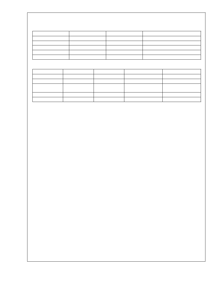
Truth Tables
TABLE 1. DS90C241 Serializer Truth Table
Pin 9
Pin 18
(Internal)
Pins 19 and 20
TPWDNB
DEN
Tx PLL Status
LVDS Outputs
L
X
X
Hi Z
H
L
X
Hi Z
H
H
Not Locked
Hi Z
H
H
Locked
Serialized Data with Embedded Clock
TABLE 2. DS90C124 Deserializer Truth Table
Pin 1
Pin 48
(Internal)
(See Pin Diagram)
Pin 17
RPWDNB
REN
Rx PLL Status
ROUTn and RCLK
LOCK
L
X
X
Hi Z
Hi Z
H
L
X
Hi Z
L = PLL Unocked;
H = PLL Locked
H
H
Not Locked
Hi Z
L
H
H
Locked
Data and RCLK Active
H
DS90C241/DS90C124
www.national.com
20

Physical Dimensions
inches (millimeters) unless otherwise noted
Dimensions show in millimeters only
NS Package Number IVS48
Ordering Information
NSID
Package Type
Package ID
DS90C241
48 Lead TQFP style, 7.0 X 7.0 X 1.0 mm, 0.5 mm pitch, DS90C241IVS
IVS48
DS90C241
48 Lead TQFP style, 7.0 X 7.0 X 1.0 mm, 0.5 mm pitch, 1000 std reel, DS90C241IVSX
IVS48
DS90C124
48 Lead TQFP style, 7.0 X 7.0 X 1.0 mm, 0.5 mm pitch, DS90C124IVS
IVS48
DS90C124
48 Lead TQFP style, 7.0 X 7.0 X 1.0 mm, 0.5 mm pitch, 1000 std reel, DS90C124IVSX
IVS48
National does not assume any responsibility for use of any circuitry described, no circuit patent licenses are implied and National reserves
the right at any time without notice to change said circuitry and specifications.
For the most current product information visit us at www.national.com.
LIFE SUPPORT POLICY
NATIONAL'S PRODUCTS ARE NOT AUTHORIZED FOR USE AS CRITICAL COMPONENTS IN LIFE SUPPORT DEVICES OR SYSTEMS
WITHOUT THE EXPRESS WRITTEN APPROVAL OF THE PRESIDENT AND GENERAL COUNSEL OF NATIONAL SEMICONDUCTOR
CORPORATION. As used herein:
1. Life support devices or systems are devices or systems
which, (a) are intended for surgical implant into the body, or
(b) support or sustain life, and whose failure to perform when
properly used in accordance with instructions for use
provided in the labeling, can be reasonably expected to result
in a significant injury to the user.
2. A critical component is any component of a life support
device or system whose failure to perform can be reasonably
expected to cause the failure of the life support device or
system, or to affect its safety or effectiveness.
BANNED SUBSTANCE COMPLIANCE
National Semiconductor follows the provisions of the Product Stewardship Guide for Customers (CSP-9-111C2) and Banned Substances
and Materials of Interest Specification (CSP-9-111S2) for regulatory environmental compliance. Details may be found at:
www.national.com/quality/green.
Lead free products are RoHS compliant.
National Semiconductor
Americas Customer
Support Center
Email: new.feedback@nsc.com
Tel: 1-800-272-9959
National Semiconductor
Europe Customer Support Center
Fax: +49 (0) 180-530 85 86
Email: europe.support@nsc.com
Deutsch Tel: +49 (0) 69 9508 6208
English
Tel: +44 (0) 870 24 0 2171
FranÁais Tel: +33 (0) 1 41 91 8790
National Semiconductor
Asia Pacific Customer
Support Center
Email: ap.support@nsc.com
National Semiconductor
Japan Customer Support Center
Fax: 81-3-5639-7507
Email: jpn.feedback@nsc.com
Tel: 81-3-5639-7560
www.national.com
DS90C241/DS90C124
5-35MHz
DC-Balanced
24-Bit
L
VDS
Serializer
and
Deserializer