DS90C363A/DS90CF363A
+3.3V Programmable LVDS Transmitter 18-Bit Flat Panel
Display (FPD) Link -65 MHz
+3.3VLVDS Transmitter 18-Bit Flat Panel Display (FPD)
Link -65 MHz
General Description
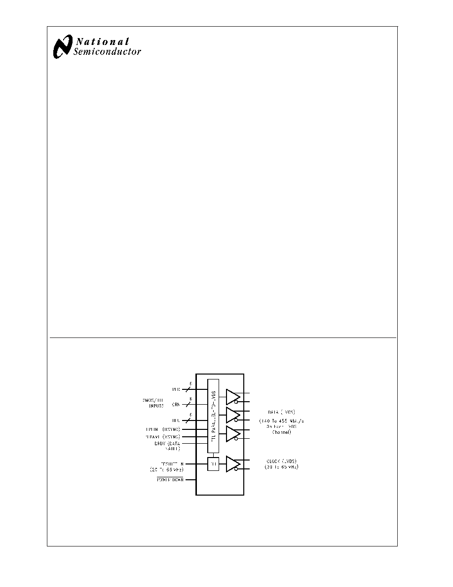
The DS90C363A/DS90CF363A transmitter converts 21 bits
of CMOS/TTL data into three LVDS (Low Voltage Differential
Signaling) data streams. A phase-locked transmit clock is
transmitted in parallel with the data streams over a fourth
LVDS link. Every cycle of the transmit clock 21 bits of input
data are sampled and transmitted. At a transmit clock fre-
quency of 65 MHz, 18 bits of RGB data and 3 bits of LCD
timing and control data (FPLINE, FPFRAME, DRDY) are
transmitted at a rate of 455 Mbps per LVDS data channel.
Using a 65 MHz clock, the data throughput is 170 Mbytes/
sec. The DS90C363A transmitter can be programmed for
Rising edge strobe or Falling edge strobe through a dedi-
cated pin. The DS90CF363A is fixed as a Falling edge
strobe transmitter. A Rising edge or Falling edge strobe
transmitter will interoperate with a Falling edge strobe Re-
ceiver (DS90CF364) without any translation logic.
This chipset is an ideal means to solve EMI and cable size
problems associated with wide, high speed TTL interfaces.
Features
n
20 to 65 MHz shift clock support
n
Rejects
>
�
3ns Jitter from VGA chip with less than
225ps output Jitter
@
65MHz (TJCC)
n
Best�in�Class Set & Hold Times on TxINPUTs
n
Tx power consumption
<
130 mW (typ)
@
65MHz
Grayscale
n
>
50% Less Power Dissipation than BiCMOS
Alternatives
n
Tx Power-down mode
<
200�W (max)
n
ESD rating
>
7 kV (HBM),
>
500V (EIAJ)
n
Supports VGA, SVGA, XGA and Dual Pixel SXGA.
n
Narrow bus reduces cable size and cost
n
Up to 1.3 Gbps throughput
n
Up to 170 Megabytes/sec bandwidth
n
345 mV (typ) swing LVDS devices for low EMI
n
PLL requires no external components
n
Compatible with TIA/EIA-644 LVDS standard
n
Low profile 48-lead TSSOP package
n
Improved replacement for:
SN75LVDS85 -- DS90C363A
SN75LVDS84 -- DS90CF363A
Block Diagram
DS90C363A/DS90CF363A
10013801
Order Number DS90C363AMTD or DS90CF363AMTD
See NS Package Number MTD48
TRI-STATE
�
is a registered trademark of National Semiconductor Corporation.
May 2003
+3.3V
Programmable
L
VDS
T
ransmitter
18-Bit
Flat
Panel
Display
(FPD)
Link
-65
MHz
+3.3VL
VDS
T
ransmitter
18-Bit
Flat
Panel
Display
(FPD)
Link
-65
MHz
� 2003 National Semiconductor Corporation
DS100138
www.national.com
Absolute Maximum Ratings
(Note 1)
If Military/Aerospace specified devices are required,
please contact the National Semiconductor Sales Office/
Distributors for availability and specifications.
Supply Voltage (V
CC
)
-0.3V to +4V
CMOS/TTL Input Voltage
-0.3V to (V
CC
+ 0.3V)
LVDS Driver Output Voltage
-0.3V to (V
CC
+ 0.3V)
LVDS Output Short Circuit
Duration
Continuous
Junction Temperature
+150�C
Storage Temperature
-65�C to +150�C
Lead Temperature
(Soldering, 4 sec)
+260�C
Maximum Package Power Dissipation Capacity
@
25�C
MTD48 (TSSOP) Package:
DS90C363A/DS90CF363A
1.98 W
Package Derating:
DS90C363A/DS90CF363A
16 mW/�C above +25�C
ESD Rating
(HBM, 1.5 k
, 100 pF)
>
7 kV
(EIAJ, 0
, 200 pF)
>
500V
Recommended Operating
Conditions
Min Nom Max
Units
Supply Voltage (V
CC
)
3.0
3.3
3.6
V
Operating Free Air
Temperature (T
A
)
-10 +25 +70
�C
Receiver Input Range
0
2.4
V
Supply Noise Voltage (V
CC
)
100
mV
PP
TxCLKIN frequency
18
68
MHz
Electrical Characteristics
Over recommended operating supply and temperature ranges unless otherwise specified.
Symbol
Parameter
Conditions
Min
Typ
Max
Units
CMOS/TTL DC SPECIFICATIONS
V
IH
High Level Input Voltage
2.0
V
CC
V
V
IL
Low Level Input Voltage
GND
0.8
V
V
CL
Input Clamp Voltage
I
CL
= -18 mA
-0.79
-1.5
V
I
IN
Input Current
V
IN
= 0.4V, 2.5V or V
CC
+1.8
+10
�A
V
IN
= GND
-10
0
�A
LVDS DC SPECIFICATIONS
V
OD
Differential Output Voltage
R
L
= 100
250
345
450
mV
V
OD
Change in V
OD
between
complimentary output states
35
mV
V
OS
Offset Voltage (Note 4)
1.125
1.25
1.375
V
V
OS
Change in V
OS
between
complimentary output states
35
mV
I
OS
Output Short Circuit Current
V
OUT
= 0V, R
L
= 100
-3.5
-5
mA
I
OZ
Output TRI-STATE
�
Current
Power Down = 0V,
V
OUT
= 0V or V
CC
�
1
�
10
�A
TRANSMITTER SUPPLY CURRENT
ICCTW
Transmitter Supply Current
Worst Case
R
L
= 100
,
C
L
= 5 pF,
Worst Case Pattern
(Figures 1, 4 )
f = 32.5 MHz
31
43
mA
f = 37.5 MHz
33
45
mA
f = 65 MHz
39
52
mA
ICCTG
Transmitter Supply Current
16 Grayscale
R
L
= 100
,
C
L
= 5 pF,
16 Grayscale Pattern
(Figures 2, 4 )
f = 32.5 MHz
23
35
mA
f = 37.5 MHz
28
40
mA
f = 65 MHz
33
45
mA
ICCTZ
Transmitter Supply Current
Power Down
Power Down = Low
Driver Outputs in TRI-STATE
�
under
Power Down Mode
10
55
�A
Note 1: "Absolute Maximum Ratings" are those values beyond which the safety of the device cannot be guaranteed. They are not meant to imply that the device
should be operated at these limits. The tables of "Electrical Characteristics" specify conditions for device operation.
Note 2: Typical values are given for V
CC
= 3.3V and T
A
= +25C.
Note 3: Current into device pins is defined as positive. Current out of device pins is defined as negative. Voltages are referenced to ground unless otherwise
specified (except V
OD
and
V
OD
).
Note 4: V
OS
previously referred as V
CM
.
DS90C363A/DS90CF363A
www.national.com
2
Recommended Transmitter Input Characteristics
Over recommended operating supply and temperature ranges unless otherwise specified
Symbol
Parameter
Min
Typ
Max
Units
TCIT
TxCLK IN Transition Time (Figure 5 )
5
ns
TCIP
TxCLK IN Period (Figure 6 )
14.7
T
55.6
ns
TCIH
TxCLK IN High Time (Figure 6 )
0.35T
0.5T
0.65T
ns
TCIL
TxCLK IN Low Time (Figure 6 )
0.35T
0.5T
0.65T
ns
Transmitter Switching Characteristics
Over recommended operating supply and temperature ranges unless otherwise specified
Symbol
Parameter
Min
Typ
Max
Units
LLHT
LVDS Low-to-High Transition Time (Figure 4 )
0.75
1.5
ns
LHLT
LVDS High-to-Low Transition Time (Figure 4 )
0.75
1.5
ns
TPPos0
Transmitter Output Pulse Position for Bit 0 (Figure 11 ) (Note 5)
f = 65 MHz
-0.30
0
0.20
ns
TPPos1
Transmitter Output Pulse Position for Bit 1
1.90
2.20
2.40
ns
TPPos2
Transmitter Output Pulse Position for Bit 2
4.10
4.40
4.60
ns
TPPos3
Transmitter Output Pulse Position for Bit 3
6.30
6.60
6.80
ns
TPPos4
Transmitter Output Pulse Position for Bit 4
8.50
8.80
9.00
ns
TPPos5
Transmitter Output Pulse Position for Bit 5
10.70
11.00
11.20
ns
TPPos6
Transmitter Output Pulse Position for Bit 6
12.90
13.20
13.40
ns
TPPos0
Transmitter Output Pulse Position for Bit 0 (Figure 11 ) (Note 5)
f = 40 MHz
-0.35
0
0.35
ns
TPPos1
Transmitter Output Pulse Position for Bit 1
3.22
3.57
3.92
ns
TPPos2
Transmitter Output Pulse Position for Bit 2
6.79
7.14
7.49
ns
TPPos3
Transmitter Output Pulse Position for Bit 3
10.36
10.71
11.06
ns
TPPos4
Transmitter Output Pulse Position for Bit 4
13.93
14.28
14.63
ns
TPPos5
Transmitter Output Pulse Position for Bit 5
17.51
17.86
18.21
ns
TPPos6
Transmitter Output Pulse Position for Bit 6
21.08
21.43
21.78
ns
TPPos0
Transmitter Output Pulse Position for Bit 0 (Figure 11 ) (Note 5)
f = 32.5 MHz
-0.40
0
0.40
ns
TPPos1
Transmitter Output Pulse Position for Bit 1
4.00
4.40
4.80
ns
TPPos2
Transmitter Output Pulse Position for Bit 2
8.40
8.80
9.20
ns
TPPos3
Transmitter Output Pulse Position for Bit 3
12.80
13.20
13.60
ns
TPPos4
Transmitter Output Pulse Position for Bit 4
17.20
17.60
18.00
ns
TPPos5
Transmitter Output Pulse Position for Bit 5
21.60
22.00
22.40
ns
TPPos6
Transmitter Output Pulse Position for Bit 6
26.00
26.40
26.80
ns
TSTC
TxIN Setup to TxCLK IN (Figure 6 )
2.5
ns
THTC
TxIN Hold to TxCLK IN (Figure 6 )
0
ns
TCCD
TxCLK IN to TxCLK OUT Delay (Figure 7 ) T
A
=25�C, V
CC
=3.3V
3
5.5
ns
TxCLK IN to TxCLK OUT Delay (Figure 7 )
3
7.0
ns
TJCC
Transmitter Jitter Cycle-to-Cycle (Figures 12, 13 ) (Note 6)
f = 65 MHz
175
225
ps
f = 40 MHz
240
380
ps
f = 32.5 MHz
260
400
ps
TPLLS
Transmitter Phase Lock Loop Set (Figure 8 )
10
ms
TPDD
Transmitter Power Down Delay (Figure 10 )
100
ns
Note 5: The Minimum and Maximum Limits are based on statistical analysis of the device performance over process, voltage, and temperature ranges. This
parameter is functionality tested only on Automatic Test Equipment (ATE).
Note 6: The Limits are based on statistical analysis of the device performance over process, voltage, and temperature ranges. Output jitter is measured with a
cycle-to-cycle jitter of 3ns applied to the input clock signal. A jitter event of 3ns, represents worse case jump in the clock edge from most Graphics controller VGA
chips currently available. This parameter is used when calculating system margin (RSKM). See Figures 12, 13 and AN-1059.
DS90C363A/DS90CF363A
www.national.com
3
AC Timing Diagrams
Note 7: The worst case test pattern produces a maximum toggling of digital circuits, LVDS I/O and CMOS/TTL I/O.
Note 8: The 16 grayscale test pattern tests device power consumption for a "typical" LCD display pattern. The test pattern approximates signal switching needed
to produce groups of 16 vertical stripes across the display.
Note 9: Figures 1, 2 show a falling edge data strobe (TxCLK IN/RxCLK OUT).
Note 10: Recommended pin to signal mapping. Customer may choose to define differently.
10013804
FIGURE 1. "Worst Case" Test Pattern
10013805
FIGURE 2. "16 Grayscale" Test Pattern (Notes 7, 8, 9, 10)
10013830
FIGURE 3. DS90C363A/DS90CF363A (Transmitter) LVDS Output Load
DS90C363A/DS90CF363A
www.national.com
4
AC Timing Diagrams
(Continued)
10013806
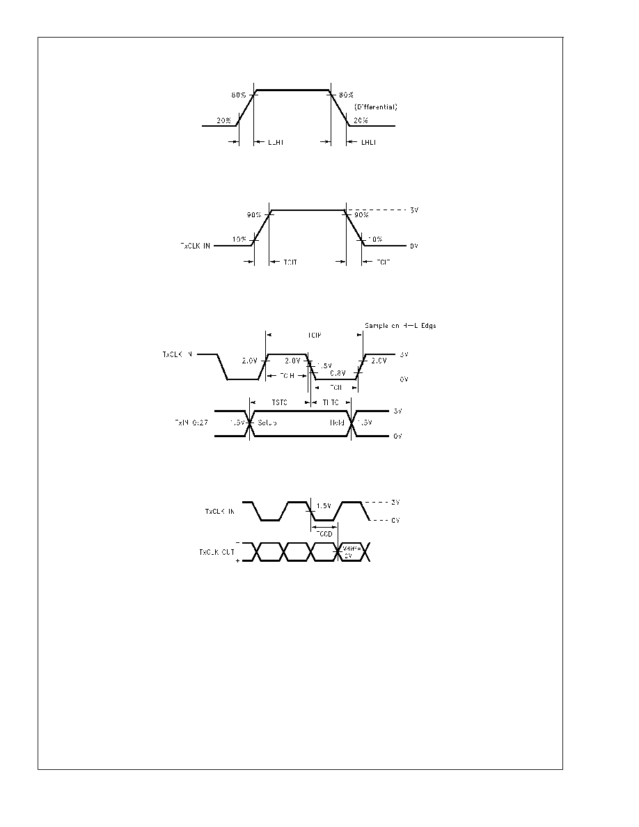
FIGURE 4. DS90C363A/DS90CF363A (Transmitter) LVDS Transition Times
10013808
FIGURE 5. DS90C363A/DS90CF363A (Transmitter) Input Clock Transition Time
10013810
FIGURE 6. DS90C363A/DS90CF363A (Transmitter) Setup/Hold and High/Low Times (Falling Edge Strobe)
10013812
FIGURE 7. DS90C363A/DS90CF363A (Transmitter) Clock In to Clock Out Delay (Falling Edge Strobe)
DS90C363A/DS90CF363A
www.national.com
5