DS90C387R
85MHz Dual 12-Bit Double Pumped Input LDI Transmitter
- VGA/UXGA
General Description
The DS90C387R transmitter is designed to support pixel
data transmission from a Host to a Flat Panel Display up to
UXGA resolution. It is designed to be compatible with Graph-
ics Memory Controller Hub( GMCH) by implementing two
data per clock and can be controlled by a two-wire serial
communication interface. Two input modes are supported:
one port of 12-bit( two data per clock) input for 24-bit RGB,
and two ports of 12-bit( two data per clock) input for dual
24-bit RGB( 48-bit total). In both modes, input data will be
clocked on both rising and falling edges in LVTTL level
operation, or clocked on the cross over of differential clock
signals in the low swing operation. Each input data width will
be 1/2 of clock cycle. With an input clock at 85MHz and input
data at 170Mbps, the maximum transmission rate of each
LVDS line is 595Mbps, for a aggregate throughput rate of
2.38Gbps/4.76Gbps. It converts 24/48 bits (Single/Dual
Pixel 24-bit color) of data into 4/8 LVDS (Low Voltage Differ-
ential Signaling) data streams. DS90C387R can be pro-
grammed via the two-wire serial communication interface.
The LVDS output pin-out is identical to DS90C387. Thus,
this transmitter can be paired up with DS90CF388, receiver
of the 112MHz LDI chipset or FPD-Link Receivers in non-DC
Balance mode operation which provides GUI/LCD panel/
mother board vendors a wide choice of inter-operation with
LVDS based TFT panels.
DS90C387R also comes with features that can be found on
DS90C387. Cable drive is enhanced with a user selectable
pre-emphasis feature that provides additional output current
during transitions to counteract cable loading effects. DC
Balancing on a cycle-to-cycle basis is also provided to re-
duce ISI( Inter-Symbol Interference), control signals (
VSYNC, HSYNC, DE) are sent during blanking intervals.
With pre-emphasis and DC Balancing, a low distortion eye-
pattern is provided at the receiver end of the cable. These
enhancements allow cables 5 to 15+ meters in length to be
driven depending on media characteristic and pixel clock
speed. Pre-emphasis is available in both the DC Balanced
and Non-DC Balanced modes. In the Non-DC Balanced
mode backward compatibility with FPD-Link Receivers is
obtained.
This chip is an ideal solution to solve EMI and cable size
problems for high-resolution flat panel display applications. It
provides a reliable industry standard interface based on
LVDS technology that delivers the bandwidth needed for
high-resolution panels while maximizing bit times, and keep-
ing clock rates low to reduce EMI and shielding require-
ments. For more details, please refer to the "Applications
Information" section of this datasheet.
Features
n
Complies with Open LDI specification for digital display
interfaces
n
25 to 85MHz clock support
n
Supports VGA through UXGA panel resolution
n
Up to 4.76Gbps bandwidth in dual 24-bit RGB in-to-dual
pixel out application.
n
Dual 12-bit Double Pumped Input DVO port.
n
Pre-emphasis reduces cable loading effects.
n
Drives long, low cost cables
n
DC Balance data transmission provided by transmitter
reduces ISI distortion
n
Transmitter rejects cycle-to-cycle jitter.(+/- 2ns of input
bit period)
n
Support both LVTTL and low voltage level input(capable
of 1.0 to 1.8V)
n
Two-wire serial communication interface up to 400 KHz
n
Programmable input clock and control strobe select
n
Backward compatible configuration with 112MHz LDI
and FPD-Link.
n
Optional second LVDS clock for backward compatibility
w/ FPD-Link Receivers
n
Compatible with TIA/EIA-644
TRI-STATE
�
is a registered trademark of National Semiconductor Corporation.
December 2003
DS90C387R
85MHz
Dual
12-Bit
Double
Pumped
Input
LDI
T
ransmitter
-
VGA/UXGA
� 2003 National Semiconductor Corporation
DS101288
www.national.com
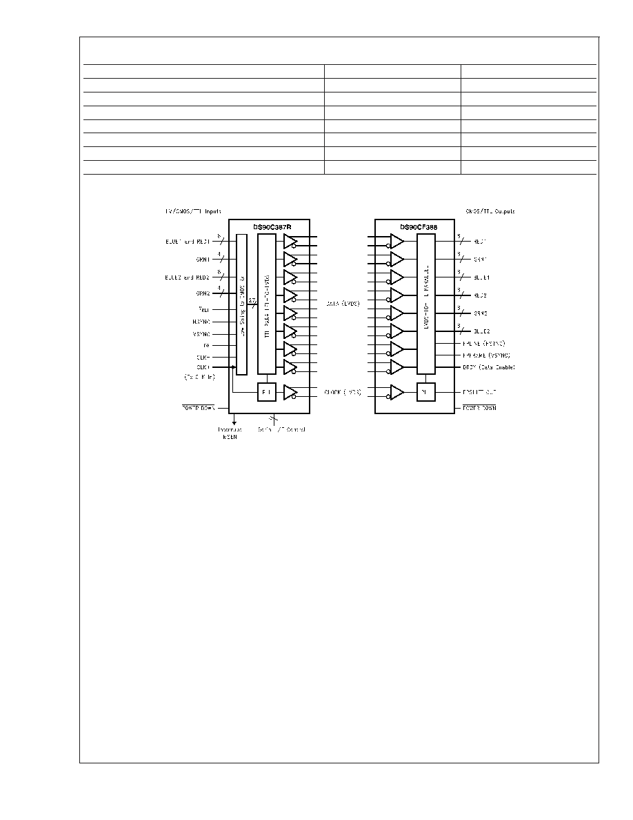
Mode Configuration / PerformanceTable
Mode
one 12-bit
two 12-bit
Mode (GUI Out/Cable)
single/single
dual/dual
Input Clock Rate (MHz)
25-85
25-85
Input Data Rate (Mbps)
50-170
50-170
LVDS data Pairs Out
4
8
Ouput Clock Rate (MHz)
25-85
25-85
Data Rate Out (Mbps) per LVDS channel
175-595
175-595
Throughput Data Rate Out
2.38Gbps
4.76Gbps
Generalized Block Diagrams
10128801
DS90C387R
www.national.com
2
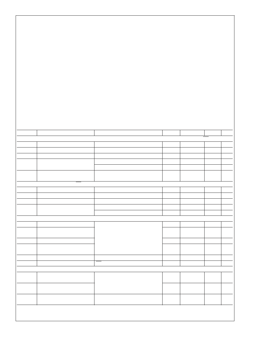
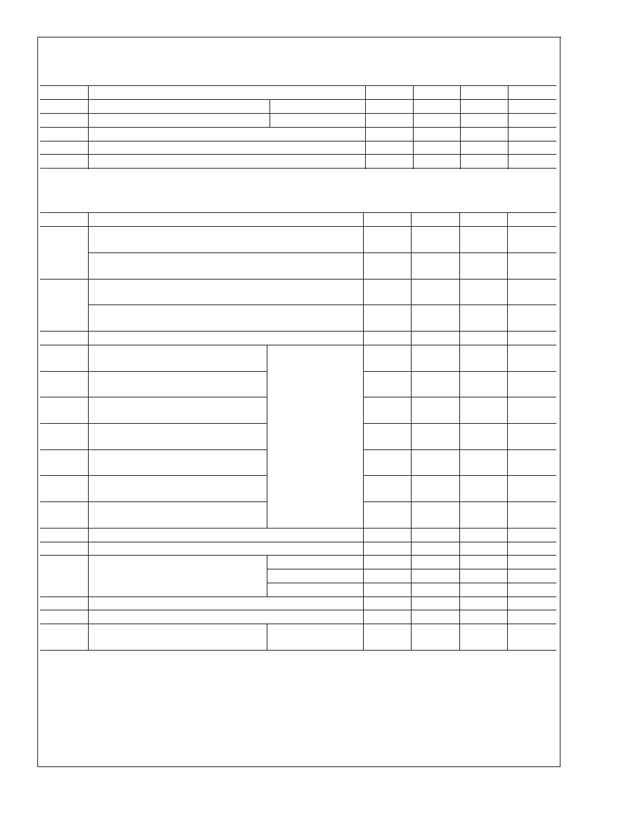
Absolute Maximum Ratings
(Note 1)
If Military/Aerospace specified devices are required,
please contact the National Semiconductor Sales Office/
Distributors for availability and specifications.
Supply Voltage (V
CC
)
-0.3V to +4V
LVCMOS/LVTTL Output
Voltage
-0.3V to (V
CC
+ 0.3V)
LVDS Driver Output
Voltage
-0.3V to (V
CC
+ 0.3V)
LVDS Output Short
Circuit
Duration
Continuous
Junction Temperature
+150�C
Storage Temperature
-65�C to +150�C
Lead Temperature
(Soldering, 4 sec.)
+260�C
Maximum Package Power Dissipation Capacity
@
25�C
100 TQFP Package:
2.8W
Package Derating:
DS90C387R
18.2mW/�C above +25�C
ESD Rating:
(HBM, 1.5k
, 100pF)
>
2 kV
(EIAJ, 0
, 200pF)
>
300 V
Recommended Operating
Conditions
Min
Nom
Max
Units
All Supply Voltage
3.0
3.3
3.6
V
Operating Free Air
Temperature (T
A)
-10
+25
+70
�C
Supply Noise Voltage (V
CC
)up
to 33MHz
100 mV
p-p
Electrical Characteristics
Over recommended operating supply and temperature ranges unless otherwise specified.(Note 2)
Symbol
Parameter
Conditions
Min
Typ
Max
Units
LVCMOS/LVTTL DC SPECIFICATIONS ( All pins, except output pins AnP, AnM, CLKnP and CLKnM, BAL, PD pins)
V
IH
High Level Input Voltage
V
REF
= V
CC3V
= V
CC
2.0
V
CC
V
V
IL
Low Level Input Voltage
V
REF
= V
CC3V
= V
CC
GND
0.8
V
V
CL
Input Clamp Voltage
I
CL
= 18 mA
-0.8
-1.5
V
I
IN
Input Current
V
IN
= 0.4V, or V
CC
+1.8
+15
�A
V
IN
= GND
-15
0
�A
V
OL
Low level Open Drain Output
Voltage
I
OL
= 2 mA
0.1
0.3
V
LVCMOS DC SPECIFICATIONS ( PD pin)
V
IH
High Level Input Voltage
V
REF
= V
CC3V
= V
CC
2.9
V
CC
V
V
IL
Low Level Input Voltage
V
REF
= V
CC3V
= V
CC
GND
0.8
V
V
CL
Input Clamp Voltage
I
CL
= 18 mA
-0.8
-1.5
V
I
IN
Input Current
V
IN
= 0.4V, or V
CC
+1.8
+15
�A
V
IN
= GND
-15
0
�A
LVDS DRIVER DC SPECIFICATIONS (output pins AnP, AnM, CLKnP and CLKnM)
V
OD
Differential Output Voltage
R
L
= 100
247
345
550
mV
V
OD
Change in V
OD
between
Complimentary Output States
35
mV
V
OS
Offset Voltage
1.125
1.25
1.475
V
V
OS
Change in V
OS
between
Complimentary Output States
35
mV
I
OS
Output Short Circuit Current
V
OUT
= 0V, R
L
= 100
-3.5
-11
mA
I
OZ
Output TRI-STATE
�
Current
PD = 0V, V
OUT
= 0V or V
CC
�
1
�
10
�A
Low Voltage Mode DC SPECIFICATIONS( pins D0 to D23, CLKINP, CLKINM, DE, HSYNC,VSYNC)
V
IHLS
Low Swing High Level Input
Voltage, V
CC
= 3V
V
REF
+100mV
1.8
V
V
ILLS
Low Swing Low Level Input
Voltage,V
CC
= 3V
GND
V
REF
-100mV
V
V
REF
Differential Input Reference
Voltage, V
CC
= 3V
Low Swing,V
REF
=
1
/
2
V
DDQ
0.45
0.5*V
DDQ
1
V
DS90C387R
www.national.com
3
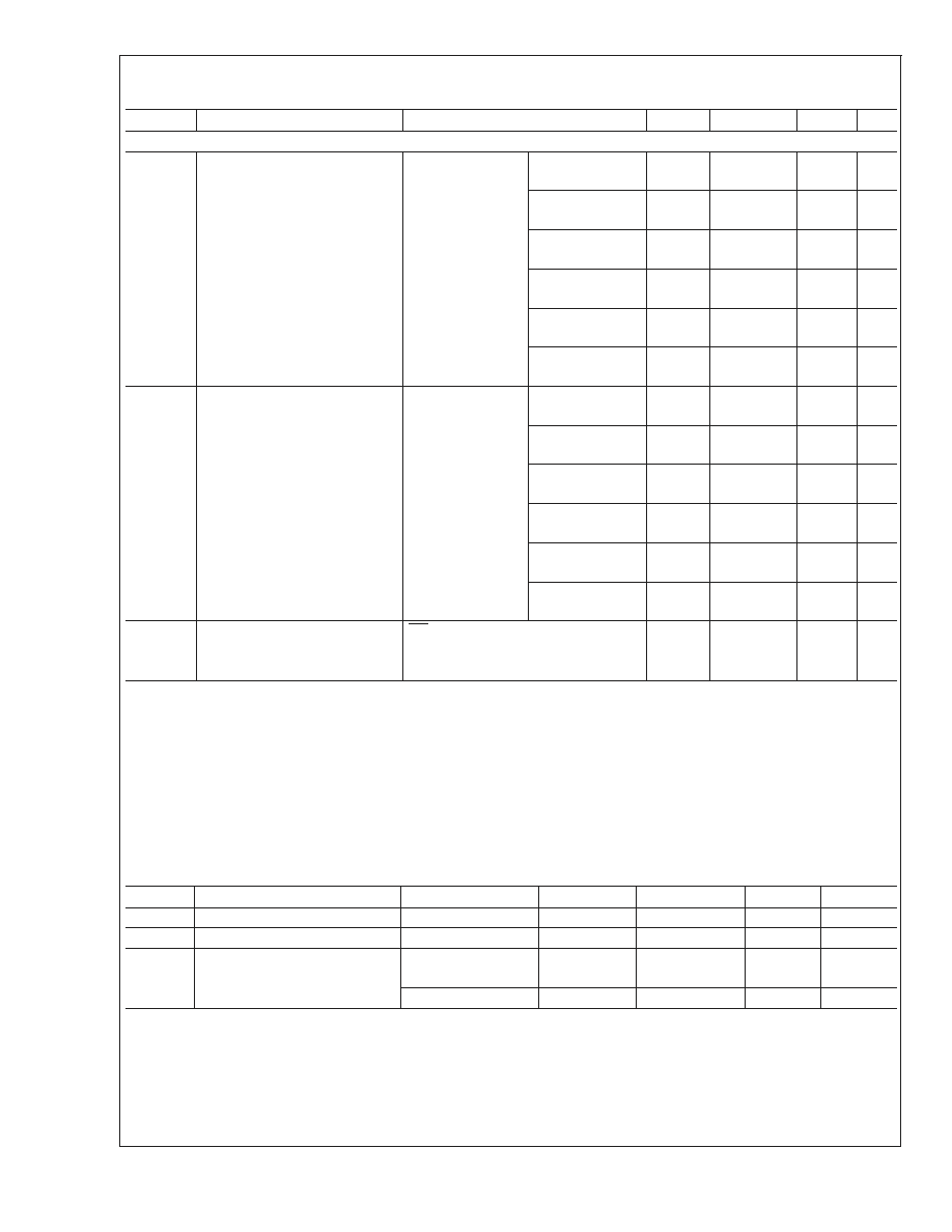
Electrical Characteristics
(Continued)
Over recommended operating supply and temperature ranges unless otherwise specified.(Note 2)
Symbol
Parameter
Conditions
Min
Typ
Max
Units
TRANSMITTER SUPPLY CURRENT
ICCTW
Transmitter Supply Current
Worst Case
R
L
= 100
, C
L
= 5
pF,
Worst Case
Pattern
(Figure 3
, BAL=High
(enabled), V
CC
=
3.6V
f = 32.5 MHz,
DUAL = V
CC
115
180
mA
f = 32.5 MHz,
DUAL = Gnd
75
mA
f = 65 MHz,
DUAL = V
CC
150
215
mA
f = 65 MHz,
DUAL = Gnd
95
mA
f = 85 MHz,
DUAL = V
CC
175
235
mA
f = 85 MHz,
DUAL = Gnd
110
mA
ICCTG
Transmitter Supply Current
16 Grayscale Case
R
L
= 100
, C
L
= 5
pF,
16 Grayscale
Pattern
Figure 2, BAL =
High (enabled),
V
CC
= 3.6V
f = 32.5 MHz,
DUAL = V
CC
110
170
mA
f = 32.5 MHz,
DUAL = Gnd
70
mA
f = 65 MHz,
DUAL = V
CC
135
205
mA
f = 65 MHz,
DUAL = Gnd
90
mA
f = 85 MHz,
DUAL = V
CC
155
225
mA
f = 85 MHz,
DUAL = Gnd
100
mA
ICCTZ
Transmitter Supply Current
Power Down
PD = Low
4.8
85
�A
Driver Outputs in TRI-STATE under
Powerdown Mode
Note 1: "Absolute Maximum Ratings" are those values beyond which the safety of the device cannot be guaranteed. They are not meant to imply that the device
should be operated at these limits. The tables of "Electrical Characteristics" specify conditions for device operation.
Note 2: Typical values are given for V
CC
= 3.3V and T
A
= +25�C. Device tested in Non-Balanced mode only.
Note 3: Current into device pins is defined as positive. Current out of device pins is defined as negative. Voltages are referenced to ground unless otherwise
specified (except V
OD
and
V
OD
).
Note 4: Low Swing DC threshold testing is preformed on data and control inputs only. Clock inputs tested by functional testing only.
DIGITAL DC CHARACTERISTICS for Two-Wire Serial Communication
Interface
Over recommended operating supply and temperature ranges unless otherwise specified.(Note 2) Parameters list below only
valid when I2CSEL pin = Vcc.
Symbol
Parameter
Conditions
Min
Typ
Max
Units
V
IN
(1)
Logical " 1 " input voltage
2.1
V
V
IN
(0)
Logical " 0 " input voltage
0.8
V
V
OL
Serial Bus Low level output
voltage
I
OL
=3mA
0.4
V
I
OL
=6mA
0.6
V
DS90C387R
www.national.com
4
Recommended Transmitter Input Characteristics
Over recommended operating supply and temperature ranges unless otherwise specified. Device driving the transmitter inputs
should comply to this table of recommendations.
Symbol
Parameter
Min
Typ
Max
Units
TCIT
TxCLK IN Transition Time (Figure 5)
DUAL = Gnd or V
CC
0.8
1.2
2.4
ns
TCIP
TxCLK IN Period (Figure 6)
DUAL = Gnd or V
CC
11.76
T
40
ns
TCIH
TxCLK in High Time (Figure 6)
0.4T
0.5T
0.6T
ns
TCIL
TxCLK in Low Time (Figure 6)
0.4T
0.5T
0.6T
ns
VDDQ
Low Swing Voltage Amplitude from GMCH
1.0
1.8
V
Transmitter Switching Characteristics
Over recommended operating supply and temperature ranges unless otherwise specified.(Note 2)
Symbol
Parameter
Min
Typ
Max
Units
LLHT
LVDS Low-to-High Transition Time (Figure 4), PRE = no connect
(minimum pre-empahsis).
0.14
0.9
ns
LVDS Low-to-High Transition Time (Figure 4), PRE = V
CC
(max.
pre-empahsis).
0.11
0.7
ns
LHLT
LVDS High-to-Low Transition Time (Figure 4), PRE = no connect
(mini. pre-empahsis).
0.16
0.9
ns
LVDS High-to-Low Transition Time (Figure 4), PRE = V
CC
(max.
pre-empahsis).
0.11
0.7
ns
TCCS
TxOUT Channel to Channel Skew
100
ps
TPPOS0
Transmitter Output Pulse Position for Bit0
from TxCLKout rising edge.
f = 85MHz (Note 8)
-300
0
+300
ps
TPPOS1
Transmitter Output Pulse Position for Bit1
from TxCLKout rising edge.
1.38
1.68
1.98
ns
TPPOS2
Transmitter Output Pulse Position for Bit2
from TxCLKout rising edge.
3.06
3.36
3.66
ns
TPPOS3
Transmitter Output Pulse Position for Bit3
from TxCLKout rising edge.
4.74
5.04
5.34
ns
TPPOS4
Transmitter Output Pulse Position for Bit4
from TxCLKout rising edge.
6.42
6.72
7.02
ns
TPPOS5
Transmitter Output Pulse Position for Bit5
from TxCLKout rising edge.
8.10
8.40
8.70
ns
TPPOS6
Transmitter Output Pulse Position for Bit6
from TxCLKout rising edge.
9.78
10.08
10.38
ns
TSTC
TxIN Setup to TxCLK IN in low swing mode at 85 MHz (Figure 7)
1.8
ns
THTC
TxIN Hold to TxCLK IN in low swing mode at 85 MHz (Figure 7)
2
ns
TJCC
Transmitter Jitter Cycle-to-cycle (Figures
12, 13) (Note 5), DUAL = Gnd, V
CC
= 3V
f = 85 MHz
110
150
ps
f = 65 MHz
80
120
ps
f = 32.5 MHz
75
115
ps
TPLLS
Transmitter Phase Lock Loop Set (Figure 8)
10
ms
TPDD
Transmitter Powerdown Delay (Figure 9)
100
ns
TPDL
Transmitter Input to Output Latency (Figure
10)
f = 32.5/65/85 MHz
(Note 9)
1.5TCIP
+4.1
ns
DS90C387R
www.national.com
5