 | –≠–ª–µ–∫—Ç—Ä–æ–Ω–Ω—ã–π –∫–æ–º–ø–æ–Ω–µ–Ω—Ç: DS90CF581 | –°–∫–∞—á–∞—Ç—å:  PDF PDF  ZIP ZIP |
DS90CF581
LVDS Transmitter 24-Bit Color Flat Panel Display (FPD)
Link
General Description
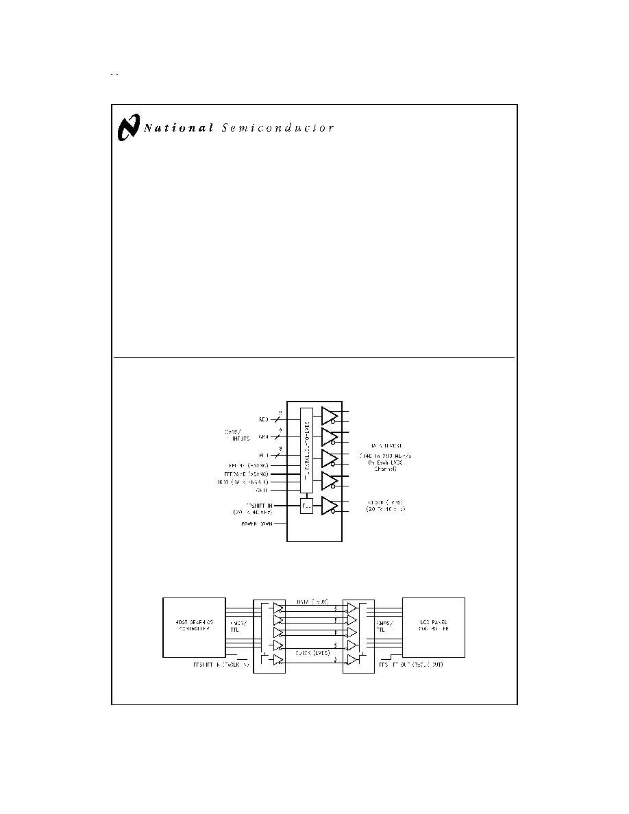
The DS90CF581 transmitter converts 28 bits of CMOS/TTL
data into four LVDS (Low Voltage Differential Signaling) data
streams. A phase-locked transmit clock is transmitted in par-
allel with the data streams over a fifth LVDS link. Every cycle
of the transmit clock 28 bits of input data are sampled and
transmitted. At a transmit clock frequency of 40 MHz, 24 bits
of RGB data and 4 bits of LCD timing and control data
(FPLINE, FPFRAME, DRDY, CNTL) are transmitted at a rate
of 280 Mbps per LVDS data channel. Using a 40 MHz clock,
the data throughput is 140 Megabytes per second. This
transmitter is intended to interface to any of the FPD Link re-
ceivers.
The chipset is an ideal means to solve EMI and cable size
problems associated with wide, high speed TTL interfaces.
Features
n
Up to 140 Megabyte/sec Bandwidth
n
Narrow bus reduces cable size and cost
n
290 mV swing LVDS devices for low EMI
n
Low power CMOS design
n
Power-down mode
n
PLL requires no external components
n
Low profile 56-lead TSSOP package
n
Falling edge data strobe
n
Compatible with TIA/EIA-644 LVDS standard
Block Diagrams
TRI-STATE
Æ
is a registered trademark of National Semiconductor Corporation.
DS90CF581
DS012486-28
Order Number DS90CF581MTD
See NS Package Number MTD56
Application
DS012486-2
June 1998
DS90CF581
L
VDS
T
ransmitter
24-Bit
Color
Flat
Panel
Display
(FPD)
Link
© 1998 National Semiconductor Corporation
DS012486
www.national.com
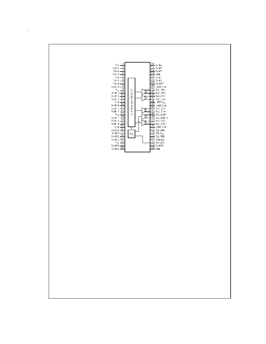
Connection Diagram
DS90CF581
DS012486-3
www.national.com
2
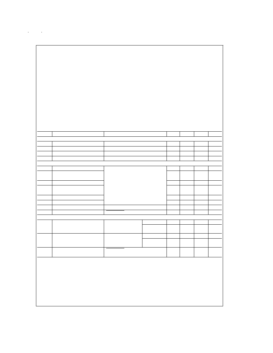
Absolute Maximum Ratings
(Note 1)
If Military/Aerospace specified devices are required,
please contact the National Semiconductor Sales Office/
Distributors for availability and specifications.
Supply Voltage (V
CC
)
-0.3 to +6V
CMOS/TTL Input Voltage
-0.3 to (V
CC
+ 0.3V)
LVDS Driver Output Voltage
-0.3 to (V
CC
+ 0.3V)
LVDS Output Short Circuit
Duration
continuous
Junction Temperature
+150∞C
Storage Temperature Range
-65∞C to +150∞C
Lead Temperature
(Soldering, 4 sec.)
+260∞C
Maximum Package Power Dissipation
@
+25∞C
MTD56 (TSSOP) Package:
DS90CF581
1.63W
Derate Package:
DS90CF581
12.5 mW/∞C above
+25∞C
This device does not meet 2000V ESD rating. (Note 4)
Recommended Operating
Conditions
Min
Nom
Max
Units
Supply Voltage (V
CC
)
4.5
5.0
5.5
V
Operating Free
Air Temperature (T
A
)
-10
+25
+70
∞C
Receiver Input Range
0
2.4
V
Supply Noise Voltage (V
CC
)
100
mV
P-P
Electrical Characteristics
Over recommended operating supply and temperature ranges unless otherwise specified
Symbol
Parameter
Conditions
Min
Typ
Max
Units
CMOS/TTL DC SPECIFICATIONS
V
IH
High Level Input Voltage
2.0
V
CC
V
V
IL
Low Level Input Voltage
GND
0.8
V
V
CL
Input Clamp Voltage
I
CL
= -18 mA
-0.79
-1.5
V
I
IN
Input Current
V
IN
= V
CC
, GND, 2.5V or 0.4V
±
5.1
±
10
µA
LVDS DRIVER DC SPECIFICATIONS
V
OD
Differential Output Voltage
R
L
= 100
250
290
450
mV
V
OD
Change in V
OD
between
35
mV
Complimentary Output States
V
OS
Offset Voltage (Note 5)
1.1
1.25
1.375
V
V
OS
Change in V
OS
between
35
mV
Complimentary Output States
V
OH
High Level Output Voltage
1.3
1.6
V
V
OL
Low Level Output Voltage
0.9
1.01
V
I
OS
Output Short Circuit Current
V
OUT
= 0V, R
L
= 100
-2.9
-5
mA
I
OZ
Output TRI-STATE
Æ
Current
Power Down = 0V, V
OUT
= 0V or V
CC
±
1
±
10
µA
TRANSMITTER SUPPLY CURRENT
I
CCTW
Transmitter Supply Current,
R
L
= 100
, C
L
= 5 pF,
f = 32.5 MHz
34
51
mA
Worst Case
Worst Case Pattern
(
Figure 1, Figure 3)
f = 37.5 MHz
36
53
mA
I
CCTG
Transmitter Supply Current,
R
L
= 100
, C
L
= 5 pF,
f = 32.5 MHz
27
47
mA
16 Grayscale
Grayscale Pattern
(
Figure 2, Figure 3)
f = 37.5 MHz
28
48
mA
I
CCTZ
Transmitter Supply Current,
Power Down = Low
1
25
µA
Power Down
Note 1: "Absolute Maximum Ratings" are those values beyond which the safety of the device cannot be guaranteed. They are not meant to imply that the device
should be operated at these limits. The tables of "Electrical Characteristics" specify conditions for device operation.
Note 2: Typical values are given for V
CC
= 5.0V and T
A
= +25∞C.
Note 3: Current into device pins is defined as positive. Current out of device pins is defined as negative. Voltages are referenced to ground unless otherwise speci-
fied (except V
OD
and
V
OD
).
Note 4: ESD Rating: HBM (1.5 k
, 100 pF)
PLL V
CC
1000V
All other pins
2000V
EIAJ (0
, 200 pF)
150V
Note 5: V
OS
previously referred as V
CM
.
www.national.com
3
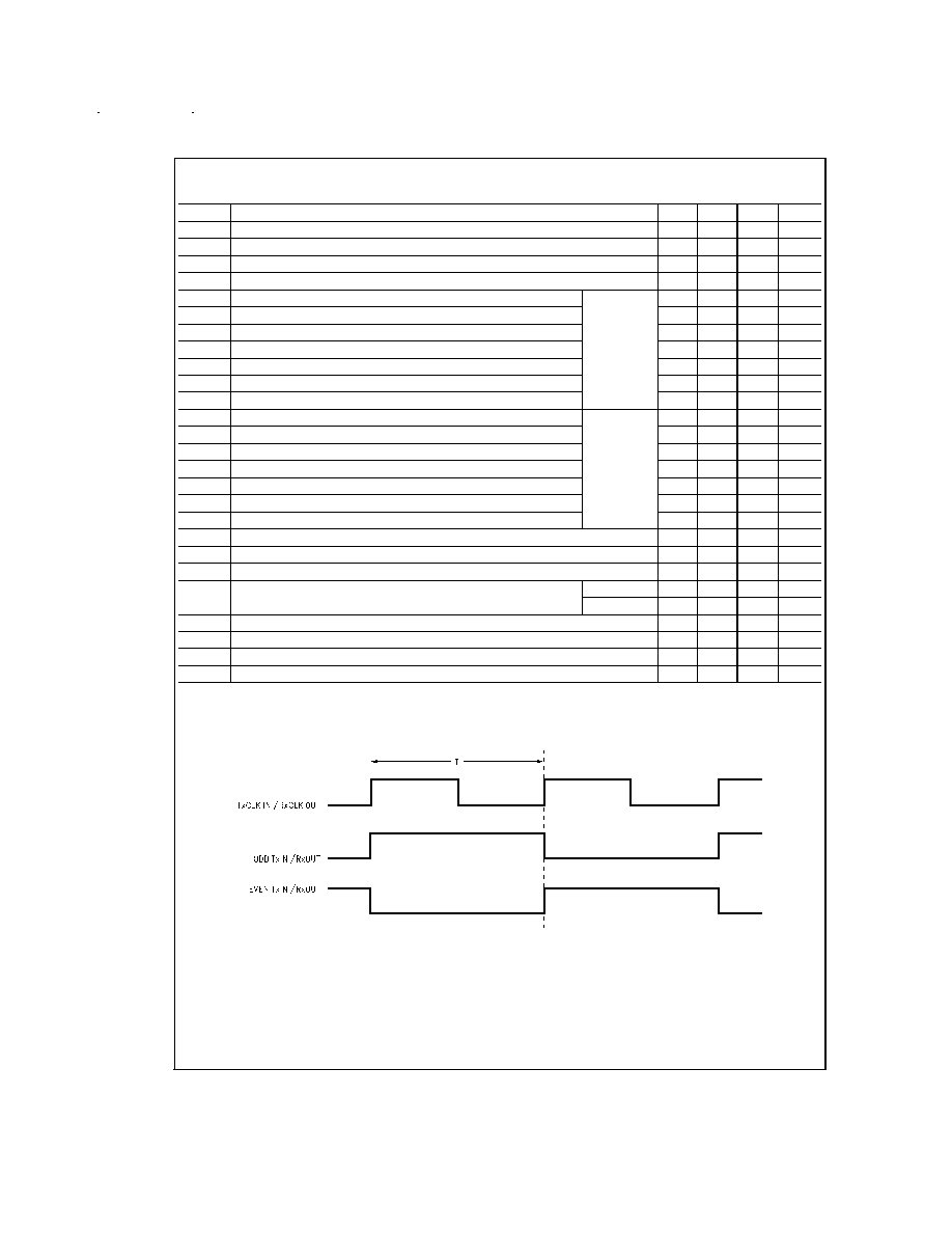
Transmitter Switching Characteristics
Over recommended operating supply and temperature ranges unless otherwise specified
Symbol
Parameter
Min
Typ
Max
Units
LLHT
LVDS Low-to-High Transition Time (
Figure 3)
0.75
1.5
ns
LHLT
LVDS High-to-Low Transition Time (
Figure 3)
0.75
1.5
ns
TCIT
TxCLK IN Transition Time (
Figure 4)
8
ns
TCCS
TxOUT Channel-to-Channel Skew (Note 6) (
Figure 5)
350
ps
TPPos0
Transmitter Output Pulse Position for Bit 0 (
Figure 11)
f = 20 MHz
-200
150
350
ps
TPPos1
Transmitter Output Pulse Position for Bit 1
6.3
7.2
7.5
ns
TPPos2
Transmitter Output Pulse Position for Bit 2
12.8
13.6
14.6
ns
TPPos3
Transmitter Output Pulse Position for Bit 3
20
20.8
21.5
ns
TPPos4
Transmitter Output Pulse Position for Bit 4
27.2
28
28.5
ns
TPPos5
Transmitter Output Pulse Position for Bit 5
34.5
35.2
35.6
ns
TPPos6
Transmitter Output Pulse Position for Bit 6
42.2
42.6
42.9
ns
TPPos0
Transmitter Output Pulse Position for Bit 0 (
Figure 11)
f = 40 MHz
-100
100
300
ps
TPPos1
Transmitter Output Pulse Position for Bit 1
2.9
3.3
3.9
ns
TPPos2
Transmitter Output Pulse Position for Bit 2
6.1
6.6
7.1
ns
TPPos3
Transmitter Output Pulse Position for Bit 3
9.7
10.2
10.7
ns
TPPos4
Transmitter Output Pulse Position for Bit 4
13
13.5
14.1
ns
TPPos5
Transmitter Output Pulse Position for Bit 5
17
17.4
17.8
ns
TPPos6
Transmitter Output Pulse Position for Bit 6
20.3
20.8
21.4
ns
TCIP
TxCLK IN Period (
Figure 6)
25
T
50
ns
TCIH
TxCLK IN High Time (
Figure 6)
0.35T
0.5T
0.65T
ns
TCIL
TxCLK IN Low Time (
Figure 6)
0.35T
0.5T
0.65T
ns
TSTC
TxIN Setup to TxCLK IN (
Figure 6)
f = 20 MHz
14
ns
f = 40 MHz
8
ns
THTC
TxIN Hold to TxCLK IN (
Figure 6)
2.5
2
ns
TCCD
TxCLK IN to TxCLK OUT Delay
@
25∞C, V
CC
= 5.0V (Figure 7)
5
9.7
ns
TPLLS
Transmitter Phase Lock Loop Set (
Figure 8)
10
ms
TPDD
Transmitter Powerdown Delay (
Figure 10)
100
ns
Note 6: This limit based on bench characterization.
AC Timing Diagrams
DS012486-15
FIGURE 1. "WORST CASE" Test Pattern
www.national.com
4

AC Timing Diagrams
(Continued)
DS012486-16
Note 7: The worst case test pattern produces a maximum toggling of digital circuits, LVDS I/O and CMOS/TTL I/O.
Note 8: The 16 grayscale test pattern tests device power consumption for a "typical" LCD display pattern. The test pattern approximates signal switching needed
to produce groups of 16 vertical stripes across the display.
Note 9:
Figure 1 and Figure 2 show a falling edge data strobe (TxCLK IN/RxCLK OUT).
Note 10: Recommended pin to signal mapping. Customer may choose to define differently.
FIGURE 2. "16 GRAYSCALE" Test Pattern (Notes 7, 8, 9, 10)
DS012486-8
DS012486-9
FIGURE 3. DS90CF581 (Transmitter) LVDS Output Load and Transition Timing
www.national.com
5