 | –≠–ª–µ–∫—Ç—Ä–æ–Ω–Ω—ã–π –∫–æ–º–ø–æ–Ω–µ–Ω—Ç: DS90CR216 | –°–∫–∞—á–∞—Ç—å:  PDF PDF  ZIP ZIP |

DS90CR215/DS90CR216
+3.3V Rising Edge Data Strobe LVDS 21-Bit Channel
Link - 66 MHz
General Description
The DS90CR215 transmitter converts 21 bits of CMOS/TTL
data into three LVDS (Low Voltage Differential Signaling)
data streams. A phase-locked transmit clock is transmitted in
parallel with the data streams over a fourth LVDS link. Every
cycle of the transmit clock 21 bits of input data are sampled
and transmitted. The DS90CR216 receiver converts the
LVDS data streams back into 21 bits of CMOS/TTL data. At
a transmit clock frequency of 66 MHz, 21 bits of TTL data are
transmitted at a rate of 462 Mbps per LVDS data channel.
Using a 66 MHz clock, the data throughput is 1.386 Gbit/s
(173 Mbytes/s).
The multiplexing of the data lines provides a substantial
cable reduction. Long distance parallel single-ended buses
typically require a ground wire per active signal (and have
very limited noise rejection capability). Thus, for a 21-bit wide
data and one clock, up to 44 conductors are required. With
the Channel Link chipset as few as 9 conductors (3 data
pairs, 1 clock pair and a minimum of one ground) are
needed. This provides a 80% reduction in required cable
width, which provides a system cost savings, reduces con-
nector physical size and cost, and reduces shielding require-
ments due to the cables' smaller form factor.
The 21 CMOS/TTL inputs can support a variety of signal
combinations. For example, five 4-bit nibbles plus 1 control,
or two 9-bit (byte + parity) and 3 control.
Features
n
Single +3.3V supply
n
Chipset (Tx + Rx) power consumption
<
250 mW (typ)
n
Power-down mode (
<
0.5 mW total)
n
Up to 173 Megabytes/sec bandwidth
n
Up to 1.386 Gbps data throughput
n
Narrow bus reduces cable size
n
290 mV swing LVDS devices for low EMI
n
+1V common mode range (around +1.2V)
n
PLL requires no external components
n
Low profile 48-lead TSSOP package
n
Rising edge data strobe
n
Compatible with TIA/EIA-644 LVDS standard
n
ESD Rating
>
7 kV
n
Operating Temperature: -40∞C to +85∞C
Block Diagrams
TRI-STATE
Æ
is a registered trademark of National Semiconductor Corporation.
DS90CR215
DS012909-1
Order Number DS90CR215MTD
See NS Package Number MTD48
DS90CR216
DS012909-27
Order Number DS90CR216MTD
See NS Package Number MTD48
March 1999
DS90CR215/DS90CR216
+3.3V
Rising
Edge
Data
Strobe
L
VDS
21-Bit
Channel
Link-66
MHz
© 1999 National Semiconductor Corporation
DS012909
www.national.com
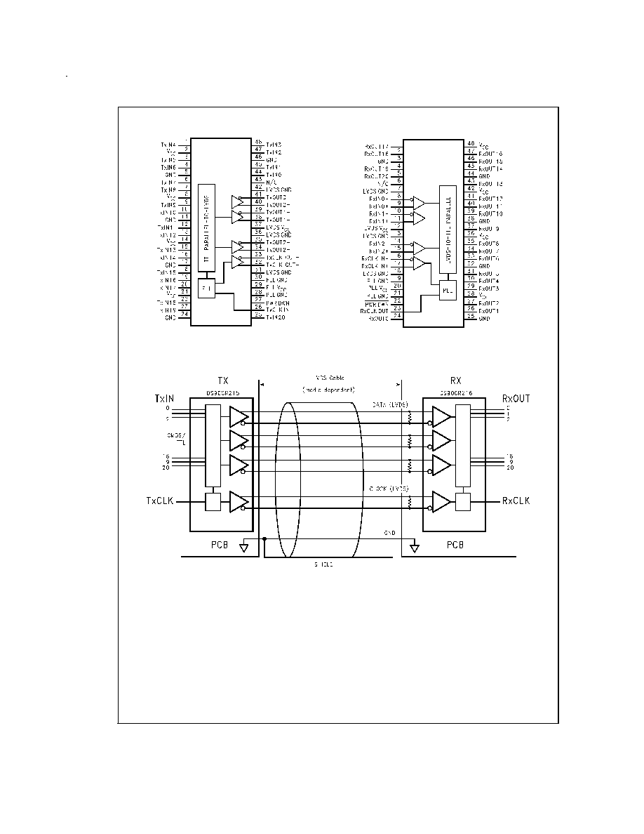
Pin Diagrams
Typical Application
DS012909-21
DS90CR215
DS012909-22
DS90CR216
DS012909-23
www.national.com
2
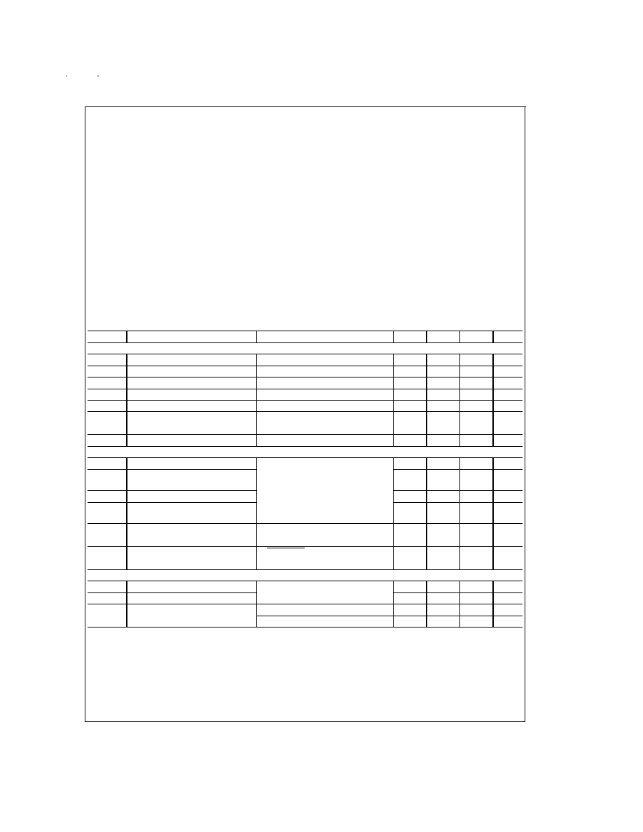
Absolute Maximum Ratings
(Note 1)
If Military/Aerospace specified devices are required,
please contact the National Semiconductor Sales Office/
Distributors for availability and specifications.
Supply Voltage (V
CC
)
-0.3V to +4V
CMOS/TTL Input Voltage
-0.3V to (V
CC
+ 0.3V)
CMOS/TTL Output Voltage
-0.3V to (V
CC
+ 0.3V)
LVDS Receiver Input Voltage
-0.3V to (V
CC
+ 0.3V)
LVDS Driver Output Voltage
-0.3V to (V
CC
+ 0.3V)
LVDS Output Short
Circuit Duration
Continuous
Junction Temperature
+150∞C
Storage Temperature Range
-65∞C to +150∞C
Lead Temperature
(Soldering, 4 sec.)
+260∞C
Maximum Package Power Dissipation
@
+25∞C
MTD48 (TSSOP) Package:
DS90CR215
1.98 W
DS90CR216
1.89 W
Package Derating
DS90CR215
16 mW/∞C above +25∞C
DS90CR216
15 mW/∞C above +25∞C
ESD Rating
(HBM, 1.5 k
, 100 pF)
>
7 kV
Recommended Operating
Conditions
Min
Nom
Max
Units
Supply Voltage (V
CC
)
3.0
3.3
3.6
V
Operating Free Air
Temperature (T
A
)
-40
+25
+85
∞C
Receiver Input Range
0
2.4
V
Supply Noise Voltage (V
CC
)
100 mV
PP
Electrical Characteristics
Over recommended operating supply and temperature ranges unless otherwise specified
Symbol
Parameter
Conditions
Min
Typ
Max
Units
CMOS/TTL DC SPECIFICATIONS
V
IH
High Level Input Voltage
2.0
V
CC
V
V
IL
Low Level Input Voltage
GND
0.8
V
V
OH
High Level Output Voltage
I
OH
= -0.4 mA
2.7
3.3
V
V
OL
Low Level Output Voltage
I
OL
= 2 mA
0.06
0.3
V
V
CL
Input Clamp Voltage
I
CL
= -18 mA
-0.79
-1.5
V
I
IN
Input Current
V
IN
= V
CC
, GND,
±
5.1
±
10
µA
2.5V or 0.4V
I
OS
Output Short Circuit Current
V
OUT
= 0V
-60
-120
mA
LVDS DRIVER DC SPECIFICATIONS
V
OD
Differential Output Voltage
R
L
= 100
250
290
450
mV
V
OD
Change in V
OD
between
Complimentary Output States
35
mV
V
OS
Offset Voltage (Note 4)
1.125
1.25
1.375
V
V
OS
Change in V
OS
between
Complimentary Output States
35
mV
I
OS
Output Short Circuit Current
V
OUT
= 0V,
-3.5
-5
mA
R
L
= 100
I
OZ
Output TRI-STATE
Æ
Current
PWR DWN = 0V,
±
1
±
10
µA
V
OUT
= 0V or V
CC
LVDS RECEIVER DC SPECIFICATIONS
V
TH
Differential Input High Threshold
V
CM
= +1.2V
+100
mV
V
TL
Differential Input Low Threshold
-100
mV
I
IN
Input Current
V
IN
= +2.4V, V
CC
= 3.6V
±
10
µA
V
IN
= 0V, V
CC
= 3.6V
±
10
µA
www.national.com
3
Electrical Characteristics
(Continued)
Over recommended operating supply and temperature ranges unless otherwise specified
Symbol
Parameter
Conditions
Min
Typ
Max
Units
TRANSMITTER SUPPLY CURRENT
I
CCTW
Transmitter Supply Current
Worst Case (with Loads)
R
L
= 100
,
C
L
= 5 pF,
Worst Case
Pattern
(
Figures 1, 2),
T
A
= -10∞C to
+70∞C
f = 32.5 MHz
31
45
mA
f = 37.5 MHz
32
50
mA
f = 66 MHz
37
55
mA
R
L
= 100
,
C
L
= 5 pF,
Worst Case
Pattern
(
Figures 1, 2),
T
A
= -40∞C to
+85∞C
f = 40 MHz
38
51
mA
f = 66 MHz
42
55
mA
I
CCTZ
Transmitter Supply Current
Power Down
PWR DWN = Low
Driver Outputs in TRI-STATE
under Powerdown Mode
10
55
µA
RECEIVER SUPPLY CURRENT
I
CCRW
Receiver Supply Current Worst
Case
C
L
= 8 pF,
Worst Case
Pattern
(
Figures 1, 3),
T
A
= -10∞C to
+70∞C
f = 32.5 MHz
49
65
mA
f = 37.5 MHz
53
70
mA
f = 66 MHz
78
105
mA
C
L
= 8 pF,
Worst Case
Pattern
(
Figures 1, 3),
T
A
= -40∞C to
+85∞C
f = 40 MHz
55
82
mA
f = 66 MHz
78
105
mA
I
CCRZ
Receiver Supply Current Power
Down
PWR DWN = Low
Receiver Outputs Stay Low during
Powerdown Mode
10
55
µA
Note 1: "Absolute Maximum Ratings" are those values beyond which the safety of the device cannot be guaranteed. They are not meant to imply that the device
should be operated at these limits. The tables of "Electrical Characteristics" specify conditions for device operation.
Note 2: Typical values are given for V
CC
= 3.3V and T
A
= +25∞C.
Note 3: Current into device pins is defined as positive. Current out of device pins is defined as negative. Voltages are referenced to ground unless otherwise speci-
fied (except V
OD
and
V
OD
).
Note 4: V
OS
previously referred as V
CM
.
Transmitter Switching Characteristics
Over recommended operating supply and -40∞C to +85∞C ranges unless otherwise specified
Symbol
Parameter
Min
Typ
Max
Units
LLHT
LVDS Low-to-High Transition Time (
Figure 2)
0.5
1.5
ns
LHLT
LVDS High-to-Low Transition Time (
Figure 2)
0.5
1.5
ns
TCIT
TxCLK IN Transition Time (
Figure 4)
5
ns
TCCS
TxOUT Channel-to-Channel Skew (
Figure 5)
250
ps
TPPos0
Transmitter Output Pulse Position for
Bit0 (Note 7) (
Figure 16)
f = 40 MHz
-0.4
0
0.4
ns
TPPos1
Transmitter Output Pulse Position for
Bit1
3.1
3.3
4.0
ns
TPPos2
Transmitter Output Pulse Position for
Bit2
6.5
6.8
7.6
ns
www.national.com
4
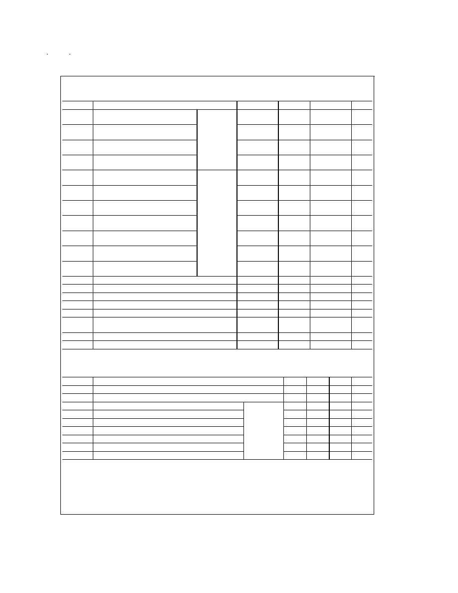
Transmitter Switching Characteristics
(Continued)
Over recommended operating supply and -40∞C to +85∞C ranges unless otherwise specified
Symbol
Parameter
Min
Typ
Max
Units
TPPos3
Transmitter Output Pulse Position for
Bit3
10.2
10.4
11.0
ns
TPPos4
Transmitter Output Pulse Position for
Bit4
13.7
13.9
14.6
ns
TPPos5
Transmitter Output Pulse Position for
Bit5
17.3
17.6
18.2
ns
TPPos6
Transmitter Output Pulse Position for
Bit6
21.0
21.2
21.8
ns
TPPos0
Transmitter Output Pulse Position for
Bit0 (Note 6) (
Figure 16)
f = 66 MHz
-0.4
0
0.3
ns
TPPos1
Transmitter Output Pulse Position for
Bit1
1.8
2.2
2.5
ns
TPPos2
Transmitter Output Pulse Position for
Bit2
4.0
4.4
4.7
ns
TPPos3
Transmitter Output Pulse Position for
Bit3
6.2
6.6
6.9
ns
TPPos4
Transmitter Output Pulse Position for
Bit4
8.4
8.8
9.1
ns
TPPos5
Transmitter Output Pulse Position for
Bit5
10.6
11.0
11.3
ns
TPPos6
Transmitter Output Pulse Position for
Bit6
12.8
13.2
13.5
ns
TCIP
TxCLK IN Period (
Figure 6)
15
T
50
ns
TCIH
TxCLK IN High Time (
Figure 6)
0.35T
0.5T
0.65T
ns
TCIL
TxCLK IN Low Time (
Figure 6)
0.35T
0.5T
0.65T
ns
TSTC
TxIN Setup to TxCLK IN (
Figure 6)
2.5
ns
THTC
TxIN Hold to TxCLK IN (
Figure 6)
0
ns
TCCD
TxCLK IN to TxCLK OUT Delay
@
25∞C,V
CC
=3.3V
(
Figure 8)
3
3.7
5.5
ns
TPLLS
Transmitter Phase Lock Loop Set (
Figure 10)
10
ms
TPDD
Transmitter Powerdown Delay (
Figure 14)
100
ns
Receiver Switching Characteristics
Over recommended operating supply and -40∞C to +85∞C ranges unless otherwise specified
Symbol
Parameter
Min
Typ
Max
Units
CLHT
CMOS/TTL Low-to-High Transition Time (
Figure 3)
2.2
5.0
ns
CHLT
CMOS/TTL High-to-Low Transition Time (
Figure 3)
2.2
5.0
ns
RSPos0
Receiver Input Strobe Position for Bit 0 (Note 7)(
Figure 17)
f = 40 MHz
1.0
1.4
2.15
ns
RSPos1
Receiver Input Strobe Position for Bit 1
4.5
5.0
5.8
ns
RSPos2
Receiver Input Strobe Position for Bit 2
8.1
8.5
9.15
ns
RSPos3
Receiver Input Strobe Position for Bit 3
11.6
11.9
12.6
ns
RSPos4
Receiver Input Strobe Position for Bit 4
15.1
15.6
16.3
ns
RSPos5
Receiver Input Strobe Position for Bit 5
18.8
19.2
19.9
ns
RSPos6
Receiver Input Strobe Position for Bit 6
22.5
22.9
23.6
ns
www.national.com
5
Receiver Switching Characteristics
(Continued)
Over recommended operating supply and -40∞C to +85∞C ranges unless otherwise specified
Symbol
Parameter
Min
Typ
Max
Units
RSPos0
Receiver Input Strobe Position for Bit 0 (Note 6)(
Figure 17)
f = 66 MHz
0.7
1.1
1.4
ns
RSPos1
Receiver Input Strobe Position for Bit 1
2.9
3.3
3.6
ns
RSPos2
Receiver Input Strobe Position for Bit 2
5.1
5.5
5.8
ns
RSPos3
Receiver Input Strobe Position for Bit 3
7.3
7.7
8.0
ns
RSPos4
Receiver Input Strobe Position for Bit 4
9.5
9.9
10.2
ns
RSPos5
Receiver Input Strobe Position for Bit 5
11.7
12.1
12.4
ns
RSPos6
Receiver Input Strobe Position for Bit 6
13.9
14.3
14.6
ns
RSKM
RxIN Skew Margin (Note 5) (
Figure 18)
f = 40 MHz
490
ps
f = 66 MHz
400
ps
RCOP
RxCLK OUT Period (
Figure 7)
15
T
50
ns
RCOH
RxCLK OUT High Time (
Figure 7)
f = 40 MHz
6.0
10.0
ns
f = 66 MHz
4.0
6.1
ns
RCOL
RxCLK OUT Low Time (
Figure 7)
f = 40 MHz
10.0
13.0
ns
f = 66 MHz
6.0
7.8
ns
RSRC
RxOUT Setup to RxCLK OUT (
Figure 7)
f = 40 MHz
6.5
14.0
ns
f = 66 MHz
2.5
8.0
ns
RHRC
RxOUT Hold to RxCLK OUT (
Figure 7)
f = 40 MHz
6.0
8.0
ns
f = 66 MHz
2.5
4.0
ns
RCCD
RxCLK IN to RxCLK OUT Delay (
Figure 9)
f = 40 MHz
4.0
6.7
8.0
ns
f = 66 MHz
5.0
6.6
9.0
ns
RPLLS
Receiver Phase Lock Loop Set (
Figure 11)
10
ms
RPDD
Receiver Powerdown Delay (
Figure 15)
1
µs
Note 5: Receiver Skew Margin is defined as the valid data sampling region at the receiver inputs. This margin takes into account for transmitter pulse positions (min
and max) and the receiver input setup and hold time (internal data sampling window). This margin allows LVDS interconnect skew, inter-symbol interference (both
dependent on type/length of cable), and clock jitter less than 250 ps.
Note 6: The min. and max. limits are based on the worst bit by applying a -400ps/+300ps shift from ideal position.
Note 7: The min. and max. are based on the actual bit position of each of the 7 bits within the LVDS data stream across PVT.
AC Timing Diagrams
DS012909-2
FIGURE 1. "Worst Case" Test Pattern
DS012909-3
DS012909-4
FIGURE 2. DS90CR215 (Transmitter) LVDS Output Load and Transition Times
www.national.com
6
AC Timing Diagrams
(Continued)
DS012909-5
DS012909-6
FIGURE 3. DS90CR216 (Receiver) CMOS/TTL Output Load and Transition Times
DS012909-7
FIGURE 4. D590CR215 (Transmitter) Input Clock Transition Time
DS012909-8
Note 8: Measurements at V
DIFF
= 0V
Note 9: TCCS measured between earliest and latest LVDS edges
Note 10: TxCLK Differential Low
High Edge
FIGURE 5. D590CR215 (Transmitter) Channel-to-Channel Skew
DS012909-9
FIGURE 6. D590CR215 (Transmitter) Setup/Hold and High/Low Times
www.national.com
7
AC Timing Diagrams
(Continued)
DS012909-10
FIGURE 7. D590CR216 (Receiver) Setup/Hold and High/Low Times
DS012909-11
FIGURE 8. DS90CR215 (Transmitter) Clock In to Clock Out Delay
DS012909-12
FIGURE 9. D590CR216 (Receiver) Clock In to Clock Out Delay
DS012909-13
FIGURE 10. DS90CR215 (Transmitter) Phase Lock Loop Set Time
www.national.com
8

AC Timing Diagrams
(Continued)
DS012909-14
FIGURE 11. DS9OCR216 (Receiver) Phase Lock Loop Set Time
DS012909-15
FIGURE 12. Seven Bits of LVDS in Once Clock Cycle
DS012909-16
FIGURE 13. 21 Parallel TTL Data Inputs Mapped to LVDS Outputs (DS90CR215)
DS012909-17
FIGURE 14. Transmitter Powerdown Delay
www.national.com
9

AC Timing Diagrams
(Continued)
DS012909-18
FIGURE 15. Receiver Powerdown Delay
DS012909-19
FIGURE 16. Transmitter LVDS Output Pulse Position Measurement
www.national.com
10

AC Timing Diagrams
(Continued)
DS012909-28
FIGURE 17. Receiver LVDS Input Strobe Position
www.national.com
11

AC Timing Diagrams
(Continued)
Applications Information
The DS90CR215 and DS90CR216 are backward compatible
with the existing 5V Channel Link transmitter/receiver pair
(DS90CR213, DS90CR214). To upgrade from a 5V to a 3.3V
system the following must be addressed:
1.
Change 5V power supply to 3.3V. Provide this supply to
the V
CC
, LVDS V
CC
and PLL V
CC
.
2.
Transmitter input and control inputs except 3.3V TTL/
CMOS levels. They are not 5V tolerant.
3.
The receiver powerdown feature when enabled wilI lock
receiver output to a logic low. However, the 5V/66 MHz
receiver maintain the outputs in the previous state when
powerdown occurred.
DS90CR215 Pin Description -- Channel Link Transmitter
Pin Name
I/O
No.
Description
TxIN
I
21
TTL level input.
TxOUT+
O
3
Positive LVDS differential data output.
TxOUT-
O
3
Negative LVDS differential data output.
TxCLK IN
I
1
TTL level clock input. The rising edge acts as data strobe. Pin name TxCLK IN.
TxCLK OUT+
O
1
Positive LVDS differential clock output.
TxCLK OUT-
O
1
Negative LVDS differential clock output.
PWR DWN
I
1
TTL level input. Assertion (low input) TRI-STATEs the outputs, ensuring low current at
power down.
V
CC
I
4
Power supply pins for TTL inputs.
GND
I
5
Ground pins for TTL inputs.
PLL V
CC
I
1
Power supply pins for PLL.
PLL GND
I
2
Ground pins for PLL.
LVDS V
CC
I
1
Power supply pin for LVDS outputs.
LVDS GND
I
3
Ground pins for LVDS outputs.
DS90CR216 Pin Description -- Channel Link Receiver
Pin Name
I/O
No.
Description
RxIN+
I
3
Positive LVDS differential data inputs.
RxIN-
I
3
Negative LVDS differential data inputs.
RxOUT
O
21
TTL level data outputs.
RxCLK IN+
I
1
Positive LVDS differential clock input.
RxCLK IN-
I
1
Negative LVDS differential clock input.
RxCLK OUT
O
1
TTL level clock output. The rising edge acts as data strobe. Pin name RxCLK OUT.
DS012909-20
C -- Setup and Hold Time (Internal data sampling window) defined by Rspos (receiver input strobe position) min and max
Tppos -- Transmitter output pulse position (min and max)
RSKM
Cable Skew (type, length) + Source Clock Jitter (cycle to cycle) (Note 11) + ISI (Inter-symbol interference) (Note 12)
Cable Skew -- typicaIIy 10 ps≠40 ps per foot, media dependent
Note 11: Cycle-to-cycle jitter is less than 250 ps
Note 12: ISI is dependent on interconnect length; may be zero
FIGURE 18. Receiver LVDS Input Skew Margin
www.national.com
12
Applications Information
(Continued)
DS90CR216 Pin Description -- Channel Link Receiver
(Continued)
Pin Name
I/O
No.
Description
PWR DWN
I
1
TTL level input. When asserted (low input) the receiver outputs are low.
V
CC
I
4
Power supply pins for TTL outputs.
GND
I
5
Ground pins for TTL outputs.
PLL V
CC
I
1
Power supply for PLL.
PLL GND
1
2
Ground pin for PLL.
LVDS V
CC
I
1
Power supply pin for LVDS inputs.
LVDS GND
I
3
Ground pins for LVDS inputs.
The Channel Link devices are intended to be used in a wide
variety of data transmission applications. Depending upon
the application the interconnecting media may vary. For ex-
ample, for lower data rate (clock rate) and shorter cable
lengths (
<
2m), the media electrical performance is less criti-
cal. For higher speed/long distance applications the media's
performance becomes more critical. Certain cable construc-
tions provide tighter skew (matched electrical length be-
tween the conductors and pairs). Twin-coax for example, has
been demonstrated at distances as great as 5 meters and
with the maximum data transfer of 1.38 Gbit/s. Additional ap-
plications information can be found in the following National
Interface Application Notes:
AN = ####
Topic
AN-1041
Introduction to Channel Link
AN-1035
PCB Design Guidelines for LVDS and
Link Devices
AN-806
Transmission Line Theory
AN-905
Transmission Line Calculations and
Differential Impedance
AN-916
Cable Information
CABLES: A cable interface between the transmitter and re-
ceiver needs to support the differential LVDS pairs. The 21-
bit CHANNEL LINK chipset (DS90CR215/216) requires four
pairs of signal wires and the 28-bit CHANNEL LINK chipset
(DS90CR285/286) requires five pairs of signal wires. The
ideal cable/connector interface would have a constant 100
differential impedance throughout the path. It is also recom-
mended that cable skew remain below 150 ps ( 66 MHz
clock rate) to maintain a sufficient data sampling window at
the receiver.
In addition to the four or five cable pairs that carry data and
clock, it is recommended to provide at least one additional
conductor (or pair) which connects ground between the
transmitter and receiver. This low impedance ground pro-
vides a common mode return path for the two devices. Some
of the more commonly used cable types for point-to-point ap-
plications include flat ribbon, flex, twisted pair and Twin-
Coax. All are available in a variety of configurations and op-
tions. Flat ribbon cable, flex and twisted pair generally
perform well in short point-to-point applications while Twin-
Coax is good for short and long applications. When using rib-
bon cable, it is recommended to place a ground line between
each differential pair to act as a barrier to noise coupling be-
tween adjacent pairs. For Twin-Coax cable applications, it is
recommended to utilize a shield on each cable pair. All ex-
tended point-to-point applications should also employ an
overall shield surrounding all cable pairs regardless of the
cable type. This overall shield results in improved transmis-
sion parameters such as faster attainable speeds, longer
distances between transmitter and receiver and reduced
problems associated with EMS or EMI.
The high-speed transport of LVDS signals has been demon-
strated on several types of cables with excellent results.
However, the best overall performance has been seen when
using Twin-Coax cable. Twin-Coax has very low cable skew
and EMI due to its construction and double shielding. All of
the design considerations discussed here and listed in the
supplemental application notes provide the subsystem com-
munications designer with many useful guidelines. It is rec-
ommended that the designer assess the tradeoffs of each
application thoroughly to arrive at a reliable and economical
cable solution.
BOARD LAYOUT: To obtain the maximum benefit from the
noise and EMI reductions of LVDS, attention should be paid
to the layout of differential lines. Lines of a differential pair
should always be adjacent to eliminate noise interference
from other signals and take full advantage of the noise can-
celing of the differential signals. The board designer should
also try to maintain equal length on signal traces for a given
differential pair. As with any high speed design, the imped-
ance discontinuities should be limited (reduce the numbers
of vias and no 90 degree angles on traces). Any discontinui-
ties which do occur on one signal line should be mirrored in
the other line of the differential pair. Care should be taken to
ensure that the differential trace impedance match the differ-
ential impedance of the selected physical media (this imped-
ance should also match the value of the termination resistor
that is connected across the differential pair at the receiver's
input). Finally, the location of the CHANNEL LINK TxOUT/
RxIN pins should be as close as possible to the board edge
so as to eliminate excessive pcb runs. All of these consider-
ations will limit reflections and crosstalk which adversely ef-
fect high frequency performance and EMI.
UNUSED INPUTS: All unused inputs at the TxIN inputs of
the transmitter must be tied to ground. All unused outputs at
the RxOUT outputs of the receiver must then be left floating.
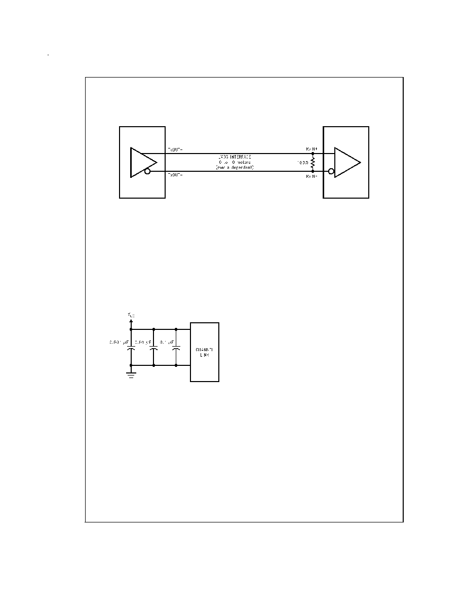
TERMINATION: Use of current mode drivers requires a ter-
minating resistor across the receiver inputs. The CHANNEL
LINK chipset will normally require a single 100
resistor be-
tween the true and complement lines on each differential
pair of the receiver input. The actual value of the termination
resistor should be selected to match the differential mode
characteristic impedance (90
to 120
typical) of the cable.
Figure 19 shows an example. No additional pull-up or pull-
down resistors are necessary as with some other differential
technologies such as PECL. Surface mount resistors are
recommended to avoid the additional inductance that ac-
www.national.com
13
Applications Information
(Continued)
companies leaded resistors. These resistors should be
placed as close as possible to the receiver input pins to re-
duce stubs and effectively terminate the differential lines.
DECOUPLING CAPACITORS: Bypassing capacitors are
needed to reduce the impact of switching noise which could
limit performance. For a conservative approach three
parallel-connected decoupling capacitors (Multi-Layered Ce-
ramic type in surface mount form factor) between each V
CC
and the ground plane(s) are recommended. The three ca-
pacitor values are 0.1 µF, 0.01µF and 0.001 µF. An example
is shown in
Figure 20. The designer should employ wide
traces for power and ground and ensure each capacitor has
its own via to the ground plane. If board space is limiting the
number of bypass capacitors, the PLL V
CC
should receive
the most filtering/bypassing. Next would be the LVDS V
CC
pins and finally the logic V
CC
pins.
CLOCK JITTER: The CHANNEL LINK devices employ a
PLL to generate and recover the clock transmitted across the
LVDS interface. The width of each bit in the serialized LVDS
data stream is one-seventh the clock period. For example, a
66 MHz clock has a period of 15 ns which results in a data bit
width of 2.16 ns. Differential skew (
t within one differential
pair), interconnect skew (
t of one differential pair to an-
other) and clock jitter will all reduce the available window for
sampling the LVDS serial data streams. Care must be taken
to ensure that the clock input to the transmitter be a clean
low noise signal. Individual bypassing of each V
CC
to ground
will minimize the noise passed on to the PLL, thus creating a
low jitter LVDS clock. These measures provide more margin
for channel-to-channel skew and interconnect skew as a part
of the overall jitter/skew budget.
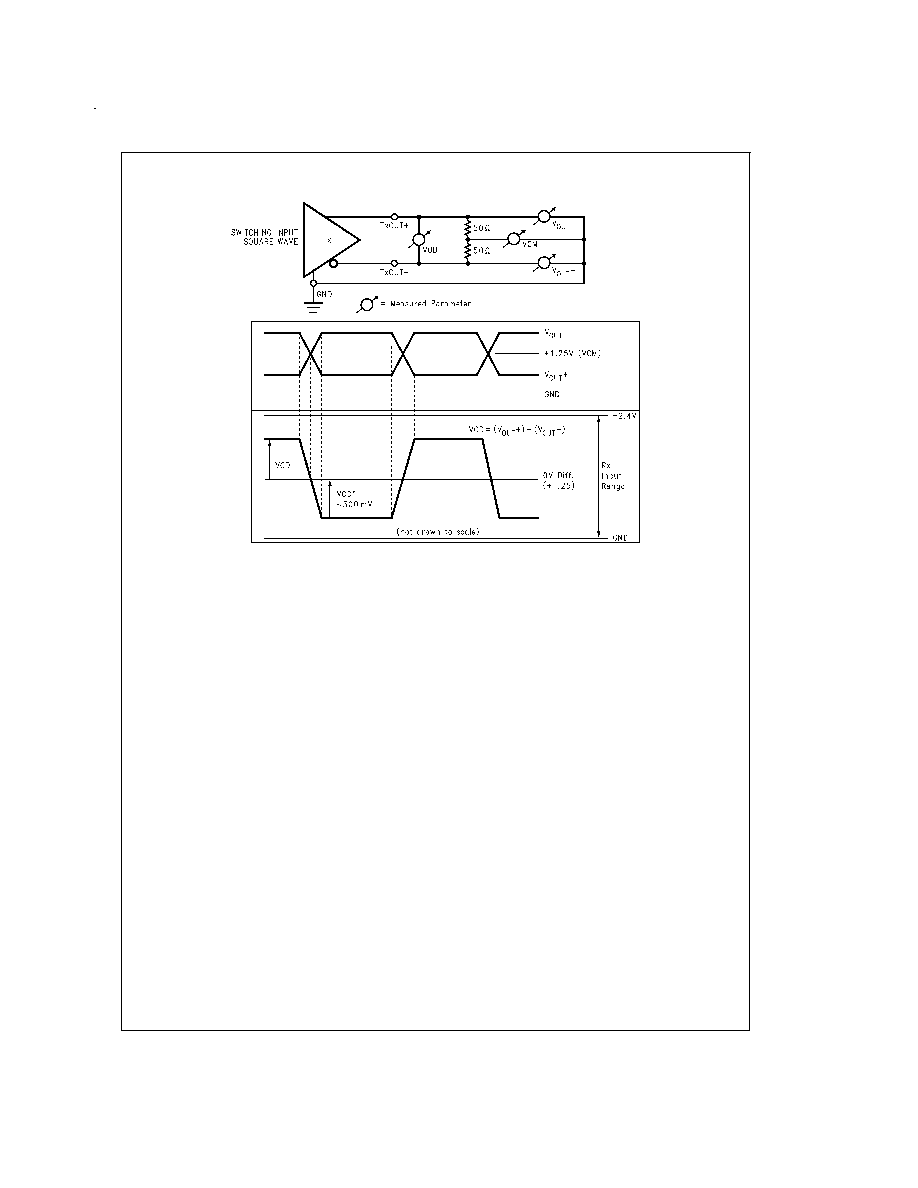
COMMON MODE vs. DIFFERENTIAL MODE NOISE MAR-
GIN: The typical signal swing for LVDS is 300 mV centered
at +1.2V. The CHANNEL LINK receiver supports a 100 mV
threshold therefore providing approximately 200 mV of differ-
ential noise margin. Common mode protection is of more im-
portance to the system's operation due to the differential
data transmission. LVDS supports an input voltage range of
Ground to +2.4V. This allows for a
±
1.0V shifting of the cen-
ter point due to ground potential differences and common
mode noise.
POWER SEQUENCING AND POWERDOWN MODE: Out-
puts of the CNANNEL LINK transmitter remain in TRI-STATE
until the power supply reaches 2V. Clock and data outputs
will begin to toggle 10 ms after V
CC
has reached 3V and the
Powerdown pin is above 1.5V. Either device may be placed
into a powerdown mode at any time by asserting the Power-
down pin (active low). Total power dissipation for each de-
vice will decrease to 5 µW (typical).
The CHANNEL LINK chipset is designed to protect itself
from accidental loss of power to either the transmitter or re-
ceiver. If power to the transmit board is lost, the receiver
clocks (input and output) stop. The data outputs (RxOUT) re-
tain the states they were in when the clocks stopped. When
the receiver board loses power, the receiver inputs are
shorted to V
CC
through an internal diode. Current is limited
(5 mA per input) by the fixed current mode drivers, thus
avoiding the potential for latchup when powering the device.
DS012909-24
FIGURE 19. LVDS Serialized Link Termination
DS012909-25
FIGURE 20. CHANNEL LINK
Decoupling Configuration
www.national.com
14
Applications Information
(Continued)
DS012909-26
FIGURE 21. Single-Ended and Differential Waveforms
www.national.com
15
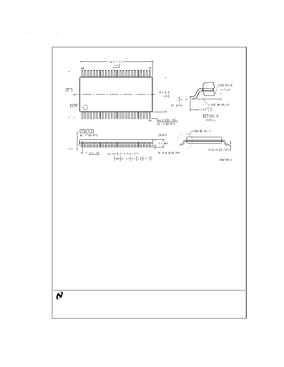
Physical Dimensions
inches (millimeters) unless otherwise noted
LIFE SUPPORT POLICY
NATIONAL'S PRODUCTS ARE NOT AUTHORIZED FOR USE AS CRITICAL COMPONENTS IN LIFE SUPPORT
DEVICES OR SYSTEMS WITHOUT THE EXPRESS WRITTEN APPROVAL OF THE PRESIDENT OF NATIONAL
SEMICONDUCTOR CORPORATION. As used herein:
1. Life support devices or systems are devices or
systems which, (a) are intended for surgical implant
into the body, or (b) support or sustain life, and
whose failure to perform when properly used in
accordance with instructions for use provided in the
labeling, can be reasonably expected to result in a
significant injury to the user.
2. A critical component is any component of a life
support device or system whose failure to perform
can be reasonably expected to cause the failure of
the life support device or system, or to affect its
safety or effectiveness.
National Semiconductor
Corporation
Americas
Tel: 1-800-272-9959
Fax: 1-800-737-7018
Email: support@nsc.com
National Semiconductor
Europe
Fax: +49 (0) 1 80-530 85 86
Email: europe.support@nsc.com
Deutsch Tel: +49 (0) 1 80-530 85 85
English
Tel: +49 (0) 1 80-532 78 32
FranÁais Tel: +49 (0) 1 80-532 93 58
Italiano
Tel: +49 (0) 1 80-534 16 80
National Semiconductor
Asia Pacific Customer
Response Group
Tel: 65-2544466
Fax: 65-2504466
Email: sea.support@nsc.com
National Semiconductor
Japan Ltd.
Tel: 81-3-5639-7560
Fax: 81-3-5639-7507
www.national.com
Order Number DS90CR215MTD or DS90CR216MTD
NS Package Number MTD48
DS90CR215/DS90CR216
+3.3V
Rising
Edge
Data
Strobe
L
VDS
21-Bit
Channel
Link-66
MHz
National does not assume any responsibility for use of any circuitry described, no circuit patent licenses are implied and National reserves the right at any time without notice to change said circuitry and specifications.