 | –≠–ª–µ–∫—Ç—Ä–æ–Ω–Ω—ã–π –∫–æ–º–ø–æ–Ω–µ–Ω—Ç: DS90LV012 | –°–∫–∞—á–∞—Ç—å:  PDF PDF  ZIP ZIP |
DS90LV012A/DS90LT012A
3V LVDS Single CMOS Differential Line Receiver
General Description
The DS90LV012A and DS90LT012A are single CMOS differ-
ential line receivers designed for applications requiring ultra
low power dissipation, low noise, and high data rates. The
devices are designed to support data rates in excess of 400
Mbps (200 MHz) utilizing Low Voltage Differential Swing
(LVDS) technology
The DS90LV012A and DS90LT012A accept low voltage (350
mV typical) differential input signals and translates them to
3V CMOS output levels. The receivers also support open,
shorted, and terminated (100
) input fail-safe. The receiver
output will be HIGH for all fail-safe conditions. The
DS90LV012A has a pinout designed for easy PCB layout.
The DS90LT012A includes an input line termination resistor
for point-to-point applications.
The DS90LV012A and DS90LT012A, and companion LVDS
line driver provide a new alternative to high power PECL/
ECL devices for high speed interface applications.
Features
n
Compatible with ANSI TIA/EIA-644-A Standard
n
>
400 Mbps (200 MHz) switching rates
n
100 ps differential skew (typical)
n
3.5 ns maximum propagation delay
n
Integrated line termination resistor (102
typical)
n
Single 3.3V power supply design (2.7V to 3.6V range)
n
Power down high impedance on LVDS inputs
n
Accepts small swing (350 mV typical) differential signal
levels
n
LVDS receiver inputs accept LVDS/BLVDS/LVPECL
inputs
n
Supports open, short and terminated input fail-safe
n
Pinout simplifies PCB layout
n
Low Power Dissipation (10mW typical
@
3.3V static)
n
SOT-23 5-lead package
n
Leadless LLP-8 package (3x3 mm body size)
n
SOT version pin compatible with SN65LVDS2,
SN65LVDT2
n
Electrically similar to the DS90LV018A
n
Fabricated with advanced CMOS process technology
n
Industrial temperature operating range
(-40∞C to +85∞C)
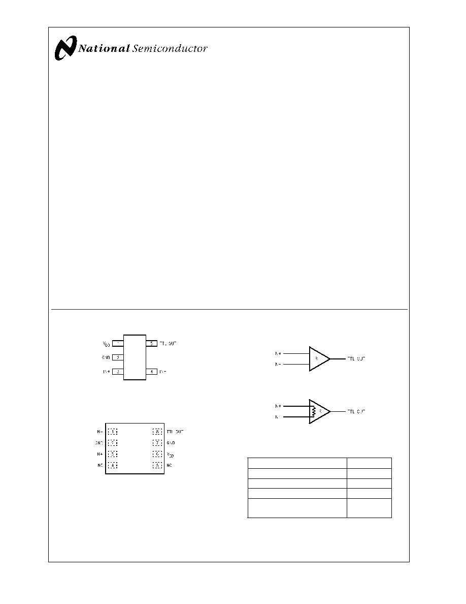
Connection Diagrams
20015026
(Top View)
Order Number DS90LV012ATMF, DS90LT012ATMF
See NS Package Number MF05A
20015027
(Top View)
Order Number DS90LV012ATLD, DS90LT012ATLD
See NS Package Number LDA08A
Functional Diagram
DS90LV012A
20015002
DS90LT012A
20015025
Truth Table
INPUTS
OUTPUT
[IN+] - [IN-]
TTL OUT
V
ID
0V
H
V
ID
-0.1V
L
Full Fail-safe OPEN/SHORT or
Terminated
H
August 2002
DS90L
V012A/DS90L
T012A
3V
L
VDS
Single
CMOS
Differential
Line
Receiver
© 2002 National Semiconductor Corporation
DS200150
www.national.com
Absolute Maximum Ratings
(Note 1)
If Military/Aerospace specified devices are required,
please contact the National Semiconductor Sales Office/
Distributors for availability and specifications.
Supply Voltage (V
DD
)
-0.3V to +4V
Input Voltage (IN+, IN-)
-0.3V to +3.9V
Output Voltage (TTL OUT)
-0.3V to (V
DD
+ 0.3V)
Output Short Circuit Current
-100mA
Maximum Package Power Dissipation
@
+25∞C
LDA Package
2.26 W
Derate LDA Package
18.1 mW/∞C above +25∞C
Thermal resistance (
JA
)
55.3∞C/W
MF Package
902mW
Derate MF Package
7.22 mW/∞C above +25∞C
Thermal resistance (
JA
)
138.5∞C/W
Storage Temperature Range
-65∞C to +150∞C
Lead Temperature Range Soldering
(4 sec.)
+260∞C
Maximum Junction
Temperature
+150∞C
ESD Ratings (Note 4)
Recommended Operating
Conditions
Min
Typ
Max
Units
Supply Voltage (V
DD
)
+2.7
+3.3
+3.6
V
Operating Free Air
Temperature (T
A
)
-40
25
+85
∞C
Electrical Characteristics
Over Supply Voltage and Operating Temperature ranges, unless otherwise specified. (Notes 2, 3)
Symbol
Parameter
Conditions
Pin
Min
Typ
Max
Units
V
TH
Differential Input High Threshold
V
CM
dependant on V
DD
(Note 11)
IN+, IN-
-30
0
mV
V
TL
Differential Input Low Threshold
-100
-30
mV
V
CM
Common-Mode Voltage
V
DD
= 2.7V, V
ID
= 100mV
0.05
2.35
V
V
DD
= 3.0V to 3.6V, V
ID
= 100mV
0.05
V
DD
- 0.3V
V
I
IN
Input Current (DS90LV012A)
V
IN
= +2.8V
V
DD
= 3.6V or 0V
-10
±
1
+10
µA
V
IN
= 0V
-10
±
1
+10
µA
V
IN
= +3.6V
V
DD
= 0V
-20
+20
µA
I
IN
Change in Magnitude of I
IN
V
IN
= +2.8V
V
DD
= 3.6V or 0V
4
µA
V
IN
= 0V
4
µA
V
IN
= +3.6V
V
DD
= 0V
4
µA
I
IND
Differential Input Current
V
IN+
= +0.4V, V
IN-
= +0V
3
3.9
4.4
mA
(DS90LT012A)
V
IN+
= +2.4V, V
IN-
= +2.0V
R
T
Integrated Termination Resistor
(DS90LT012A)
102
C
IN
Input Capacitance
IN+ = IN- = GND
3
pF
V
OH
Output High Voltage
I
OH
= -0.4 mA, V
ID
= +200 mV
TTL OUT
2.4
3.1
V
I
OH
= -0.4 mA, Inputs terminated
2.4
3.1
V
I
OH
= -0.4 mA, Inputs shorted
2.4
3.1
V
V
OL
Output Low Voltage
I
OL
= 2 mA, V
ID
= -200 mV
0.3
0.5
V
I
OS
Output Short Circuit Current
V
OUT
= 0V (Note 5)
-15
-50
-100
mA
V
CL
Input Clamp Voltage
I
CL
= -18 mA
-1.5
-0.7
V
I
DD
No Load Supply Current
Inputs Open
V
DD
5.4
9
mA
DS90L
V012A/DS90L
T012A
www.national.com
2
Switching Characteristics
Over Supply Voltage and Operating Temperature ranges, unless otherwise specified. (Notes 6, 7)
Symbol
Parameter
Conditions
Min
Typ
Max
Units
t
PHLD
Differential Propagation Delay High to Low
C
L
= 15 pF
1.0
1.8
3.5
ns
t
PLHD
Differential Propagation Delay Low to High
V
ID
= 200 mV
1.0
1.7
3.5
ns
t
SKD1
Differential Pulse Skew |t
PHLD
- t
PLHD
| (Note 8)
(Figure 1 and Figure 2)
0
100
400
ps
t
SKD3
Differential Part to Part Skew (Note 9)
0
0.3
1.0
ns
t
SKD4
Differential Part to Part Skew (Note 10)
0
0.4
1.5
ns
t
TLH
Rise Time
350
800
ps
t
THL
Fall Time
175
800
ps
f
MAX
Maximum Operating Frequency (Note 12)
200
250
MHz
Note 1: "Absolute Maximum Ratings" are those values beyond which the safety of the device cannot be guaranteed. They are not meant to imply that the devices
should be operated at these limits. The table of "Electrical Characteristics" specifies conditions of device operation.
Note 2: Current into device pins is defined as positive. Current out of device pins is defined as negative. All voltages are referenced to ground unless otherwise
specified (such as V
ID
).
Note 3: All typicals are given for: V
DD
= +3.3V and T
A
= +25∞C.
Note 4: ESD Ratings:
DS90LV012A:
HBM (1.5 k
, 100 pF) 2kV
EIAJ (0
, 200 pF) 900V
CDM
2000V
IEC direct (330
, 150 pF) 5kV
DS90LT012A:
HBM (1.5 k
, 100 pF) 2kV
EIAJ (0
, 200 pF) 700V
CDM
2000V
IEC direct (330
, 150 pF) 7kV
Note 5: Output short circuit current (I
OS
) is specified as magnitude only, minus sign indicates direction only. Only one output should be shorted at a time, do not
exceed maximum junction temperature specification.
Note 6: C
L
includes probe and jig capacitance.
Note 7: Generator waveform for all tests unless otherwise specified: f = 1 MHz, Z
O
= 50
, t
r
and t
f
(0% to 100%)
3 ns for IN
±
.
Note 8: t
SKD1
is the magnitude difference in differential propagation delay time between the positive-going-edge and the negative-going-edge of the same channel.
Note 9: t
SKD3
, part to part skew, is the differential channel-to-channel skew of any event between devices. This specification applies to devices at the same V
DD
and within 5∞C of each other within the operating temperature range.
Note 10:
t
SKD4
, part to part skew, is the differential channel-to-channel skew of any event between devices. This specification applies to devices over the
recommended operating temperature and voltage ranges, and across process distribution. t
SKD4
is defined as |Max - Min| differential propagation delay.
Note 11: V
DD
is always higher than IN+ and IN- voltage. IN+ and IN- are allowed to have voltage range -0.05V to +2.35V when V
DD
= 2.7V and |V
ID
| / 2 to
V
DD
- 0.3V when V
DD
= 3.0V to 3.6V. V
ID
is not allowed to be greater than 100 mV when V
CM
= 0.05V to 2.35V when V
DD
= 2.7V or when V
CM
= |V
ID
| / 2 to
V
DD
- 0.3V when V
DD
= 3.0V to 3.6V.
Note 12: f
MAX
generator input conditions: t
r
= t
f
<
1 ns (0% to 100%), 50% duty cycle, differential (1.05V to 1.35 peak to peak). Output criteria: 60%/40% duty cycle,
V
OL
(max 0.4V), V
OH
(min 2.4V), load = 15 pF (stray plus probes). The parameter is guaranteed by design. The limit is based on the statistical analysis of the device
over the PVT range by the transition times (t
TLH
and t
THL
).
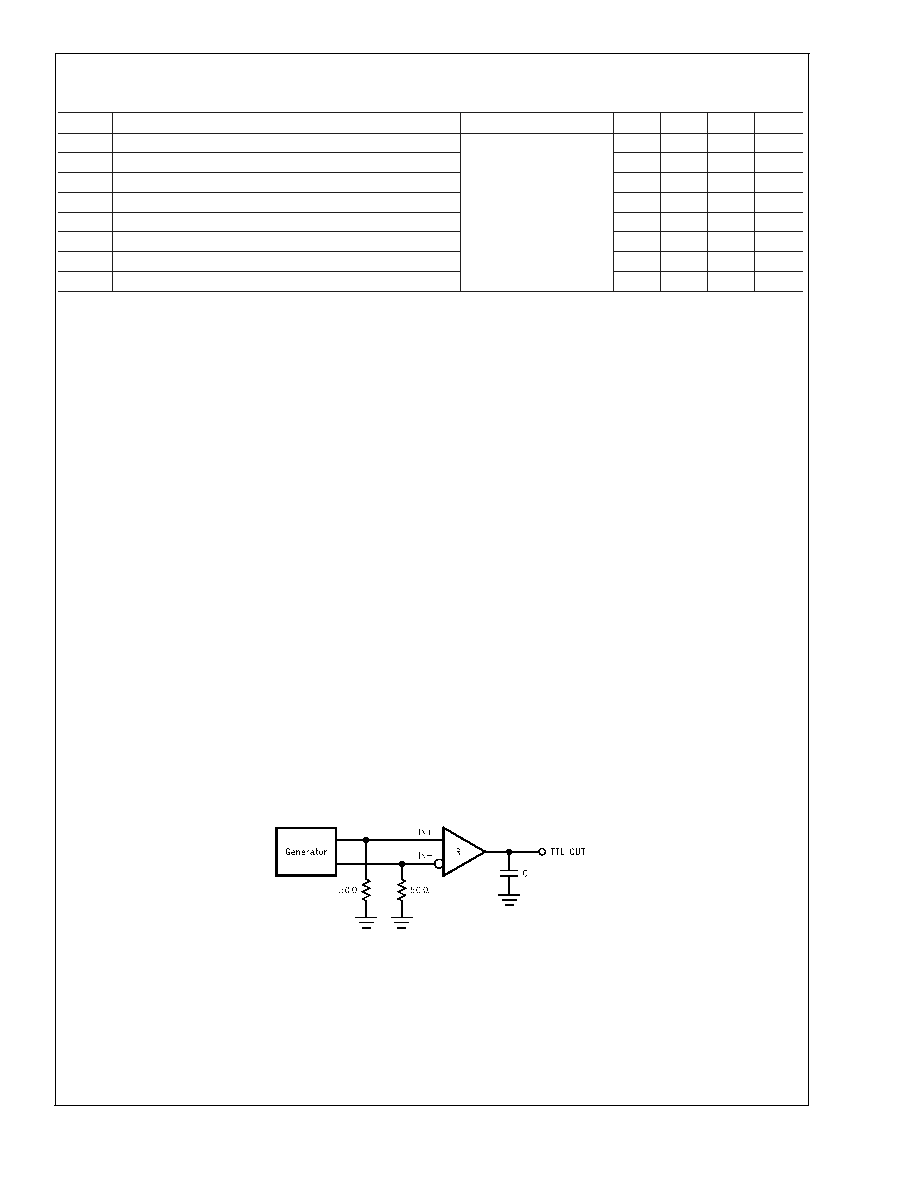
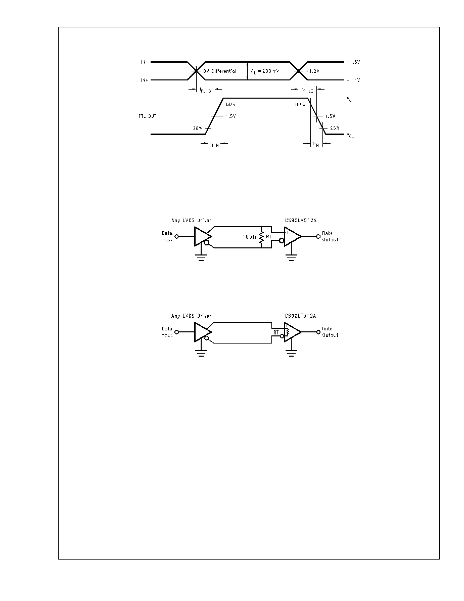
Parameter Measurement Information
20015003
FIGURE 1. Receiver Propagation Delay and Transition Time Test Circuit
DS90L
V012A/DS90L
T012A
www.national.com
3
Parameter Measurement Information
(Continued)
Typical Application
Applications Information
General application guidelines and hints for LVDS drivers
and receivers may be found in the following application
notes: LVDS Owner's Manual (lit #550062-002), AN-808,
AN-977, AN-971, AN-916, AN-805, AN-903.
LVDS drivers and receivers are intended to be primarily used
in an uncomplicated point-to-point configuration as is shown
in Figure 3. This configuration provides a clean signaling
environment for the fast edge rates of the drivers. The re-
ceiver is connected to the driver through a balanced media
which may be a standard twisted pair cable, a parallel pair
cable, or simply PCB traces. Typically the characteristic
impedance of the media is in the range of 100
. A termina-
tion resistor of 100
should be selected to match the media,
and is located as close to the receiver input pins as possible.
The termination resistor converts the driver output (current
mode) into a voltage that is detected by the receiver. Other
configurations are possible such as a multi-receiver configu-
ration, but the effects of a mid-stream connector(s), cable
stub(s), and other impedance discontinuities as well as
ground shifting, noise margin limits, and total termination
loading must be taken into account.
The DS90LV012A and DS90LT012A differential line receiv-
ers are capable of detecting signals as low as 100 mV, over
a
±
1V common-mode range centered around +1.2V. This is
related to the driver offset voltage which is typically +1.2V.
The driven signal is centered around this voltage and may
shift
±
1V around this center point. The
±
1V shifting may be
the result of a ground potential difference between the driv-
er's ground reference and the receiver's ground reference,
the common-mode effects of coupled noise, or a combina-
tion of the two. The AC parameters of both receiver input
pins are optimized for a recommended operating input volt-
age range of 0V to +2.4V (measured from each pin to
ground). The device will operate for receiver input voltages
up to V
DD
, but exceeding V
DD
will turn on the ESD protection
circuitry which will clamp the bus voltages.
20015004
FIGURE 2. Receiver Propagation Delay and Transition Time Waveforms
Balanced System
20015005
FIGURE 3. Point-to-Point Application (DS90LV012A)
Balanced System
20015028
FIGURE 4. Point-to-Point Application (DS90LT012A)
DS90L
V012A/DS90L
T012A
www.national.com
4
Applications Information
(Continued)
Power Decoupling Recommendations:
Bypass capacitors must be used on power pins. Use high
frequency ceramic (surface mount is recommended) 0.1µF
and 0.001µF capacitors in parallel at the power supply pin
with the smallest value capacitor closest to the device supply
pin. Additional scattered capacitors over the printed circuit
board will improve decoupling. Multiple vias should be used
to connect the decoupling capacitors to the power planes. A
10µF (35V) or greater solid tantalum capacitor should be
connected at the power entry point on the printed circuit
board between the supply and ground.
PC Board considerations:
Use at least 4 PCB board layers (top to bottom): LVDS
signals, ground, power, TTL signals.
Isolate TTL signals from LVDS signals, otherwise the TTL
signals may couple onto the LVDS lines. It is best to put TTL
and LVDS signals on different layers which are isolated by a
power/ground plane(s).
Keep drivers and receivers as close to the (LVDS port side)
connectors as possible.
For PC board considerations for the LLP package, please
refer to application note AN-1187 "Leadless Leadframe
Package." It is important to note that to optimize signal
integrity (minimize jitter and noise coupling), the LLP thermal
land pad, which is a metal (normally copper) rectangular
region located under the package, should be attached to
ground and match the dimensions of the exposed pad on the
PCB (1:1 ratio).
Differential Traces:
Use controlled impedance traces which match the differen-
tial impedance of your transmission medium (ie. cable) and
termination resistor. Run the differential pair trace lines as
close together as possible as soon as they leave the IC
(stubs should be
<
10mm long). This will help eliminate
reflections and ensure noise is coupled as common-mode.
In fact, we have seen that differential signals which are 1mm
apart radiate far less noise than traces 3mm apart since
magnetic field cancellation is much better with the closer
traces. In addition, noise induced on the differential lines is
much more likely to appear as common-mode which is re-
jected by the receiver.
Match electrical lengths between traces to reduce skew.
Skew between the signals of a pair means a phase differ-
ence between signals which destroys the magnetic field
cancellation benefits of differential signals and EMI will re-
sult! (Note that the velocity of propagation, v = c/E
r
where c
(the speed of light) = 0.2997mm/ps or 0.0118 in/ps). Do not
rely solely on the autoroute function for differential traces.
Carefully review dimensions to match differential impedance
and provide isolation for the differential lines. Minimize the
number of vias and other discontinuities on the line.
Avoid 90∞ turns (these cause impedance discontinuities).
Use arcs or 45∞ bevels.
Within a pair of traces, the distance between the two traces
should be minimized to maintain common-mode rejection of
the receivers. On the printed circuit board, this distance
should remain constant to avoid discontinuities in differential
impedance. Minor violations at connection points are allow-
able.
Termination:
DS90LV012A:
Use a termination resistor which best matches the differen-
tial impedance or your transmission line. The resistor should
be between 90
and 130. Remember that the current
mode outputs need the termination resistor to generate the
differential voltage. LVDS will not work without resistor ter-
mination. Typically, connecting a single resistor across the
pair at the receiver end will suffice.
Surface mount 1% - 2% resistors are the best. PCB stubs,
component lead, and the distance from the termination to the
receiver inputs should be minimized. The distance between
the termination resistor and the receiver should be
<
10mm
(12mm MAX).
DS90LT012A:
The DS90LT012A integrates the terminating resistor for
point-to-point applications. The resistor value will be be-
tween 90
and 133.
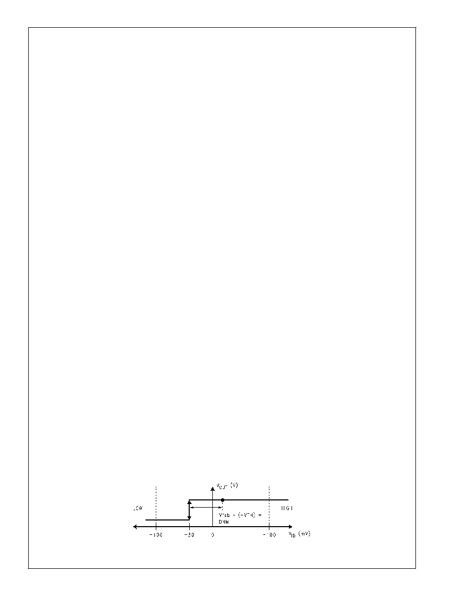
Threshold:
The LVDS Standard (ANSI/TIA/EIA-644-A) specifies a maxi-
mum threshold of
±
100mV for the LVDS receiver. The
DS90LV012A and DS90LT012A support an enhanced
threshold region of -100mV to 0V. This is useful for fail-safe
biasing. The threshold region is shown in the Voltage Trans-
fer Curve (VTC) in Figure 5. The typical DS90LV012A or
DS90LT012A LVDS receiver switches at about -30mV. Note
that with V
ID
= 0V, the output will be in a HIGH state. With an
external fail-safe bias of +25mV applied, the typical differen-
tial noise margin is now the difference from the switch point
to the bias point. In the example below, this would be 55mV
of Differential Noise Margin (+25mV - (-30mV)). With the
enhanced threshold region of -100mV to 0V, this small
external fail-safe biasing of +25mV (with respect to 0V) gives
a DNM of a comfortable 55mV. With the standard threshold
region of
±
100mV, the external fail-safe biasing would need
to be +25mV with respect to +100mV or +125mV, giving a
DNM of 155mV which is stronger fail-safe biasing than is
necessary for the DS90LV012A or DS90LT012A. If more
DNM is required, then a stronger fail-safe bias point can be
set by changing resistor values.
20015029
FIGURE 5. VTC of the DS90LV012A and DS90LT012A LVDS Receivers
DS90L
V012A/DS90L
T012A
www.national.com
5