
DS90LV027AH
High Temperature LVDS Dual Differential Driver
General Description
The DS90LV027AH is a dual LVDS driver device optimized
for high data rate and low power applications. The device is
designed to support data rates in excess of 600Mbps
(300MHz) utilizing Low Voltage Differential Signaling (LVDS)
technology. The DS90LV027AH is a current mode driver
allowing power dissipation to remain low even at high fre-
quency. In addition, the short circuit fault current is also
minimized.
The device is in a 8-lead small outline package. The
DS90LV027AH has a flow-through design for easy PCB
layout. The differential driver outputs provides low EMI with
its typical low output swing of 360 mV. It is perfect for high
speed transfer of clock and data. The DS90LV027AH can be
paired
with
its
companion
dual
line
receiver,
the
DS90LV028AH, or with any of National's LVDS receivers, to
provide a high-speed point-to-point LVDS interface.
Features
n
-40∞C to +125∞C operating temperature range
n
>
600 Mbps (300MHz) switching rates
n
0.3 ns typical differential skew
n
0.7 ns maximum differential skew
n
3.3V power supply design
n
Low power dissipation (46 mW
@
3.3V static)
n
Flow-through design simplifies PCB layout
n
Power Off Protection (outputs in high impedance)
n
Conforms to TIA/EIA-644 Standard
n
8-Lead SOIC package saves space
Connection Diagram
Dual-In-Line
20165101
Order Number DS90LV027AHM
See NS Package Number M08A
Functional Diagram
20165102
20165103
September 2005
DS90L
V027AH
High
T
emperature
L
VDS
Dual
Differential
Driver
© 2005 National Semiconductor Corporation
DS201651
www.national.com

Absolute Maximum Ratings
(Note 1)
If Military/Aerospace specified devices are required,
please contact the National Semiconductor Sales Office/
Distributors for availability and specifications.
Supply Voltage (V
CC
)
-0.3V to +4V
Input Voltage (DI)
-0.3V to +3.6V
Output Voltage (DO
±
)
-0.3V to +3.9V
Maximum Package Power Dissipation
@
+25∞C
M Package
1190 mW
Derate M Package
9.5 mW/∞C above +25∞C
Storage Temperature Range
-65∞C to +150∞C
Lead Temperature Range Soldering
(4 sec.)
+260∞C
ESD Ratings
(HBM 1.5 k
, 100 pF)
8kV
(EIAJ 0
, 200 pF)
1000V
(CDM)
1000V
(IEC direct 330
, 150 pF)
4kV
Recommended Operating
Conditions
Min
Typ
Max
Units
Supply Voltage (V
CC
)
3.0
3.3
3.6
V
Temperature (T
A
)
-40
25
+125
∞C
Electrical Characteristics
Over Supply Voltage and Operating Temperature ranges, unless otherwise specified. (Notes 2, 3, 7)
Symbol
Parameter
Conditions
Pin
Min
Typ
Max
Units
DIFFERENTIAL DRIVER CHARACTERISTICS
V
OD
Output Differential Voltage
R
L
= 100
(Figure 1)
DO+,
DO-
250
360
450
mV
V
OD
V
OD
Magnitude Change
1
35
mV
V
OH
Output High Voltage
1.4
1.6
V
V
OL
Output Low Voltage
0.9
1.1
V
V
OS
Offset Voltage
1.125
1.2
1.375
V
V
OS
Offset Magnitude Change
0
3
25
mV
I
OXD
Power-off Leakage
V
OUT
= V
CC
or GND, V
CC
= 0V
±
1
±
10
µA
I
OSD
Output Short Circuit Current
-5.7
-8
mA
V
IH
Input High Voltage
DI
2.0
V
CC
V
V
IL
Input Low Voltage
GND
0.8
V
I
IH
Input High Current
V
IN
= 3.3V or 2.4V
±
2
±
10
µA
I
IL
Input Low Current
V
IN
= GND or 0.5V
±
1
±
10
µA
V
CL
Input Clamp Voltage
I
CL
= -18 mA
-1.5
-0.6
V
I
CC
Power Supply Current
No Load
V
IN
= V
CC
or GND
V
CC
8
14
mA
R
L
= 100
14
20
mA
Switching Characteristics
Over Supply Voltage and Operating Temperature Ranges, unless otherwise specified. (Notes 3, 4, 5, 6)
Symbol
Parameter
Conditions
Min
Typ
Max
Units
DIFFERENTIAL DRIVER CHARACTERISTICS
t
PHLD
Differential Propagation Delay High to Low
R
L
= 100
, C
L
= 15 pF
0.3
0.8
2.0
ns
t
PLHD
Differential Propagation Delay Low to High
(Figure 2 and Figure 3)
0.3
1.1
2.0
ns
t
SKD1
Differential Pulse Skew |t
PHLD
- t
PLHD
| (Note 8)
0
0.3
0.7
ns
t
SKD2
Channel to Channel Skew (Note 9)
0
0.4
0.8
ns
t
SKD3
Differential Part to Part Skew (Note 10)
0
1.0
ns
t
SKD4
Differential Part to Part Skew (Note 11)
0
1.2
ns
t
TLH
Transition Low to High Time
0.2
0.5
1.0
ns
t
THL
Transition High to Low Time
0.2
0.5
1.0
ns
f
MAX
Maximum Operating Frequency (Note 12)
350
MHz
Note 1: "Absolute Maximum Ratings" are those values beyond which the safety of the device cannot be guaranteed. They are not meant to imply that the devices
should be operated at these limits. The table of "Electrical Characteristics" specifies conditions of device operation.
Note 2: Current into device pins is defined as positive. Current out of device pins is defined as negative. All voltages are referenced to ground except V
OD
.
Note 3: All typicals are given for: V
CC
= +3.3V and T
A
= +25∞C.
Note 4: These parameters are guaranteed by design. The limits are based on statistical analysis of the device over PVT (process, voltage, temperature) ranges.
Note 5: C
L
includes probe and fixture capacitance.
DS90L
V027AH
www.national.com
2

Switching Characteristics
(Continued)
Note 6: Generator waveform for all tests unless otherwise specified: f = 1 MHz, Z
O
= 50
, t
r
1 ns, t
f
1 ns (10%-90%).
Note 7: The DS90LV027AH is a current mode device and only function with datasheet specification when a resistive load is applied to the drivers outputs.
Note 8: t
SKD1
, |t
PHLD
- t
PLHD
|, is the magnitude difference in differential propagation delay time between the positive going edge and the negative going edge of
the same channel.
Note 9: t
SKD2
is the Differential Channel to Channel Skew of any event on the same device.
Note 10: t
SKD3
, Differential Part to Part Skew, is defined as the difference between the minimum and maximum specified differential propagation delays. This
specification applies to devices at the same V
CC
and within 5∞C of each other within the operating temperature range.
Note 11: t
SKD4
, part to part skew, is the differential channel to channel skew of any event between devices. This specification applies to devices over recommended
operating temperature and voltage ranges, and across process distribution. t
SKD4
is defined as |Max - Min| differential propagation delay.
Note 12: f
MAX
generator input conditions: t
r
= t
f
<
1 ns (0% to 100%), 50% duty cycle, 0V to 3V. Output criteria: duty cycle = 45%/55%, V
OD
>
250mV, all channels
switching.
Parameter Measurement Information
20165104
FIGURE 1. Differential Driver DC Test Circuit
20165105
FIGURE 2. Differential Driver Propagation Delay and Transition Time Test Circuit
20165106
FIGURE 3. Differential Driver Propagation Delay and Transition Time Waveforms
DS90L
V027AH
www.national.com
3

Application Information
TABLE 1. Device Pin Descriptions
Pin #
Name
Description
2, 3
DI
TTL/CMOS driver input pins
6, 7
DO+
Non-inverting driver output pin
5, 8
DO-
Inverting driver output pin
4
GND
Ground pin
1
V
CC
Positive power supply pin, +3.3V
±
0.3V
Typical Performance Curves
Output High Voltage vs
Power Supply Voltage
Output Low Voltage vs
Power Supply Voltage
20165107
20165108
Output Short Circuit Current vs
Power Supply Voltage
Differential Output Voltage
vs Power Supply Voltage
20165109
20165110
DS90L
V027AH
www.national.com
4
Typical Performance Curves
(Continued)
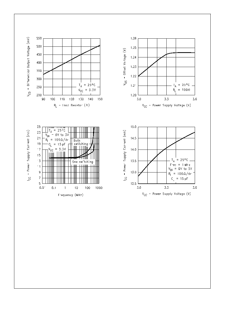
Differential Output Voltage
vs Load Resistor
Offset Voltage vs
Power Supply Voltage
20165111
20165112
Power Supply Current
vs Frequency
Power Supply Current vs
Power Supply Voltage
20165113
20165114
DS90L
V027AH
www.national.com
5