 | –≠–ª–µ–∫—Ç—Ä–æ–Ω–Ω—ã–π –∫–æ–º–ø–æ–Ω–µ–Ω—Ç: DS90LV804 | –°–∫–∞—á–∞—Ç—å:  PDF PDF  ZIP ZIP |
DS90LV804
4-Channel 800 Mbps LVDS Buffer/Repeater
General Description
The DS90LV804 is a four channel 800 Mbps LVDS buffer/
repeater. In many large systems, signals are distributed
across cables and signal integrity is highly dependent on the
data rate, cable type, length, and the termination scheme. In
order to maximize signal integrity, the DS90LV804 features
both an internal input and output (source) termination to
eliminate these extra components from the board, and to
also place the terminations as close as possible to receiver
inputs and driver output. This is especially significant when
driving longer cables.
The DS90LV804, available in the LLP (Leadless Leadframe
Package) package, minimizes the footprint, and improves
system performance.
An output enable pin is provided, which allows the user to
place the LVDS outputs and internal biasing generators in a
TRI-STATE, low power mode.
The differential inputs interface to LVDS, and Bus LVDS
signals such as those on National's 10-, 16-, and 18- bit Bus
LVDS SerDes, as well as CML and LVPECL. The differential
inputs are internally terminated with a 100
resistor to im-
prove performance and minimize board space. This function
function is especially useful for boosting signals over lossy
cables or point-to-point backplane configurations.
Features
n
800 Mbps data rate per channel
n
Low output skew and jitter
n
Hot plug protection
n
LVDS/CML/LVPECL compatible input, LVDS output
n
On-chip 100
input and output termination
n
15 kV ESD protection on LVDS Inputs and Outputs
n
Single 3.3V supply
n
Very low power consumption
n
Industrial -40 to +85∞C temperature range
n
Small LLP Package Footprint
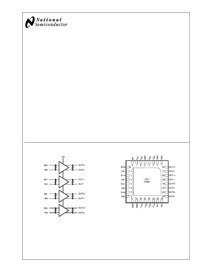
Block and Connection Diagrams
20156701
DS90LV804 Block Diagram
20156702
DS90LV804 LLP Pinout
(Top View)
January 2006
DS90L
V804
4-Channel
800
Mbps
L
VDS
Buffer/Repeater
© 2006 National Semiconductor Corporation
DS201567
www.national.com

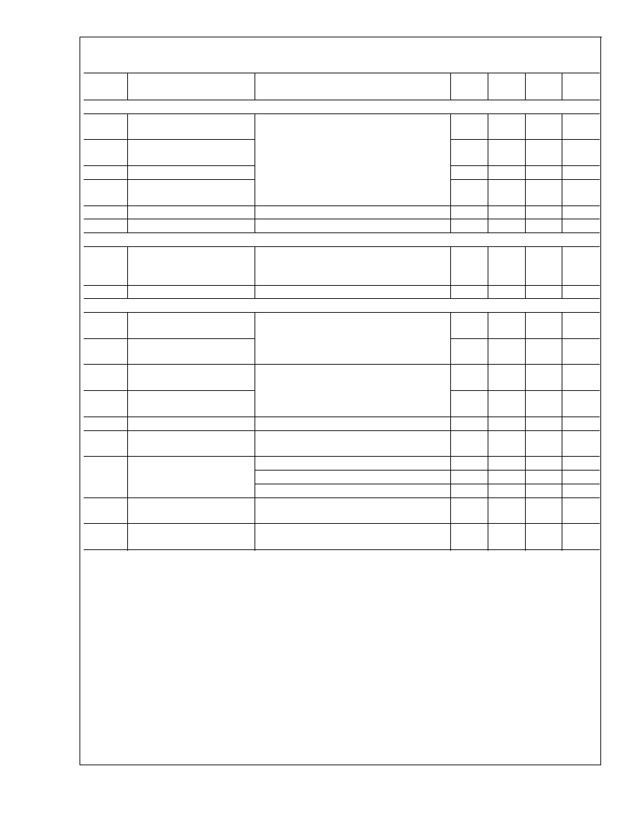
Pin Descriptions
Pin
Name
LLP Pin
Number
I/O, Type
Description
DIFFERENTIAL INPUTS
IN0+
IN0-
9
10
I, LVDS
Channel 0 inverting and non-inverting differential inputs.
IN1+
IN1-
11
12
I, LVDS
Channel 1 inverting and non-inverting differential inputs.
IN2+
IN2-
13
14
I, LVDS
Channel 2 inverting and non-inverting differential inputs.
IN3+
IN3-
15
16
I, LVDS
Channel 3 inverting and non-inverting differential inputs.
DIFFERENTIAL OUTPUTS
OUT0+
OUT0-
32
31
O, LVDS
Channel 0 inverting and non-inverting differential outputs. (Note 2)
OUT1+
OUT1-
30
29
O, LVDS
Channel 1 inverting and non-inverting differential outputs. (Note 2)
OUT2+
OUT2-
28
27
O, LVDS
Channel 2 inverting and non-inverting differential outputs. (Note 2)
OUT3+
OUT3-
26
25
O, LVDS
Channel 3 inverting and non-inverting differential outputs. (Note 2)
DIGITAL CONTROL INTERFACE
EN
8
I, LVTTL
Enable pin. When EN is LOW, the driver is disabled and the LVDS outputs are in
TRI-STATE. When EN is HIGH, the driver is enabled. LVCMOS/LVTTL level input.
POWER
V
DD
3, 4, 6, 7, 19, 20,
21, 22
I, Power
V
DD
= 3.3V,
±
5%
GND
1, 2, 5, 17, 18
(Note 1)
I, Power
Ground reference for LVDS and CMOS circuitry. For the LLP package, the DAP is
used as the primary GND connection to the device. The DAP is the exposed metal
contact at the bottom of the LLP-32 package. It should be connected to the ground
plane with at least 4 vias for optimal AC and thermal performance. The pin numbers
listed should also be tied to ground for proper biasing.
N/C
23, 24
No Connect
Note 1: Note that for the LLP package the GND is connected thru the DAP on the back side of the LLP package in addition to grounding actual pins on the package
as listed.
Note 2: The LVDS outputs do not support a multidrop (BLVDS) environment. The LVDS output characteristics of the DS90LV804 device have been optimized for
point-to-point backplane and cable applications.
DS90L
V804
www.national.com
2

Absolute Maximum Ratings
(Note 3)
Supply Voltage (V
DD
)
-0.3V to +4.0V
CMOS Input Voltage (EN)
-0.3V to (V
DD
+0.3V)
LVDS Receiver Input Voltage
-0.3V to (V
DD
+0.3V)
LVDS Driver Output Voltage
-0.3V to (V
DD
+0.3V)
LVDS Output Short Circuit Current
+90 mA
Junction Temperature
+150∞C
Storage Temperature
-65∞C to +150∞C
Lead Temperature (Solder, 4sec)
260∞C
Max Pkg Power Capacity
@
25∞C
4.16W
Thermal Resistance (
JA
)
30∞C/W
Package Derating above +25∞C
33.3mW/∞C
ESD Last Passing Voltage
HBM, 1.5k
, 100pF
15 kV
EIAJ, 0
, 200pF
250V
Charged Device Model
1000V
Recommended Operating
Conditions
Supply Voltage (V
CC
)
3.15V to 3.45V
Input Voltage (V
I
) (Note 4)
0V to V
DD
Output Voltage (V
O
)
0V to V
DD
Operating Temperature (T
A
)
Industrial
-40∞C to +85∞C
Note 3: Absolute maximum ratings are those values beyond which damage
to the device may occur. The databook specifications should be met, without
exception, to ensure that the system design is reliable over its power supply,
temperature, and output/input loading variables. National does not recom-
mend operation of products outside of recommended operation conditions.
Note 4: V
ID
max
<
2.4V
Electrical Characteristics
Over recommended operating supply and temperature ranges unless other specified.
Symbol
Parameter
Conditions
Min
Typ
(Note 5)
Max
Units
LVTTL DC SPECIFICATIONS (EN)
V
IH
High Level Input Voltage
2.0
V
DD
V
V
IL
Low Level Input Voltage
GND
0.8
V
I
IH
High Level Input Current
V
IN
= V
DD
= V
DDMAX
-10
+10
µA
I
IL
Low Level Input Current
V
IN
= V
SS
, V
DD
= V
DDMAX
-10
+10
µA
C
IN1
Input Capacitance
Any Digital Input Pin to V
SS
3.5
pF
V
CL
Input Clamp Voltage
I
CL
= -18 mA
-1.5
-0.8
V
LVDS INPUT DC SPECIFICATIONS (INn
±
)
V
TH
Differential Input High
Threshold (Note 6)
V
CM
= 0.8V to 3.4V,
V
DD
= 3.45V
0
100
mV
V
TL
Differential Input Low
Threshold (Note 6)
V
CM
= 0.8V to 3.4V,
V
DD
= 3.45V
-100
0
mV
V
ID
Differential Input Voltage
V
CM
= 0.8V to 3.4V, V
DD
= 3.45V
100
2400
mV
V
CMR
Common Mode Voltage Range V
ID
= 150 mV, V
DD
= 3.45V
0.05
3.40
V
C
IN2
Input Capacitance
IN+ or IN- to V
SS
3.5
pF
I
IN
Input Current
V
IN
= 3.45V, V
DD
= V
DDMAX
-10
+10
µA
V
IN
= 0V, V
DD
= V
DDMAX
-10
+10
µA
DS90L
V804
www.national.com
3
Electrical Characteristics
(Continued)
Over recommended operating supply and temperature ranges unless other specified.
Symbol
Parameter
Conditions
Min
Typ
(Note 5)
Max
Units
LVDS OUTPUT DC SPECIFICATIONS (OUTn
±
)
V
OD
Differential Output Voltage
(Note 6)
R
L
= 100
external resistor between OUT+ and
OUT-
250
500
600
mV
V
OD
Change in V
OD
between
Complementary States
-35
35
mV
V
OS
Offset Voltage (Note 7)
1.05
1.18
1.475
V
V
OS
Change in V
OS
between
Complementary States
-35
35
mV
I
OS
Output Short Circuit Current
OUT+ or OUT- Short to GND
-60
-90
mA
C
OUT2
Output Capacitance
OUT+ or OUT- to GND when TRI-STATE
5.5
pF
SUPPLY CURRENT (Static)
I
CC
Total Supply Current
All inputs and outputs enabled and active,
terminated with external differential load of 100
between OUT+ and OUT-.
117
140
mA
I
CCZ
TRI-STATE Supply Current
EN = 0V
2.7
6
mA
SWITCHING CHARACTERISTICS -- LVDS OUTPUTS
t
LHT
Differential Low to High
Transition Time
Use an alternating 1 and 0 pattern at 200 Mbps,
measure between 20% and 80% of V
OD
.
210
300
ps
t
HLT
Differential High to Low
Transition Time
210
300
ps
t
PLHD
Differential Low to High
Propagation Delay
Use an alternating 1 and 0 pattern at 200 Mbps,
measure at 50% V
OD
between input to output.
2.0
3.2
ns
t
PHLD
Differential High to Low
Propagation Delay
2.0
3.2
ns
t
SKD1
Pulse Skew
|t
PLHD
≠t
PHLD
|
25
80
ps
t
SKCC
Output Channel to Channel
Skew
Difference in propagation delay (t
PLHD
or t
PHLD
)
among all output channels.
50
125
ps
t
JIT
Jitter
(Note 8)
RJ - Alternating 1 and 0 at 400 MHz (Note 9)
1.1
1.5
psrms
DJ - K28.5 Pattern, 800 Mbps (Note 10)
15
35
psp-p
TJ - PRBS 2
23
-1 Pattern, 800 Mbps (Note 11)
30
55
psp-p
t
ON
LVDS Output Enable Time
Time from EN to OUT
±
change from
TRI-STATE to active.
300
ns
t
OFF
LVDS Output Disable Time
Time from EN to OUT
±
change from active to
TRI-STATE.
12
ns
Note 5: Typical parameters are measured at V
DD
= 3.3V, T
A
= 25∞C. They are for reference purposes, and are not production-tested.
Note 6: Differential output voltage V
OD
is defined as ABS(OUT+≠OUT-). Differential input voltage V
ID
is defined as ABS(IN+≠IN-).
Note 7: Output offset voltage V
OS
is defined as the average of the LVDS single-ended output voltages at logic high and logic low states.
Note 8: Jitter is not production tested, but guaranteed through characterization on a sample basis.
Note 9: Random Jitter, or RJ, is measured RMS with a histogram including 1500 histogram window hits. The input voltage = V
ID
= 500mV, 50% duty cycle at 400
MHz, t
r
= t
f
= 50ps (20% to 80%).
Note 10: Deterministic Jitter, or DJ, is measured to a histogram mean with a sample size of 350 hits. The input voltage = V
ID
= 500mV, K28.5 pattern at 800 Mbps,
t
r
= t
f
= 50ps (20% to 80%). The K28.5 pattern is repeating bit streams of (0011111010 1100000101).
Note 11: Total Jitter, or TJ, is measured peak to peak with a histogram including 3500 window hits. Stimulus and fixture Jitter has been subtracted. The input voltage
= V
ID
= 500mV, 2
23
-1 PRBS pattern at 800 Mbps, t
r
= t
f
= 50ps (20% to 80%).
DS90L
V804
www.national.com
4
Feature Descriptions
INTERNAL TERMINATIONS
The DS90LV804 has integrated termination resistors on both
the input and outputs. The inputs have a 100
resistor
across the differential pair, placing the receiver termination
as close as possible to the input stage of the device. The
LVDS outputs also contain an integrated 100
ohm termi-
nation resistor, this resistor is used to reduce the effects of
Near End Crosstalk (NEXT) and does not take the place of
the 100 ohm termination at the inputs to the receiving device.
The integrated terminations improve signal integrity and de-
crease the external component count resulting in space
savings.
OUTPUT CHARACTERISTICS
The output characteristics of the DS90LV804 have been
optimized for point-to-point backplane and cable applica-
tions, and are not intended for multipoint or multidrop signal-
ing.
TRI-STATE MODE
The EN input activates a hardware TRI-STATE mode. When
the TRI-STATE mode is active (EN=L), all input and output
buffers and internal bias circuitry are powered off and dis-
abled. Outputs are tri-stated in TRI-STATE mode. When
exiting TRI-STATE mode, there is a delay associated with
turning on bandgap references and input/output buffer cir-
cuits as indicated in the LVDS Output Switching Character-
istics
INPUT FAILSAFE BIASING
External pull up and pull down resistors may be used to
provide enough of an offset to enable an input failsafe under
open-circuit conditions. This configuration ties the positive
LVDS input pin to V
DD
thru a pull up resistor and the negative
LVDS input pin is tied to GND by a pull down resistor. The
pull up and pull down resistors should be in the 5k
to 15k
range to minimize loading and waveform distortion to the
driver. The common-mode bias point ideally should be set to
approximately 1.2V (less than 1.75V) to be compatible with
the internal circuitry. Please refer to application note AN-
1194 "Failsafe Biasing of LVDS Interfaces" for more informa-
tion.
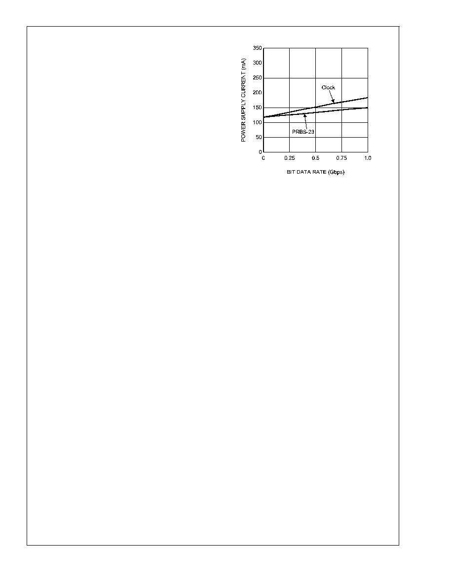
TYPICAL PERFORMANCE CHARACTERISTICS
20156741
Dynamic power supply current was measured while running a clock or
PRBS 2
23
-1 pattern with all 4 channels active. V
CC
= 3.3V, T
A
= +25∞C,
V
ID
= 0.5V, V
CM
= 1.2V
Power Supply Current vs. Bit Data Rate
Packaging Information
The Leadless Leadframe Package (LLP) is a leadframe
based chip scale package (CSP) that may enhance chip
speed, reduce thermal impedance, and reduce the printed
circuit board area required for mounting. The small size and
very low profile make this package ideal for high density
PCBs used in small-scale electronic applications such as
cellular phones, pagers, and handheld PDAs. The LLP pack-
age is offered in the no Pullback configuration. In the no
Pullback configuration the standard solder pads extend and
terminate at the edge of the package. This feature offers a
visible solder fillet after board mounting.
The LLP has the following advantages:
∑
Low thermal resistance
∑
Reduced electrical parasitics
∑
Improved board space efficiency
∑
Reduced package height
∑
Reduced package mass
For more details about LLP packaging technology, refer to
applications note AN-1187, "Leadless Leadframe Package"
DS90L
V804
www.national.com
5