DS92LV040A
4 Channel Bus LVDS Transceiver
General Description
The DS92LV040A is one in a series of Bus LVDS transceiv-
ers designed specifically for high speed, low power back-
plane or cable interfaces. The device operates from a single
3.3V power supply and includes four differential line drivers
and four receivers. To minimize bus loading, the driver out-
puts and receiver inputs are internally connected. The device
also features a flow through pin out which allows easy PCB
routing for short stubs between its pins and the connector.
The driver translates 3V LVTTL levels (single-ended) to dif-
ferential Bus LVDS (BLVDS) output levels. This allows for
high speed operation while consuming minimal power and
reducing EMI. In addition, the differential signaling provides
common mode noise rejection greater than
±
1V.
The receiver threshold is less than +0/-70 mV. The receiver
translates the differential Bus LVDS to standard (LVTTL/
LVCMOS) levels. (See Applications Information Section for
more details.)
Features
n
Bus LVDS Signaling
n
Propagation delay: Driver 2.3ns max, Receiver 3.2ns
max
n
Low power CMOS design
n
100% Transition time 1ns driver typical, 1.3ns receiver
typical
n
High Signaling Rate Capability (above 155 Mbps)
n
0.1V to 2.3V Common Mode Range for V
ID
= 200mV
n
70 mV Receiver Sensitivity
n
Supports open and terminated failsafe on port pins
n
3.3V operation
n
Glitch free power up/down (Driver & Receiver disabled)
n
Light Bus Loading (5 pF typical) per Bus LVDS load
n
Designed for Double Termination Applications
n
Balanced Output Impedance
n
Product offered in 44 pin LLP (Leadless Leadframe
Package) package
n
High impedance Bus pins on power off (V
CC
= 0V)
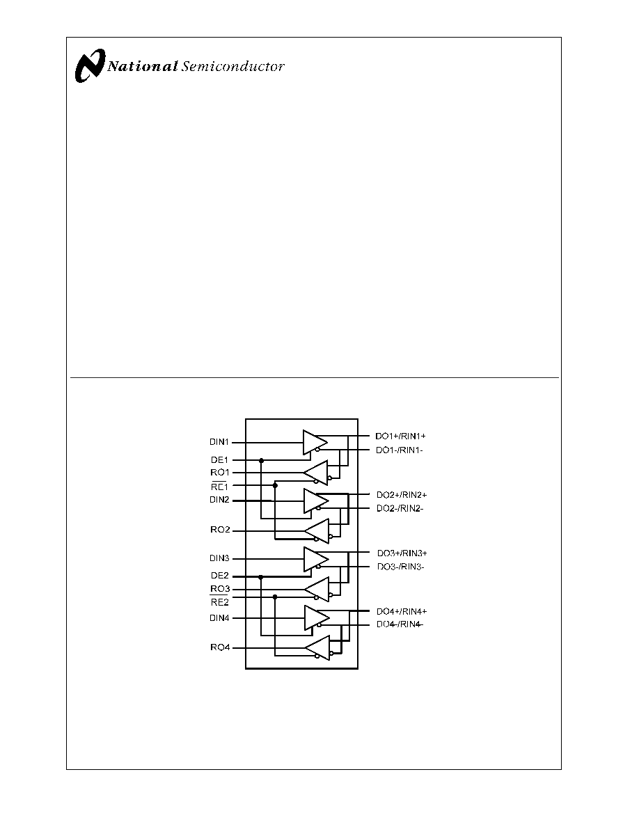
Simplified Functional Diagram
10133601
August 2002
DS92L
V040A
4
Channel
Bus
L
VDS
T
ransceiver
© 2002 National Semiconductor Corporation
DS101336
www.national.com

Absolute Maximum Ratings
(Notes 1,
2)
If Military/Aerospace specified devices are required,
please contact the National Semiconductor Sales Office/
Distributors for availability and specifications.
Supply Voltage (V
CC
)
4.0V
Enable Input Voltage
(DE, RE)
-0.3V to (V
CC
+0.3V)
Driver Input Voltage (D
IN
)
-0.3V to (V
CC
+0.3V)
Receiver Output Voltage
(R
OUT
)
-0.3V to (V
CC
+0.3V)
Bus Pin Voltage (DO/RI
±
)
-0.3V to +3.9V
ESD (Note 4)
(HBM 1.5 k
, 100 pF)
>
4kV
Machine Model
>
250V
Maximum Package Power Dissipation at 25∞C
LLP(Note 3)
4.8 W
Derate LLP Package
38.8mW/∞C
ja
(Note 3)
25.8∞C/W
jc
25.5∞C/W
Storage Temperature Range
-65∞C to +150∞C
Lead Temperature
(Soldering, 4 sec.)
260∞C
Recommended Operating
Conditions
Min
Max
Units
Supply Voltage (V
CC
)
3.0
3.6
V
Receiver Input Voltage
0.0
2.4
V
Operating Free Air Temperature
-40
+85
∞C
Slowest Input Edge Rate
(Note 7)(20% to 80%)
t/V
Data
1.0
ns/V
Control
3.0
ns/V
DC Electrical Characteristics
Over recommended operating supply voltage and temperature ranges unless otherwise specified (Notes 2, 4)
Symbol
Parameter
Conditions
Pin
Min
Typ
Max
Units
V
OD
Output Differential
Voltage
R
L
= 27
, Figure 1
DO+/RI+,
DO-/RI-
200
300
460
mV
V
OD
V
OD
Magnitude Change
5
27
mV
V
OS
Offset Voltage
1.1
1.3
1.5
V
V
OS
Offset Magnitude Change
5
10
mV
V
OHD
Driver Output High
Voltage
R
L
= 27
1.4
1.65
V
V
OLD
Driver Output Low
Voltage
R
L
= 27
0.95
1.1
V
I
OSD
Driver Output Short
Circuit Current (Note 11)
V
OD
= 0V, DE = V
CC
, Driver outputs
shorted together
|30|
| 45|
mA
V
OHR
Receiver Voltage Output
High (Note 12)
V
ID
= +300 mV
I
OH
= -4 mA
R
OUT
V
CC
-0.2
V
Inputs Open
V
CC
-0.2
V
Inputs Terminated,
R
L
= 27
V
CC
-0.2
V
V
OLR
Receiver Voltage Output
Low
I
OL
= 4.0 mA, V
ID
= -300 mV
0.05
0.100
V
I
OD
Receiver Output Dynamic
Current (Note 11)
V
ID
= 300mV, V
OUT
= V
CC
-1.0V
-50
|33|
mA
V
ID
= -300mV, V
OUT
= 1.0V
|36|
60
mA
V
TH
Input Threshold High
(Note 9)
DE = 0V, Over common mode range
DO+/RI+,
DO-/RI-
-40
0
mV
V
TL
Input Threshold Low
(Note 9)
-70
-40
mV
V
CMR
Receiver Common Mode
Range
|V
ID
|/2
2.4 -
|V
ID
|/2
V
I
IN
Input Current
DE = 0V, RE = 2.4V,
V
IN
= +2.4V or 0V
-20
±
1
+20
µA
V
CC
= 0V, V
IN
= +2.4V or 0V
-20
±
1
+20
µA
DS92L
V040A
www.national.com
2
DC Electrical Characteristics
(Continued)
Over recommended operating supply voltage and temperature ranges unless otherwise specified (Notes 2, 4)
Symbol
Parameter
Conditions
Pin
Min
Typ
Max
Units
V
IH
Minimum Input High
Voltage
D
IN
, DE,
RE
2.0
V
CC
V
V
IL
Maximum Input Low
Voltage
GND
0.8
V
I
IH
Input High Current
V
IN
= V
CC
or 2.4V
-20
±
2.5
+20
µA
I
IL
Input Low Current
V
IN
= GND or 0.4V
-20
±
2.5
+20
µA
V
CL
Input Diode Clamp
Voltage
I
CLAMP
= -18 mA
-1.5
-0.8
V
I
CCD
Power Supply Current
Drivers Enabled,
Receivers Disabled
No Load, DE = RE = V
CC
,
DIN = V
CC
or GND
V
CC
20
40
mA
I
CCR
Power Supply Current
Drivers Disabled,
Receivers Enabled
DE = RE = 0V, V
ID
=
±
300mV
27
40
mA
I
CCZ
Power Supply Current,
Drivers and Receivers
TRI-STATE
DE = 0V; RE = V
CC
,
DIN = V
CC
or GND
28
40
mA
I
CC
Power Supply Current,
Drivers and Receivers
Enabled
DE = V
CC
; RE = 0V,
DIN = V
CC
or GND,
R
L
= 27
70
100
mA
I
OFF
Power Off Leakage
Current
V
CC
= 0V or OPEN,
D
IN
, DE, RE = 0V or OPEN,
V
APPLIED
= 3.6V (Port Pins)
DO+/RI+,
DO-/RI-
-20
+20
µA
C
OUTPUT
Capacitance
@
Bus Pins
DO+/RI+,
DO-/RI-
5
pF
c
OUTPUT
Capacitance
@
R
OUT
R
OUT
5
pF
AC Electrical Characteristics
Over recommended operating supply voltage and temperature ranges unless otherwise specified (Note 7)
Symbol
Parameter
Conditions
Min
Typ
Max
Units
DIFFERENTIAL DRIVER TIMING REQUIREMENTS
t
PHLD
Differential Prop. Delay High to Low (Note 9)
R
L
= 27
,
Figures 2, 3,
C
L
= 10 pF
1.0
1.5
2.3
ns
t
PLHD
Differential Prop. Delay Low to High (Note 9)
1.0
1.5
2.3
ns
t
SKD1
Differential Skew |t
PHLD
≠t
PLHD
| (duty cycle)(Note 10),
(Note 9)
80
160
ps
t
CCSK
Channel to Channel Skew (all 4 channels), (Note 9)
220
400
ps
t
TLH
Transition Time Low to High (20% to 80%)
0.4
0.75
1.3
ns
t
THL
Transition Time High to Low (80% to 20%)
0.4
0.75
1.3
ns
t
PHZ
Disable Time High to Z
R
L
= 27
,
Figures 4, 5,
C
L
= 10 pF
5.0
10
ns
t
PLZ
Disable Time Low to Z
5.0
10
ns
t
PZH
Enable Time Z to High
5.0
10
ns
t
PZL
Enable Time Z to Low
5.0
10
ns
f
MAXD
Guaranteed operation per data sheet up to the Min.
Duty Cycle 45/55%,Transition time
25% of period
(Note 9)
85
125
MHz
DS92L
V040A
www.national.com
3
AC Electrical Characteristics
(Continued)
Over recommended operating supply voltage and temperature ranges unless otherwise specified (Note 7)
Symbol
Parameter
Conditions
Min
Typ
Max
Units
DIFFERENTIAL RECEIVER TIMING REQUIREMENTS
t
PHLDR
Differential Prop. Delay High to Low (Note 9)
Figures 6, 7,
C
L
= 15 pF
1.6
2.4
3.2
ns
t
PLHDR
Differential Prop Delay Low to High (Note 9)
1.6
2.4
3.2
ns
t
SDK1R
Differential Skew |t
PHLD
≠t
PLHD
| (duty cycle)(Note 10),
(Note 9)
85
160
ps
t
CCSKR
Channel to Channel Skew (all 4 channels)(Note 9)
140
300
ps
t
TLHR
Transition Time Low to High (10% to 90%) (Note 9)
0.850
1.250
2.0
ns
t
THLR
Transition Time High to Low (90% to 10%) (Note 9)
0.850
1.030
2.0
ns
t
PHZ
Disable Time High to Z
R
L
= 500
,
Figures 8, 9,
C
L
= 15 pF
3.0
10
ns
t
PLZ
Disable Time Low to Z
3.0
10
ns
t
PZH
Enable Time Z to High
3.0
10
ns
t
PZL
Enable Time Z to Low
3.0
10
ns
f
MAXR
Guaranteed operation per data sheet up to the Min.
Duty Cycle 45/55%,Transition time
25% of period
(Note 9)
85
125
MHz
Note 1: "Absolute Maximum Ratings" are those values beyond which the safety of the device cannot be guaranteed. They are not meant to imply that the devices
should be operated at these limits. The table of "Electrical Characteristics" provides conditions for actual device operation.
Note 2: All currents into device pins are positive; all currents out of device pins are negative. All voltages are referenced to ground unless otherwise specified except
V
OD
,
V
OD
and V
ID
.
Note 3: Package must be mounted to pc board in accordance with AN-1187 to achieve thermals.
Note 4: All typicals are given for V
CC
= +3.3V and T
A
= +25∞C, unless otherwise stated.
Note 5: ESD Rating: HBM (1.5 k
, 100 pF)
>
4 kV EIAJ (0
, 200 pF)
>
250.
Note 6: C
L
includes probe and fixture capacitance.
Note 7: Generator waveforms for all tests unless otherwise specified: f = 25 MHz, Z
O
= 50
, t
r
, t
f
=
<
1.0 ns (0%≠100%). To ensure fastest propagation delay and
minimum skew, data input edge rates should be equal to or faster than 1ns/V; control signals equal to or faster than 3ns/V. In general, the faster the input edge rate,
the better the AC performance.
Note 8: The DS92LV040A functions within datasheet specification when a resistive load is applied to the driver outputs.
Note 9: Propagation delays, transition times, and receiver threshold are guaranteed by design and characterization.
Note 10: t
SKD1
|t
PHLD
≠t
PLHD
| is the worst case pulse skew (measure of duty cycle) over recommended operation conditions.
Note 11: Only one output at a time should be shorted, do not exceed maximum package power dissipation capacity.
Note 12: V
OH
fail-safe terminated test performed with 27
connected between RI+ and RI- inputs. No external voltage is applied.
Note 13: Chip to Chip skew is the difference in differential propagation delay between any channels of any devices, either edge.
Applications Information
General application guidelines and hints may be found in the
following application notes: AN-808, AN-977, AN-971, and
AN-903.
BLVDS drivers and receivers are intended to be used in a
differential backplane configuration. Transceivers or receiv-
ers are connected to the driver through a balanced media
such as differential PCB traces. Typically, the characteristic
differential impedance of the media (Zo) is in the range of
50
to 100. Two termination resistors of Zo each are
placed at the ends of the transmission line backplane. The
termination resistor converts the current sourced by the
driver into a voltage that is detected by the receiver. The
effects of mid-stream connector(s), cable stub(s), and other
impedance discontinuity as well as ground shifting, noise
margin limits, and total termination loading must be taken
into account. The DS92LV040A differential line driver is a
balanced current mode design. A current mode driver, gen-
erally speaking has a high output impedance (100 ohms)
and supplies a reasonably constant current for a range of
loads (a voltage mode driver on the other hand supplies a
constant voltage for a range of loads). Current is switched
through the load in one direction to produce a logic state and
in the other direction to produce the other logic state. The
output current is typically 12 mA. The current changes as a
function of load resistor. The current mode requires (as
discussed above) that a resistive termination be employed to
terminate the signal and to complete the loop. Unterminated
configurations are not allowed. The 12 mA loop current will
develop a differential voltage of about 300mV across a 27
(double terminated 54
differential transmission backplane)
effective resistance, which the receiver detects with a 230
mV minimum differential noise margin neglecting resistive
line losses (driven signal minus receiver threshold (300 mV
≠ 70 mV = 230 mV)). The signal is centered around +1.2V
(Driver Offset, VOS ) with respect to ground. Note that the
steady-state voltage (VSS ) peak-to-peak swing is twice the
differential voltage (VOD ) and is typically 600 mV. The
current mode driver provides substantial benefits over volt-
age mode drivers, such as an RS-422 driver. Its quiescent
current remains relatively flat versus switching frequency.
Whereas the RS-422 voltage mode driver increases expo-
nentially in most case between 20 MHz≠50 MHz. This is due
to the overlap current that flows between the rails of the
device when the internal gates switch. Whereas the current
mode driver switches a fixed current between its output
without any substantial overlap current. This is similar to
some ECL and PECL devices, but without the heavy static
ICC requirements of the ECL/PECL designs. LVDS requires
80% less current than similar PECL devices. AC specifica-
tions for the driver are a tenfold improvement over other
DS92L
V040A
www.national.com
4

Applications Information
(Continued)
existing RS-422 drivers. The TRI-STATE function allows the
driver outputs to be disabled, thus obtaining an even lower
power state when the transmission of data is not required.
There are a few common practices which should be implied
when designing PCB for Bus LVDS signaling. Recom-
mended practices are:
∑
Use at least 4 PCB board layer (Bus LVDS signals,
ground, power and TTL signals).
∑
Keep drivers and receivers as close to the (Bus LVDS
port side) connector as possible.
∑
Bypass each Bus LVDS device and also use distributed
bulk capacitance between power planes. Surface mount
capacitors placed close to power and ground pins work
best. Three or more high frequency, multi-layer ceramic
(MLC) surface mount (0.1 µF, 0.01 µF, 0.001 µF) in
parallel should be used between each V
CC
and ground.
Multiple vias should be used to connect V
CC
and Ground
planes to the pads of the by-pass capacitors.
In addition, it may be necessary to randomly distribute
by-pass capacitors of different values (200pF to 1000pF)
to achieve different resonant frequencies.
∑
Use the termination resistor which best matches the dif-
ferential impedance of your transmission line.
∑
Leave unused Bus LVDS receiver inputs open (floating).
Limit traces on unused inputs to
<
0.5 inches.
∑
Isolate TTL signals from Bus LVDS signals
MEDIA (CONNECTOR or BACKPLANE) SELECTION:
∑
The backplane and connectors should have a matched
differential impedance. Use controlled impedance traces
which match the differential impedance of your transmis-
sion medium (ie. backplane or cable) and termination
resistor(s). Run the differential pair trace lines as close
together as possible as soon as they leave the IC . This
will help eliminate reflections and ensure noise is coupled
as common-mode. In fact, we have seen that differential
signals which are 1mm apart radiate far less noise than
traces 3mm apart since magnetic field cancellation is
much better with the closer traces. Plus, noise induced
on the differential lines is much more likely to appear as
common-mode which is rejected by the receiver. Match
electrical lengths between traces to reduce skew. Skew
between the signals of a pair means a phase difference
between signals which destroys the magnetic field can-
cellation benefits of differential signals and EMI will re-
sult. (Note the velocity of propagation, v = c/Er where c
(the speed of light) = 0.2997mm/ps or 0.0118 in/ps). Do
not rely solely on the autoroute function for differential
traces. Carefully review dimensions to match differential
impedance and provide isolation for the differential lines.
Minimize the number of vias and other discontinuity on
the line. Avoid 90∞ turns (these cause impedance discon-
tinuity). Use arcs or 45∞ bevels. Within a pair of traces,
the distance between the two traces should be minimized
to maintain common-mode rejection of the receivers. On
the printed circuit board, this distance should remain
constant to avoid discontinuity in differential impedance.
Minor violations at connection points are allowable.
∑
Stub Length: Stub lengths should be kept to a minimum.
The typical transition time of the DS92LV040A BLVDS
output is 0.75ns (20% to 80%). The extrapolated 100
percent time is 0.75/0.6 or 1.25ns. For a general approxi-
mation, if the electrical length of a trace is greater than
1/5 of the transition edge, then the trace is considered a
transmission line. For example, 1.25ns/5 is 250 picosec-
onds. Let velocity equal 160ps per inch for a typical
loaded backplane. Then maximum stub length is 250ps/
160ps/in or 1.56 inches. To determine the maximum stub
for your backplane, you need to know the propagation
velocity for the actual conditions (refer to application
notes AN 905 and AN 808).
PACKAGE and SOLDERING INFORMATION:
∑
Refer to packaging application note AN-1187. This appli-
cation note details the package attachment methods to
achieve the correct solderability and thermal results.
DS92L
V040A
www.national.com
5