DS92LV090A
9 Channel Bus LVDS Transceiver
General Description
The DS92LV090A is one in a series of Bus LVDS transceiv-
ers designed specifically for the high speed, low power
proprietary backplane or cable interfaces. The device oper-
ates from a single 3.3V power supply and includes nine
differential line drivers and nine receivers. To minimize bus
loading, the driver outputs and receiver inputs are internally
connected. The separate I/O of the logic side allows for loop
back support. The device also features a flow through pin out
which allows easy PCB routing for short stubs between its
pins and the connector.
The driver translates 3V TTL levels (single-ended) to differ-
ential Bus LVDS (BLVDS) output levels. This allows for high
speed operation, while consuming minimal power with re-
duced EMI. In addition, the differential signaling provides
common mode noise rejection of
±
1V.
The receiver threshold is less than
±
100 mV over a
±
1V
common mode range and translates the differential Bus
LVDS to standard (TTL/CMOS) levels. (See Applications
Information Section for more details.)
Features
n
Bus LVDS Signaling
n
3.2 nanosecond propagation delay max
n
Chip to Chip skew
±
800ps
n
Low power CMOS design
n
High Signaling Rate Capability (above 100 Mbps)
n
0.1V to 2.3V Common Mode Range for V
ID
= 200mV
n
±
100 mV Receiver Sensitivity
n
Supports open and terminated failsafe on port pins
n
3.3V operation
n
Glitch free power up/down (Driver & Receiver disabled)
n
Light Bus Loading (5 pF typical) per Bus LVDS load
n
Designed for Double Termination Applications
n
Balanced Output Impedance
n
Product offered in 64 pin TQFP package
n
High impedance Bus pins on power off (V
CC
= 0V)
n
Driver Channel to Channel skew (same device) 230ps
typical
n
Receiver Channel to Channel skew (same device)
370ps typical
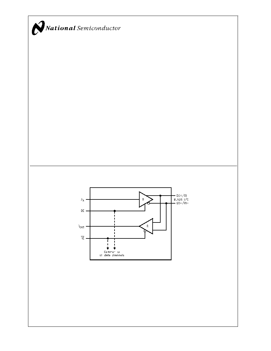
Simplified Functional Diagram
TRI-STATE
Æ
is a registered trademark of National Semiconductor Corporation.
DS100111-1
February 2001
DS92L
V090A
9
Channel
Bus
L
VDS
T
ransceiver
© 2001 National Semiconductor Corporation
DS100111
www.national.com
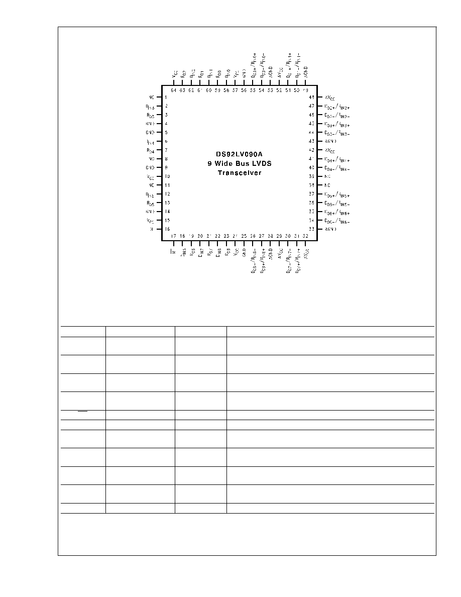
Connection Diagram
Pinout Description
Pin Name
Pin #
Input/Output
Descriptions
DO+/RI+
27, 31, 35, 37, 41,
45, 47, 51, 55
I/O
True Bus LVDS Driver Outputs and Receiver Inputs.
DO-/RI-
26, 30, 34, 36, 40,
44, 46, 50, 54
I/O
Complimentary Bus LVDS Driver Outputs and Receiver Inputs.
D
IN
2, 6, 12, 18, 20, 22,
58, 60, 62
I
TTL Driver Input.
RO
3, 7, 13, 19, 21, 23,
59, 61, 63
O
TTL Receiver Output.
RE
17
I
Receiver Enable TTL Input (Active Low).
DE
16
I
Driver Enable TTL Input (Active High).
GND
4, 5, 9, 14, 25, 56
Power
Ground for digital circuitry (must connect to GND on PC board).
These pins connected internally.
V
CC
10, 15, 24, 57, 64
Power
V
CC
for digital circuitry (must connect to V
CC
on PC board). These
pins connected internally.
AGND
28, 33, 43, 49, 53
Power
Ground for analog circuitry (must connect to GND on PC board).
These pins connected internally.
AV
CC
29, 32, 42, 48, 52
Power
Analog V
CC
(must connect to V
CC
on PC board). These pins
connected internally.
NC
1, 8, 11, 38, 39
N/A
Leave open circuit, do not connect.
DS100111-2
Top View
Order Number DS92LV090ATVEH
See NS Package Number VEH064DB
DS92L
V090A
www.national.com
2
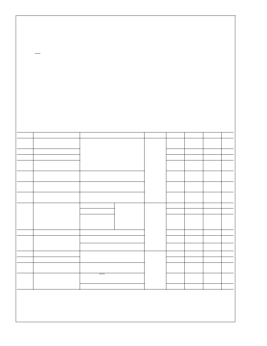
Absolute Maximum Ratings
(Notes 1, 2)
If Military/Aerospace specified devices are required,
please contact the National Semiconductor Sales Office/
Distributors for availability and specifications.
Supply Voltage (V
CC
)
4.0V
Enable Input Voltage
(DE, RE)
-0.3V to (V
CC
+0.3V)
Driver Input Voltage (D
IN
)
-0.3V to (V
CC
+0.3V)
Receiver Output Voltage
(R
OUT
)
-0.3V to (V
CC
+0.3V)
Bus Pin Voltage (DO/RI
±
)
-0.3V to +3.9V
ESD (HBM 1.5 k
, 100 pF)
>
4.5 kV
Driver Short Circuit Duration
momentary
Receiver Short Circuit
Duration
momentary
Maximum Package Power Dissipation at 25∞C
TQFP
1.74 W
Derate TQFP Package
13.9 mW/∞C
ja
71.7∞C/W
jc
10.9∞C/W
Storage Temperature
Range
-65∞C to +150∞C
Lead Temperature
(Soldering, 4 sec.)
260∞C
Recommended Operating
Conditions
Min
Max
Units
Supply Voltage (V
CC
)
3.0
3.6
V
Receiver Input Voltage
0.0
2.4
V
Operating Free Air Temperature
-40
+85
∞C
Maximum Input Edge Rate
(Note 6)(20% to 80%)
t/
V
Data
1.0
ns/V
Control
3.0
ns/V
DC Electrical Characteristics
Over recommended operating supply voltage and temperature ranges unless otherwise specified (Notes 2, 3)
Symbol
Parameter
Conditions
Pin
Min
Typ
Max
Units
V
OD
Output Differential
Voltage
R
L
= 27
,
Figure 1
DO+/RI+,
DO-/RI-
240
300
460
mV
V
OD
V
OD
Magnitude Change
27
mV
V
OS
Offset Voltage
1.1
1.3
1.5
V
V
OS
Offset Magnitude
Change
5
10
mV
V
OH
Driver Output High
Voltage
R
L
= 27
1.4
1.65
V
V
OL
Driver Output Low
Voltage
R
L
= 27
0.95
1.1
V
I
OSD
Output Short Circuit
Current (Note 10)
V
OD
= 0V, DE = V
CC
, Driver
outputs shorted together
|36|
|65|
mA
V
OH
Voltage Output High
(Note 11)
V
ID
= +300 mV
I
OH
= -400 µA
R
OUT
V
CC
-0.2
V
Inputs Open
V
CC
-0.2
V
Inputs
Terminated,
R
L
= 27
V
CC
-0.2
V
V
OL
Voltage Output Low
I
OL
= 2.0 mA, V
ID
= -300 mV
0.05
0.075
V
I
OD
Receiver Output
Dynamic Current (Note
10)
V
ID
= 300mV, V
OUT
= V
CC
-1.0V
-110
|75|
mA
V
ID
= -300mV, V
OUT
= 1.0V
|75|
110
mA
V
TH
Input Threshold High
DE = 0V, V
CM
= 1.5V
DO+/RI+,
DO-/RI-
+100
mV
V
TL
Input Threshold Low
-100
mV
V
CMR
Receiver Common
Mode Range
|V
ID
|/2
2.4 -
|V
ID
|/2
V
I
IN
Input Current
DE = 0V, RE = 2.4V,
V
IN
= +2.4V or 0V
-20
±
1
+20
µA
V
CC
= 0V, V
IN
= +2.4V or 0V
-20
±
1
+20
µA
DS92L
V090A
www.national.com
3
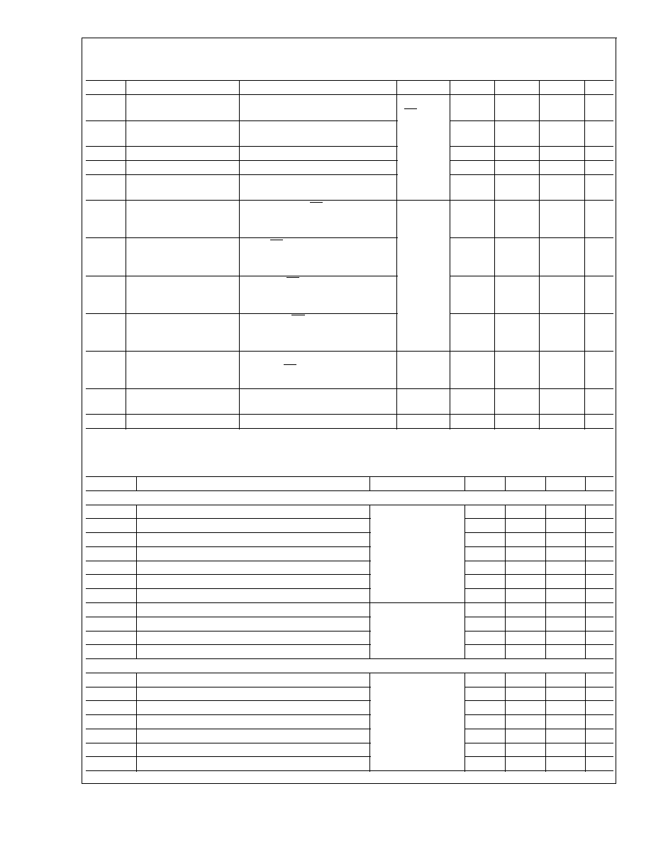
DC Electrical Characteristics
(Continued)
Over recommended operating supply voltage and temperature ranges unless otherwise specified (Notes 2, 3)
Symbol
Parameter
Conditions
Pin
Min
Typ
Max
Units
V
IH
Minimum Input High
Voltage
D
IN
, DE,
RE
2.0
V
CC
V
V
IL
Maximum Input Low
Voltage
GND
0.8
V
I
IH
Input High Current
V
IN
= V
CC
or 2.4V
-20
±
10
+20
µA
I
IL
Input Low Current
V
IN
= GND or 0.4V
-20
±
10
+20
µA
V
CL
Input Diode Clamp
Voltage
I
CLAMP
= -18 mA
-1.5
-0.8
V
I
CCD
Power Supply Current
Drivers Enabled,
Receivers Disabled
No Load, DE = RE = V
CC
,
DIN = V
CC
or GND
V
CC
55
80
mA
I
CCR
Power Supply Current
Drivers Disabled,
Receivers Enabled
DE = RE = 0V, V
ID
=
±
300mV
73
80
mA
I
CCZ
Power Supply Current,
Drivers and Receivers
TRI-STATE
Æ
DE = 0V; RE = V
CC
,
DIN = V
CC
or GND
35
80
mA
I
CC
Power Supply Current,
Drivers and Receivers
Enabled
DE = V
CC
; RE = 0V,
DIN = V
CC
or GND,
R
L
= 27
170
210
mA
I
OFF
Power Off Leakage
Current
V
CC
= 0V or OPEN,
D
IN
, DE, RE = 0V or OPEN,
V
APPLIED
= 3.6V (Port Pins)
DO+/RI+,
DO-/RI-
-20
+20
µA
C
OUTPUT
Capacitance
@
Bus Pins
DO+/RI+,
DO-/RI-
5
pF
c
OUTPUT
Capacitance
@
R
OUT
R
OUT
7
pF
AC Electrical Characteristics
Over recommended operating supply voltage and temperature ranges unless otherwise specified (Note 6)
Symbol
Parameter
Conditions
Min
Typ
Max
Units
DIFFERENTIAL DRIVER TIMING REQUIREMENTS
t
PHLD
Differential Prop. Delay High to Low (Note 8)
R
L
= 27
,
Figures 2, 3,
C
L
= 10 pF
0.6
1.4
2.2
ns
t
PLHD
Differential Prop. Delay Low to High (Note 8)
0.6
1.4
2.2
ns
t
SKD1
Differential Skew |t
PHLD
≠t
PLHD
| (Note 9)
80
ps
t
SKD2
Chip to Chip Skew (Note 12)
1.6
ns
t
SKD3
Channel to Channel Skew (Note 13)
0.25
0.45
ns
t
TLH
Transition Time Low to High
0.6
1.2
ns
t
THL
Transition Time High to Low
0.5
1.2
ns
t
PHZ
Disable Time High to Z
R
L
= 27
,
Figures 4, 5,
C
L
= 10 pF
3
8
ns
t
PLZ
Disable Time Low to Z
3
8
ns
t
PZH
Enable Time Z to High
3
8
ns
t
PZL
Enable Time Z to Low
3
8
ns
DIFFERENTIAL RECEIVER TIMING REQUIREMENTS
t
PHLD
Differential Prop. Delay High to Low (Note 8)
Figures 6, 7,
C
L
= 35 pF
1.6
2.4
3.2
ns
t
PLHD
Differential Prop Delay Low to High (Note 8)
1.6
2.4
3.2
ns
t
SDK1
Differential Skew |t
PHLD
≠t
PLHD
| (Note 9)
80
ps
t
SDK2
Chip to Chip Skew (Note 12)
1.6
ns
t
SDK3
Channel to Channel Skew (Note 13)
0.35
0.60
ns
t
TLH
Transition Time Low to High
1.5
2.5
ns
t
THL
Transition Time High to Low
1.5
2.5
ns
DS92L
V090A
www.national.com
4
AC Electrical Characteristics
(Continued)
Over recommended operating supply voltage and temperature ranges unless otherwise specified (Note 6)
Symbol
Parameter
Conditions
Min
Typ
Max
Units
DIFFERENTIAL RECEIVER TIMING REQUIREMENTS
t
PHZ
Disable Time High to Z
R
L
= 500
,
Figures 8, 9,
C
L
= 35 pF
4.5
10
ns
t
PLZ
Disable Time Low to Z
3.5
8
ns
t
PZH
Enable Time Z to High
3.5
8
ns
t
PZL
Enable Time Z to Low
3.5
8
ns
Note 1: "Absolute Maximum Ratings" are those values beyond which the safety of the device cannot be guaranteed. They are not meant to imply that the devices
should be operated at these limits. The table of "Electrical Characteristics" provides conditions for actual device operation.
Note 2: All currents into device pins are positive; all currents out of device pins are negative. All voltages are referenced to ground unless otherwise specified except
V
OD
,
V
OD
and V
ID
.
Note 3: All typicals are given for V
CC
= +3.3V and T
A
= +25∞C, unless otherwise stated.
Note 4: ESD Rating: HBM (1.5 k
, 100 pF)
>
4.5 kV EIAJ (0
, 200 pF)
>
300V.
Note 5: C
L
includes probe and fixture capacitance.
Note 6: Generator waveforms for all tests unless otherwise specified: f = 25 MHz, Z
O
= 50
, t
r
, t
f
=
<
1.0 ns (0%≠100%). To ensure fastest propagation delay and
minimum skew, data input edge rates should be equal to or faster than 1ns/V; control signals equal to or faster than 3ns/V. In general, the faster the input edge rate,
the better the AC performance.
Note 7: The DS92LV090A functions within datasheet specification when a resistive load is applied to the driver outputs.
Note 8: Propagation delays are guaranteed by design and characterization.
Note 9: t
SKD1
|t
PHLD
≠t
PLHD
| is the worse case skew between any channel and any device over recommended operation conditions.
Note 10: Only one output at a time should be shorted, do not exceed maximum package power dissipation capacity.
Note 11: V
OH
failsafe terminated test performed with 27
connected between RI+ and RI- inputs. No external voltage is applied.
Note 12: Chip to Chip skew is the difference in differential propagation delay between any channels of any devices, either edge.
Note 13: Channel to Channel skew is the difference in driver output or receiver output propagation delay between any channels within a device, either edge.
Applications Information
General application guidelines and hints may be found in the
following application notes: AN-808, AN-903, AN-971,
AN-977, and AN-1108.
There are a few common practices which should be implied
when designing PCB for Bus LVDS signaling. Recom-
mended practices are:
∑
Use at least 4 PCB board layer (Bus LVDS signals,
ground, power and TTL signals).
∑
Keep drivers and receivers as close to the (Bus LVDS
port side) connector as possible.
∑
Bypass each Bus LVDS device and also use distributed
bulk capacitance between power planes. Surface mount
capacitors placed close to power and ground pins work
best. Two or three high frequency, multi-layer ceramic
(MLC) surface mount (0.1 µF, 0.01 µF, 0.001 µF) in
parallel should be used between each V
CC
and ground.
The capacitors should be as close as possible to the V
CC
pin.
Multiple vias should be used to connect V
CC
and Ground
planes to the pads of the by-pass capacitors.
In addition, randomly distributed by-pass capacitors
should be used.
∑
Use the termination resistor which best matches the dif-
ferential impedance of your transmission line.
∑
Leave unused Bus LVDS receiver inputs open (floating).
Limit traces on unused inputs to
<
0.5 inches.
∑
Isolate TTL signals from Bus LVDS signals
MEDIA (CONNECTOR or BACKPLANE) SELECTION:
∑
Use controlled impedance media. The backplane and
connectors should have a matched differential imped-
ance.
TABLE 1. Functional Table
MODE SELECTED
DE
RE
DRIVER MODE
H
H
RECEIVER MODE
L
L
TRI-STATE MODE
L
H
LOOP BACK MODE
H
L
TABLE 2. Transmitter Mode
INPUTS
OUTPUTS
DE
D
IN
DO+
DO-
H
L
L
H
H
H
H
L
H
0.8V
<
D
IN
<
2.0V
X
X
L
X
Z
Z
TABLE 3. Receiver Mode
INPUTS
OUTPUT
RE
(RI+) ≠ (RI-)
L
L (
<
-100 mV)
L
L
H (
>
+100 mV)
H
L
-100 mV
<
V
ID
<
+100 mV
X
H
X
Z
X = High or Low logic state
L = Low state
Z = High impedance state
H = High state
DS92L
V090A
www.national.com
5