DS9637A
Dual Differential Line Receiver
General Description
The DS9637A is a Schottky dual differential line receiver
which has been specifically designed to satisfy the require-
ments of EIA Standards RS-422 and RS-423. In addition, the
DS9637A satisfies the requirements of MIL-STD 188-114
and is compatible with the International Standard CCITT rec-
ommendations. The DS9637A is suitable for use as a line re-
ceiver in digital data systems, using either single ended or
differential, unipolar or bipolar transmission. It requires a
single 5V power supply and has Schottky TTL compatible
outputs. The DS9637A has an operational input common
mode range of
±
7V either differentially or to ground.
Features
n
Dual channel
n
Single 5V supply
n
Satisfies EIA standards RS-422 and RS423
n
Built-in
±
35 mV hysteresis
n
High input common mode voltage range
n
High input impedance
n
TTL compatible outputs
n
Schottky technology
n
Extended temperature range
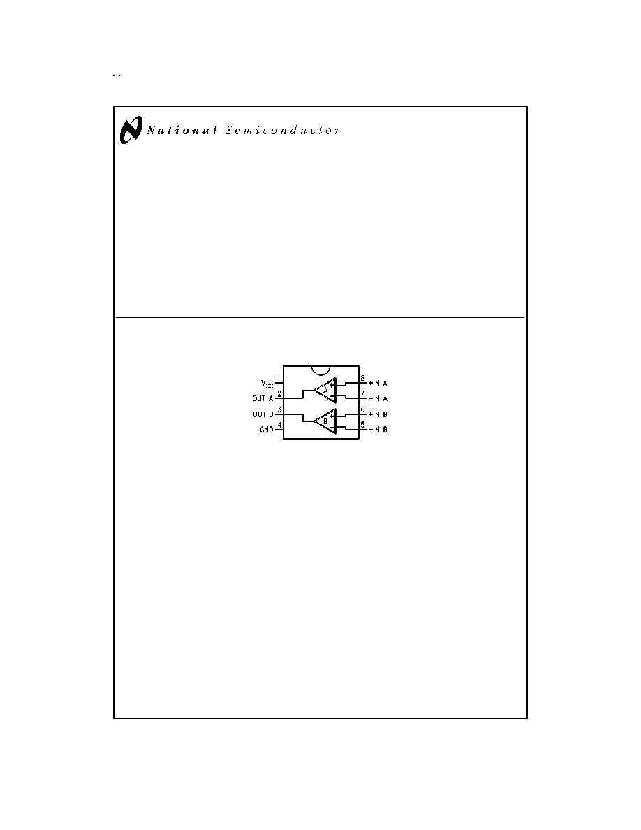
Connection Diagram
8≠Lead DIP and SO-8 Package
DS009621-1
Top View
Order Number DS9637ACM or DS9637ACN
See NS Package Number M08A or N08E
For Complete Military Product Specifications,
refer to the appropriate SMD or MDS.
Order Number DS9637AMJ/883
See NS Package Number J08A
May 1998
DS9637A
Dual
Differential
Line
Receiver
© 1998 National Semiconductor Corporation
DS009621
www.national.com
Absolute Maximum Ratings
(Note 2)
If Military/Aerospace specified devices are required,
please contact the National Semiconductor Sales Office/
Distributors for availability and specifications.
Storage Temperature Range
Ceramic DIP
-65∞C to + 175∞C
Molded DIP
-65∞C to + 150∞C
Lead Temperature
Ceramic DIP
(Soldering, 30 seconds)
300∞C
Molded DIP and SO Package
(Soldering, 10 seconds)
265∞C
Maximum Power Dissipation (Note 1) at 25∞C
Cavity Package
1300 mW
Molded Package
930 mW
SO Package
810 mW
V
CC
Lead Potential to Ground
-0.5V to 7.0V
Input Potential to Ground
±
15V
Differential Input Voltage
±
15V
Output Potential to Ground
-0.5V to +5.5V
Output Sink Current
50 mA
Recommended Operating
Conditions
DS9637AM
Min
Max
Units
Supply Voltage (V
CC
)
4.5
5.5
V
Operating Temperature (T
A
)
-55
+125
∞C
DS9637AC
Supply Voltage (V
CC
)
4.75
5.25
V
Operating Temperature (T
A
)
0
+70
∞C
Note 1: Derate cavity package 8.7 mW/∞C above 25∞C; derate molded DIP
package 7.5 mW/∞C above 25∞C; derate SO package 6.5 mW/∞C above 25∞C.
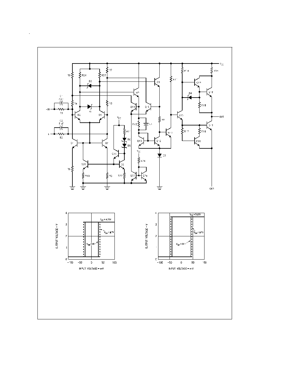
Electrical Characteristics
(Notes 3, 4)
Over recommended operating temperature and supply voltage ranges, unless otherwise specified
Symbol
Parameter
Conditions
Min
Typ
Max
Units
V
TH
Differential Input
-7.0V
V
CM
+7.0V
-0.2
+0.2
V
Threshold Voltage (Note 6)
V
TH(R)
Differential Input
-7.0V
V
CM
+7.0V
-0.4
+0.4
V
Threshold Voltage (Note 7)
I
I
Input Current
V
I
= 10V, 0V
V
CC
+5.5V
1.1
3.25
mA
(Note 8)
V
I
= -10V, 0V
V
CC
+5.5V
-1.6
-3.25
V
OL
Output Voltage LOW
I
OL
= 20 mA, V
CC
= Min
0.35
0.5
V
V
OH
Output Voltage HIGH
I
OH
= -1.0 mA, V
CC
= Min
2.5
3.5
V
I
OS
Output Short Circuit
V
O
= 0V, V
CC
= Max
-40
-75
-100
mA
Current (Note 5)
I
CC
Supply Current
V
CC
= Max, V
I
+ = 0.5V,
35
50
mA
V
I
- = GND
V
HYST
Input Hysteresis
V
CM
=
±
7.0V (See Curves)
70
mV
Note 2: "Absolute Maximum Ratings" are those values beyond which the safety of the device cannot be guaranteed. They are not meant to imply that the devices
should be operated at these limits. The tables of "Electrical Characteristics" provide conditions for actual device operation.
Note 3: Unless otherwise specified Min/Max limits apply across the -55∞C to +125∞C temperature range for DS9637AM and across the 0∞C to +70∞C range for the
DS9637ASC. All typicals are given for V
CC
= 5V and T
A
= 25∞C.
Note 4: All currents into the device pins are positive; all currents out of the device pins are negative. All voltages are referenced to ground unless otherwise specified.
Note 5: Only one output at a time should be shorted.
Note 6: V
DIFF
(Differential Input Voltage) = (V
I
+) - (V
I
-). V
CM
(Common Mode Input Voltage) = V
I
+ or V
I
-.
Note 7: 500
±
1% in series with inputs.
Note 8: The input not under test is tied to ground.
Switching Characteristics
V
CC
= 5.0V, T
A
= 25∞C
Symbol
Parameter
Conditions
Min
Typ
Max
Units
t
PLH
Propagation Delay Time
See AC Test Circuit
15
25
ns
Low to High
t
PHL
Propagation Delay Time
See AC Test Circuit
13
25
ns
High to Low
www.national.com
2

AC Test Circuit and Waveforms
Typical Applications
DS009621-5
Notes:
C
L
includes jig and probe capacitance.
All diodes are FD700 or equivalent.
FIGURE 2.
DS009621-6
V
I
Amplitude: 1.0V
Offset: 0.5V
Pulse Width: 100 ns
PRR: 5.0 MHz
t
r
= t
f
5.0 ns
FIGURE 3.
DS009621-7
Notes:
R
T
50
for RS-422 operation.
R
T
combined with input impedance of receivers must be greater than 90
.
FIGURE 4. RS-422 System Application (FIPS 1020) Differential Simplex Bus Transmission
www.national.com
4
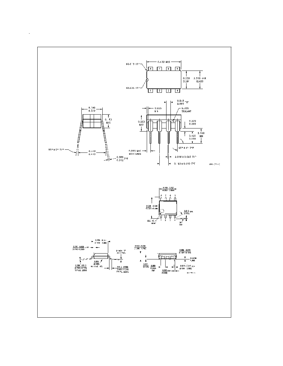
Physical Dimensions
inches (millimeters) unless otherwise noted
Ceramic Dual-In-Line Package (J)
Order Number DS9637AMJ/883
NS Package Number J08A
Molded Surface Mount Package (M)
Order Number DS9637ACM
NS Package Number M08A
www.national.com
5