
DS9638
RS-422 Dual High Speed Differential Line Driver
General Description
The DS9638 is a Schottky, TTL compatible, dual differential
line driver designed specifically to meet the EIA Standard
RS-422 specifications. It is designed to provide unipolar dif-
ferential drive to twisted pair or parallel wire transmission
lines. The inputs are TTL compatible. The outputs are similar
to totem pole TTL outputs, with active pull-up and pull-down.
The device features a short circuit protected active pull-up
with low output impedance and is specified to drive 50
transmission lines at high speed. The mini-DIP provides high
package density.
Features
n
Single 5V supply
n
Schottky technology
n
TTL and CMOS compatible inputs
n
Output short circuit protection
n
Input clamp diodes
n
Complementary outputs
n
Minimum output skew (
<
1.0 ns typical)
n
50 mA output drive capability for 50
transmission lines
n
Meets EIA RS-422 specifications
n
Propagation delay of less than 10 ns
n
"Glitchless" differential output
n
Delay time stable with V
CC
and temperature variations
(
<
2.0 ns typical) (
Figure 3)
n
Extended temperature range
Connection Diagram
8-Lead DIP
DS009622-1
Top View
Order Number DS9638CM or DS9638CN
See NS Package Number M08A or N08E
For Complete Military Product Specifications,
refer to the appropriate SMD or MDS.
Order Number DS9638MJ/883
See NS Package Number J08A
May 1998
DS9638
RS-422
Dual
High
Speed
Differential
Line
Driver
� 1998 National Semiconductor Corporation
DS009622
www.national.com
Absolute Maximum Ratings
(Note 2)
If Military/Aerospace specified devices are required,
please contact the National Semiconductor Sales Office/
Distributors for availability and specifications.
Storage Temperature Range
Ceramic DIP
-65�C to +175�C
Molded DIP and SO-8
-65�C to +150�C
Lead Temperature
Ceramic DIP (Soldering, 60 sec.)
300�C
Molded DIP (Soldering, 10 sec.)
265�C
Maximum Power Dissipation (Note 1) at 25�C
Cavity Package
1300 mW
Molded Package
930 mW
SO Package
810 mW
V
CC
Lead Potential to Ground
-5V to 7V
Input Voltage
-0.5V to +7V
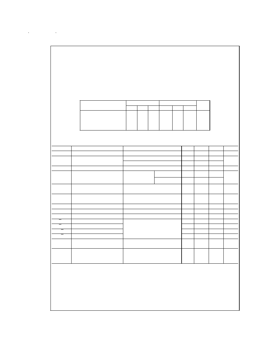
Recommended Operating Conditions
DS9638M
DS9638C
Min
Typ
Max
Min
Typ
Max
Units
Supply Voltage (V
CC
)
4.5
5.0
5.5
4.75
5.0
5.25
V
Output Current HIGH (I
OH
)
-50
-50
mA
Output Current LOW (I
OL
)
50
40
50
mA
Operating Temperature (T
A
)
-55
25
125
0
25
70
�C
Note 1: Derate cavity package 8.7 mW/�C above 25�C; derate molded DIP package 7.5 mW/�C above 25�C; derate SO package 6.5 mW�C above 25�C.
Electrical Characteristics
(Notes 3, 4)
Over recommended operating temperature and supply voltage ranges, unless otherwise specified
Symbol
Parameter
Conditions
Min
Typ
Max
Units
V
IH
Input Voltage HIGH
2.0
V
V
IL
Input Voltage LOW
0�C to +70�C
0.8
V
-55�C to +125�C
0.5
V
IC
Input Clamp Voltage
V
CC
= Min, I
I
= -18 mA
-1.0
-1.2
V
V
OH
Output Voltage HIGH
V
CC
= Min,
V
IH
= V
IH Min
,
V
IL
= V
IL Max
I
OH
= -10 mA
2.5
3.5
V
I
OH
= -40 mA
2.0
V
OL
Output Voltage LOW
V
CC
= Min, V
IH
= V
IH Min
,
0.5
V
V
IL
= V
IL Max
, I
OL
= 40 mA
I
I
Input Current at Maximum
V
CC
= Max, V
I Max
= 5.5V
50
�A
Input Voltage
I
IH
Input Current HIGH
V
CC
= Max, V
IH
= 2.7V
25
�A
I
IL
Input Current LOW
V
CC
= Max, V
IL
= 0.5V
-200
�A
I
OS
Output Short Circuit Current
V
CC
= Max, V
O
= 0V (Note 4)
-50
-150
mA
V
T
, V
T
Terminated Output Voltage
See
Figure 1
2.0
V
V
T
�V
T
Output Balance
0.4
V
V
OS
, V
OS
Output Offset Voltage
3.0
V
V
OS
�V
OS
Output Offset Balance
0.4
V
I
X
Output Leakage Current
T
A
= 25�C
100
�A
-0.25V
<
V
X
<
5.5V
I
CC
Supply Current
V
CC
= 5.5V,
(Both Drivers)
All input at 0V,
45
65
mA
No Load
Note 2: "Absolute Maximum Ratings" are those values beyond which the safety of the device cannot be guaranteed. They are not meant to imply that the devices
should be operated at these limits. The tables of "Electrical Characteristics provide conditions for actual device operation.
Note 3: Unless otherwise specified min/max limits apply across the -55�C to +125�C temperature range for the DS9638M and across the 0�C to +70�C range for
the DS9638C. All typicals are given for V
CC
= 5V and T
A
= 25�C.
Note 4: All currents into the device pins are positive; all currents out of the device pins are negative. All voltages are referenced to ground unless otherwise specified.
Note 5: Only one output at a time should be shorted.
www.national.com
2
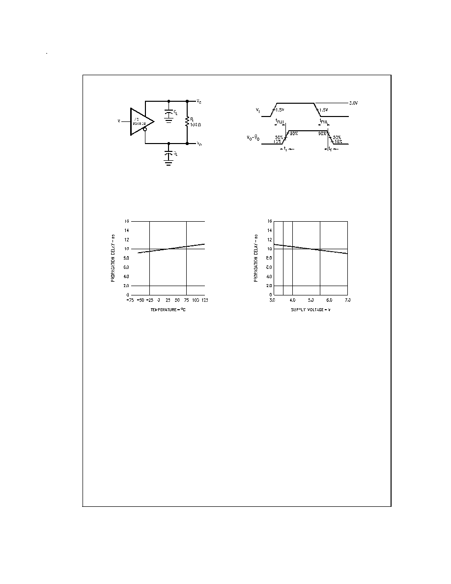
Switching Characteristics
V
CC
= 5.0V, T
A
= 25�C.
Symbol
Parameter
Conditions
Min
Typ
Max
Units
t
PHL
Propagation Delay
C
L
= 15 pF
10
20
ns
t
PLH
R
L
= 100
, See
Figure 2
10
20
ns
t
f
Fall Time, 90%�10%
10
20
ns
t
r
Rise Time, 10%�90%
10
20
ns
t
PO
�t
PO
Skew Between Outputs
1.0
ns
A/A and B/B
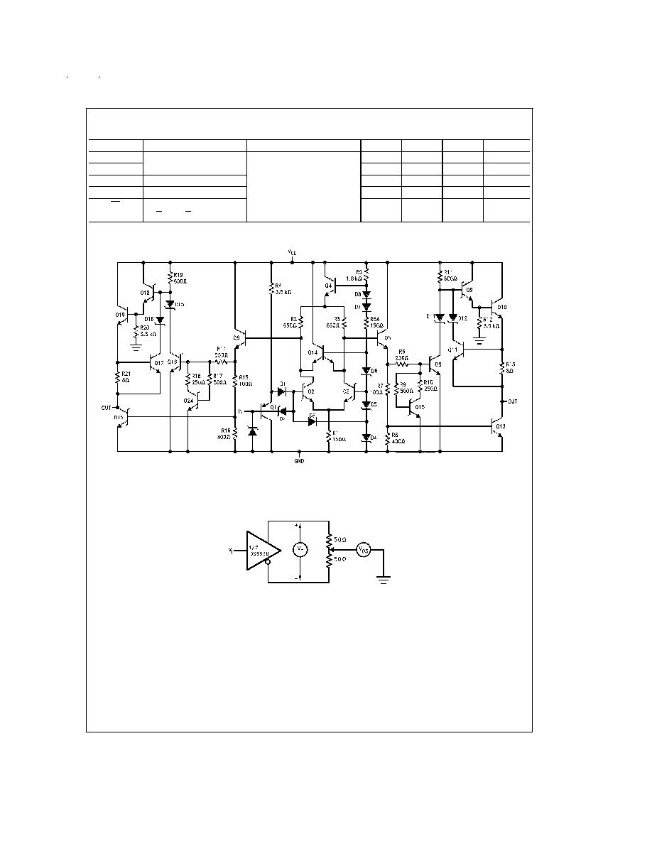
DC Test Circuit
DS009622-2
FIGURE 1. Equivalent Circuit
DS009622-3
FIGURE 2. Terminated Output Voltage and Output Balance
www.national.com
3
DC Test Circuit
(Continued)
DS009622-4
Note 6: The pulse generator has the following characteristics:
C
L
includes probe and jig capacitance.
PRR = 500 kHz, t
W
= 100 ns,
t
r
5.0 ns, Z
O
= 50
.
DS009622-5
FIGURE 3. AC Test Circuit and Voltage Waveform
DS009622-6
DS009622-7
FIGURE 4. Typical Delay Characteristics
www.national.com
4
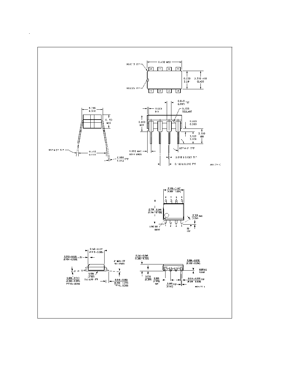
Physical Dimensions
inches (millimeters) unless otherwise noted
Ceramic Dual-In-Line Package (J)
Order Number DS9638MJ/883
NS Package Number J08A
Ceramic Dual-In-Line Package (M)
Order Number DS9638CM
NS Package Number M08A
www.national.com
5