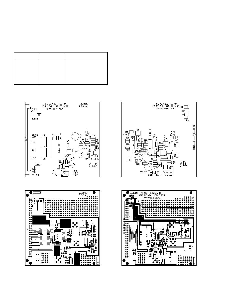
Description
The Comlinear E949PCASM Evaluation board is
designed to support simple and effective evaluation of
the CLC949 Analog-to-Digital Converter. To operate the
converter you need only supply power, a clock and a
signal to be digitized. The evaluation board uses a
common Eurocard connector to make the power, ground
and data connections with the rest of the evaluation
system. Options exist on the board to use an amplifier
based input to the converter, a transformer coupled input,
or direct input, as well as options to generate a clock from
a sinusoidal source or to use a suitable CMOS clock.
The bias points for the converter can be selected via a
DIP switch. For a complete description of these various
options, please refer to the CLC949 datasheet.
Default Configuration
The CLC949 Evaluation board is shipped configured for
options 2 and 4 (DC coupled input using amplifiers,
CMOS clock generator enabled). The output data format
is offset binary and the bias point is selected to be 200µA,
allowing 20MHz operation.
Clock Generation
The evaluation circuitry includes a clock generation
circuit that will convert a sinusoidal input to a CMOS
clock for use by the CLC949. When using this option, the
clock signal that is provided should be 2-3V
pp
(10-
14dBm). For best results when digitizing high speed
input signals, the converter must have a very low jitter
clock. To generate this the sinusoidal input must have
very low phase noise. In a laboratory environment,
Comlinear suggests the use of a low phase noise
synthesizer such as the HP8662 or the HP8643 as a
clock source.
There is also an option that will enable you to provide a
TTL or CMOS clock directly to the board. The clock is
provided through an SMA connector, regardless of the
clocking option chosen. To enable the input of
a digital clock, remove the three jumpers labeled
OPT4
and insert a jumper at the point labeled
OPT1-3. These
jumpers can be found on the opposite side of the board
to the CLC949 and a surface mount 0
resistors.
Analog Input Conditioning
The CLC949 requires a differential input signal,
centered around a bias point of approximately 2.25V The
evaluation board offers three options for providing this
input:
s
Option 1 uses a transformer to phase split the
input signal and to provide the appropriate
offset voltage. This option will result in the
lowest distortion signal for input frequencies of
1MHz or higher. Since the transformer is not
able to pass frequencies lower than about
50kHz, this option is not a good choice if your
signal must be DC coupled. If you want to use
this option, install the transformer and the two
jumpers labeled
OPT1, and remove the three
jumpers labeled
OPT2. All of these jumpers
can be found on the back side of the board.
The transformer shipped with the board is a 1:1
transformer, therefore the input to it should be
2V
pp
in order to obtain a full scale output.
s
Option 2 uses an amplifier based circuit to
perform the phase splitting and DC offset. This
circuit is described in more detail in the
CLC949 datasheet. Option 2 is the default
condition in which the board is shipped. Using
this option, a 2V
pp
signal, with no DC offset
is applied to the input SMA to obtain a full
scale output.
s
Option 3 requires that you provide a differential
input signal with the proper offsets to the SMA
connectors labeled
+VIN and -VIN. To enable
this option, remove the three jumpers labeled
OPT2 and install the jumpers labeled OPT3.
DATA and Clock Outputs
The CLC949 Evaluation board is equipped with 74F574
latched which latch the CLC949 output data and drive the
Eurocard connector. An inverted version of the A/D clock
is also provided on the Eurocard connector. The output
data format of the CLC949 is selectable between Offset
Binary or Twos Complement via the Jumper
OPT6. For
Offset binary operation install the jumper in the location
OPT6A, two's complement is achieved by use of OPT6B.
These jumpers can be found on the front of the board,
just above the CLC949 chip.
CLC949 Evaluation Board
Part Number E949PCASM
August 1996
N
© 1996 National Semiconductor Corporation
http://www.national.com
Printed in the U.S.A.

http://www.national.com
6
Lit #660949-001
Customer Design Applications Support
National Semiconductor is committed to design excellence. For sales, literature and technical support, call the
National Semiconductor Customer Response Group at 1-800-272-9959 or fax 1-800-737-7018.
Life Support Policy
National's products are not authorized for use as critical components in life support devices or systems without the express written approval of the
president of National Semiconductor Corporation. As used herein:
1. Life support devices or systems are devices or systems which, a) are intended for surgical implant into the body, or b) support or
sustain life, and whose failure to perform, when properly used in accordance with instructions for use provided in the labeling, can
be reasonably expected to result in a significant injury to the user.
2. A critical component is any component of a life support device or system whose failure to perform can be reasonably expected to
cause the failure of the life support device or system, or to affect its safety or effectiveness.
National Semiconductor
National Semiconductor
National Semiconductor
National Semiconductor
Corporation
Europe
Hong Kong Ltd.
Japan Ltd.
1111 West Bardin Road
Fax: (+49) 0-180-530 85 86
13th Floor, Straight Block
Tel: 81-043-299-2309
Arlington, TX 76017
E-mail: europe.support.nsc.com
Ocean Centre, 5 Canton Road
Fax: 81-043-299-2408
Tel: 1(800) 272-9959
Deutsch Tel: (+49) 0-180-530 85 85
Tsimshatsui, Kowloon
Fax: 1(800) 737-7018
English Tel: (+49) 0-180-532 78 32
Hong Kong
Francais Tel: (+49) 0-180-532 93 58
Tel: (852) 2737-1600
Italiano Tel: (+49) 0-180-534 16 80
Fax: (852) 2736-9960
National does not assume any responsibility for use of any circuitry described, no circuit patent licenses are implied and National reserves the right at any time without notice to change said
circuitry and specifications.
N