 | –≠–ª–µ–∫—Ç—Ä–æ–Ω–Ω—ã–π –∫–æ–º–ø–æ–Ω–µ–Ω—Ç: EM6605 | –°–∫–∞—á–∞—Ç—å:  PDF PDF  ZIP ZIP |

(0 0,&52(/(&7521,&0$5,1 6$
© EM Microelectronic-Marin SA, 2/99, Rev. B/243
1
EM6605 - 4 bit
Microcontroller
Features
∑
Low
Power - typical 4.0µA active mode
- typical 2.5µA standby mode
- typical 0.3µA sleep mode
@ 1.8V, 32kHz, 25 ∞C
∑
Low Voltage - 1.8 to 5.5V
∑
RC oscillator 30 - 300kHz
∑
buzzer
- three tone
∑
ROM
-
2k
◊
16 (Mask Programmed)
∑
RAM
-
96
◊
4 (User Read/Write)
∑
2 clocks per instruction cycle
∑
RISC architecture
∑
4 software configurable 4-bit ports
∑
Up to 16 inputs
(4 ports)
∑
Up to 12 outputs
(3 ports)
∑
Serial (Output) Write buffer - SWB
∑
Voltage level detection
∑
Analogue
watchdog
∑
Timer
watchdog
∑
8 bit timer / event counter
∑
Internal interrupt sources (timer, event
counter, prescaler)
∑
External interrupt sources (portA + portC)
Description
The EM66XX series is an advanced single chip low
cost, mask programmed CMOS 4-bit microcontroller.
It contains ROM, RAM, watchdog timer, oscillation
detection circuit, combined timer / event counter,
prescaler, voltage level detector and a number of
clock functions. Its low voltage and low power
operation make it the most suitable controller for
battery, stand alone and mobile equipment. The
EM66XX series is manufactured using EM's
Advanced Low Power CMOS Process.
Typical Applications
∑
sensor interfaces
∑
domestic appliances
∑
security systems
∑
automotive
controls
∑
TV & audio remote controls
∑
measurement
equipment
∑
R/F and IR. control
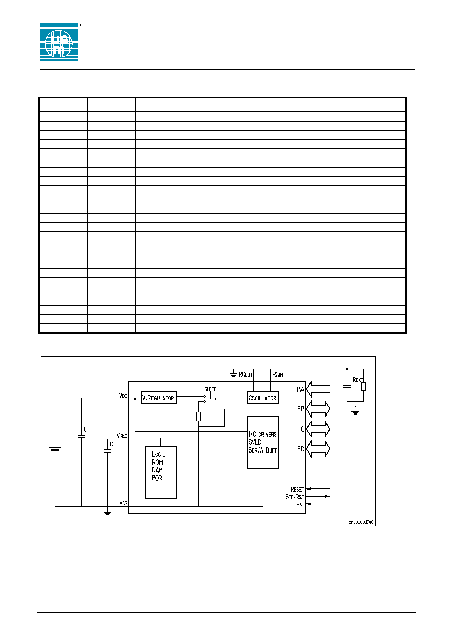
Figure 1.Architecture
Figure 2.Pin Configuration

EM6605
© EM Microelectronic-Marin SA, 02/99, Rev. B/243
2
EM6605 at a glance
∑
Power Supply
- Low Voltage, low power architecture
including internal voltage regulator
- 1.8V ... 5.5 V battery voltage
- 4.0
$ LQ DFWLYH PRGH
- 2.5
$ LQ VWDQGE\ PRGH
- 0.3
$ LQ VOHHS PRGH
@ 1.8V, 32kHz, 25 ∞C
- RC oscillator from 30-300kHz
∑
RAM
- 96 x 4 bit, direct addressable
∑
ROM
- 2048 x 16 bit metal mask programmable
∑
CPU
- 4 bit RISC architecture
- 2 clock cycles per instruction
- 72 basic instructions
∑
Main Operating Modes and Resets
- Active mode
(CPU is running)
- Standby mode
(CPU in Halt)
- Sleep mode
(No clock, Reset State)
- Initial reset on Power-On (POR)
- External reset pin
- Watchdog timer (time-out) reset
- Oscillation detection watchdog reset
- Reset with input combination on PortA
(metal option)
∑
Supply Voltage Level Detector
- 3 software selectable levels defined by user
between 1.9V and 4.5V)
- Busy flag during measure
- Active only on request during measurement to
reduce power consumption
∑
4-Bit Input PortA
- Direct input read
- Debounced or direct input selectable (reg.)
- Interrupt request on input's rising or falling edge,
selectable by register.
- Pull-down or none, selectable by met. mask
- Software test variables for conditional jumps
- PA3 input for the event counter
- Reset with input combination on PortA
(metal option)
∑
4-Bit Input/Output PortB
- separate input or output selection by register
- Pull-up, Pull-down or none, selectable by metal
mask if used as Input
- Buzzer output on PB0
∑
4-Bit Input/Output PortC
- Input or Output port as a whole port
- Debounced or direct input selectable (reg.)
- Interrupt request on input's rising or falling edge,
selectable by register.
- Pull-up, pull-down or none, selectable by
metal mask if used as input
- CMOS or N-channel open drain mode
∑
4-Bit Input/Output PortD
- Input or Output port as a whole port
- Pull-up, Pull-down or none, selectable by metal
mask if used as Input
- CMOS or N-channel open drain mode
- Serial Write Buffer clock and data output
∑
Serial (output) Write Buffer
- max. 256 bits long clocked with
ck[15]/ck[14]/ck[12]/ck[11] = 16/8/2/1kHz
- automatic send mode
- interactive send mode : interrupt request
when buffer is empty
∑
RCoscillator
- RC oscillator with an external resistor for
frequency adjustment in range from
30kHz to 300kHz
- Production tolerance
±
20%
- Temperature toll.
±
5%, -20
∞
C<T<70
∞
C
∑
Buzzer Output
- if used output on PB0
- 3 tone buzzer - 1kHz, 2kHz, 2.66kHz @32kHz
∑
Prescaler
-
15 stage system clock divider down to 1 Hz
- 3 interrupt requests : 1Hz/8Hz/32Hz
- Prescaler reset ck[14]-ck[1] (from 8kHz-1Hz)
∑
8-bit Timer / Event Counter
-
8-bit auto-reload count-down timer
- 6 different clocks from prescaler
- or event counter from the PA3 input
- parallel load
- interrupt request when comes to 00 hex.
∑
Interrupt Controller
-
4 external interrupt sources from PortA
- 3 internal interrupt sources, prescaler, timer and
Serial Write Buffer
- each interrupt request is individually maskable
- interrupt request flag is cleared automatically on
register read
NOTE: All frequencies on this page are related to 32.7kHz typical system clock

EM6605
© EM Microelectonic-Marin SA, 02/99, Rev. B/243
3
Table of Contents
1.
Operating modes................................................ 5
1.1.
STANDBY M
ODE
......................................... 5
1.2.
SLEEP M
ODE
............................................... 5
2.
Power Supply...................................................... 5
3.
Reset ................................................................... 6
3.1.
O
SCILLATION DETECTION CIRCUIT
................... 6
3.2.
R
ESET
P
IN
.................................................... 6
3.3.
I
NPUT PORT
(PA0..PA3) RESET ................... 7
3.4.
W
ATCHDOG
T
IMER
RESET............................ 7
3.5.
CPU S
TATE AFTER
RESET ........................... 7
4.
Oscillator............................................................. 8
4.1.
P
RESCALER
.................................................. 8
5.
Watchdog timer .................................................. 9
6.
INPUT and OUTPUT ports............................... 10
6.1.
P
ORT
A ....................................................... 10
6.2.
P
ORT
A
REGISTERS
...................................... 11
6.3.
P
ORT
B ....................................................... 12
6.4.
P
ORT
B
REGISTERS
...................................... 12
6.5.
P
ORT
C ....................................................... 13
6.6.
P
ORT
C
REGISTERS
...................................... 13
6.7.
P
ORT
D ....................................................... 15
6.8.
P
ORT
D
REGISTERS
...................................... 15
7.
BUZZER............................................................. 16
7.1.
B
UZZER
R
EGISTER
...................................... 16
8.
Timer/Event Counter ........................................ 17
8.1.
T
IMER
/C
OUNTER REGISTERS
........................ 18
9.
Interrupt Controller .......................................... 19
9.1.
I
NTERRUPT CONTROL REGISTERS
.................. 19
10.
Supply Voltage Level Detector (SVLD) ....... 21
10.1.
SVLD
REGISTER
..................................... 21
11.
Serial (Output) Write Buffer - SWB ............. 22
11.1.
SWB A
UTOMATIC SEND MODE
................. 24
11.2.
SWB I
NTERACTIVE SEND
MODE
............... 26
12.
STroBe / RESet Output ................................ 27
13.
Test at EM - Active Supply Current test...... 27
14.
Metal Mask Options ..................................... 27
15.
Peripheral memory map .............................. 29
16.
Measured Electrical Behaviors ................... 31
16.1.
IDD C
URRENT
........................................ 31
16.2.
F
REQUENCY
........................................... 32
16.3.
R
EGULATED
V
OLTAGE
............................. 32
16.4. O
UTPUT CURRENTS
................................. 33
16.5.
P
ULL
U
P
/ D
OWN
R
ESISTORS
................... 35
17.
Electrical specifications .............................. 36
17.1.
A
BSOLUTE MAXIMUM RATINGS
.................. 36
17.2.
S
TANDARD
O
PERATING
C
ONDITIONS
........ 36
17.3.
H
ANDLING
P
ROCEDURES
......................... 36
17.4.
DC
CHARACTERISTICS
- P
OWER
S
UPPLY
.. 36
17.5.
DC
CHARACTERISTICS
- I
N
/O
UT
P
INS
....... 37
17.6.
DC
CHARACTERISTICS
- S V D L
EVELS
.... 38
17.7.
RC O
SCILLATOR
..................................... 39
17.8.
I
NPUT
T
IMING CHARACTERISTICS
.............. 39
18.
Die: Pad Location Diagram ......................... 40
19.
Packages ...................................................... 41
20.
CHIP marking : ............................................. 43
20.1.
CUSTOMER
MARKING
: ......................... 43
21.
ORDERING information :............................. 43
21.1.
P
ACKAGED DEVICE ORDERING
.................. 43
21.2.
DIE
FORM
O
RDERING
.............................. 43
Table of Figures
Figure 1.Architecture..................................................... 1
Figure 2.Pin Configuration............................................. 1
Figure 3.Typical Configuration....................................... 4
Figure 4.Mode Transition diagram................................. 5
Figure 5.System reset generation ................................. 6
Figure 6.Port A............................................................ 11
Figure 7.Port B............................................................ 12
Figure 8.Port C............................................................ 14
Figure 9.Port D............................................................ 15
Figure 10.Timer / Event Counter ................................. 17
Figure 11.Interrupt Request generation ....................... 20
Figure 12.Serial write buffer ........................................ 23
Figure 13.Automatic Serial Write Buffer transmission . 24
Figure 14.Interactive Serial Write Buffer transmission. 26
Figure 15. EM6605 PAD Location Diagram................. 40
Figure 16. Dimensions of DIP24 Package ≠ "A" ......... 41
Figure 17. Dimensions of TSSOP24 Package ≠ "F" ... 42
Figure 18.Dimensions of SOIC24 Package ≠ "B" ....... 42
EM Microelectronic-Marin SA cannot assume responsibility for use of any circuitry described other than
circuitry entirely embodied in an EM Microelectronic-Marin SA product. EM Microelectronic-Marin SA
reserves the right to change the circuitry and specifications without notice at any time. You are strongly
urged to ensure that the information given has not been superseded by a more up-to-date version.
EM6605
© EM Microelectronic-Marin SA, 02/99, Rev. B/243
4
Table 1. Pin Description
Pin Number Pin Name
Function
Remarks
1
port A, 0
input 0 port A
interrupt request; tvar 1
2
port A, 1
input 1 port A
interrupt request; tvar 2
3
port A, 2
input 2 port A
interrupt request; tvar 3
4
port A, 3
input 3 port A
interrupt request; event counter input
5
port B, 0
input / output 0 port B
buzzer output
6
port B, 1
input / output 1 port B
7
port B, 2
input / output 2 port B
8
port B, 3
input / output 3 port B
9
test
test input terminal
for EM test purpose only
10*
RCin
RC external resistor
typically 120kOhm - 330kOhm
11
RCout/NC
RC output frequency
connect it at Vss - Ground
12
Vss
negative power supply terminal
13
STB/RST
strobe / reset status
µC reset state + port B, C, D, write
14
port C, 0
input / output 0 port C
interrupt request
15
port C, 1
input / output 1 port C
interrupt request
16
port C, 2
input / output 2 port C
interrupt request
17
port C, 3
input / output 3 port C
interrupt request
18
port D, 0
input / output 0 port D
SWB Serial Clock Output
19
port D, 1
input / output 1 port D
SWB Serial Data Output
20
port D, 2
input / output 2 port D
21
port D, 3
input / output 3 port D
22
reset
reset terminal
Active high (internal pull-down)
23
Vreg
internal voltage regulator
Needs typ. 100nF capacitor tw. Vss
24
Vdd
positive power supply terminal
Figure 3.Typical Configuration
∑
RCin node is hi impedance node and the connection towards Rext to fix the frequency
should be as short as possible. Treat this node as Quartz node.
For Vdd less then 2.0V it is recommended that Vdd is connected directly to Vreg
For Vdd>2.2V then the configuration shown in Fig.3 should be used.

EM6605
© EM Microelectonic-Marin SA, 02/99, Rev. B/243
5
1. Operating modes
The EM6605 has two low power dissipation modes:
STANDBY and SLEEP. Figure 4 is a transition diagram
for these modes.
1.1. STANDBY Mode
Executing a HALT instruction puts the EM6605 into
STANDBY mode. The voltage regulator, oscillator,
Watchdog timer, interrupts and timer/event counter are
operating. However, the CPU stops since the clock
related to instruction execution stops. Registers, RAM,
and I/O pins retain their states prior to STANDBY mode.
STANDBY is cancelled by a RESET or an Interrupt
request if enabled.
Table 2 : shows the state of the EM6605 functions in
STANDBY and SLEEP modes.
1.2. SLEEP Mode
Writing to the SLEEP bit in the IntRq register puts the
EM6605 in SLEEP mode. The oscillator stops and most
functions of the EM6605 are inactive. To be able to write
the SLEEP bit, the SLmask bit must first be set to 1. In
SLEEP mode only the voltage regulator and RESET
input are active. The RAM data integrity is maintained.
SLEEP mode may be cancelled only by a RESET at the
terminal pin of the EM6605. The RESET must be high
for at least 2µsec.
Figure 4.Mode Transition diagram
Table 2.StandBy and Sleep Activities
FUNCTION
STANDBY SLEEP
Oscillator
Active
Stopped
Instruction Execution Stopped
Stopped
Registers and Flags
Retained
Reset
Interrupt Functions
Active
Stopped
RAM
Retained
Retained
Timer/Counter
Active
Stopped
Watchdog
Active
Stopped
I/O pins
Active
High-Z or
Retained
Supply VLD
Stopped
Stopped
Reset pin
Active
Active
Due to the cold start characteristics of the oscillator, waking up from SLEEP mode may take some time to
guarantee that the oscillator has started correctly. During this time the circuit is in RESET and the strobe
output STB/RST is high. Waking up from SLEEP mode clears the SLEEP flag but not the SLmask bit. By
reading SLmask one can therefore determine if the EM6605 was powered up (SLmask = 0), or woken
from SLEEP mode (SLmask = 1).
2. Power Supply
The EM6605 is supplied by a single external power supply between Vdd and Vss, the circuit reference
being at Vss (ground). A built-in voltage regulator generates Vreg providing regulated voltage for the
oscillator and internal logic. Output drivers are supplied directly from the external supply Vdd. A typical
connection configuration is shown in Figure 3.
For Vdd less then 2.0V it is recommended that Vdd is connected directly to Vreg
For Vdd>2.2V then the configuration shown in Fig.3 should be used.