 | –≠–ª–µ–∫—Ç—Ä–æ–Ω–Ω—ã–π –∫–æ–º–ø–æ–Ω–µ–Ω—Ç: EQ50F100 | –°–∫–∞—á–∞—Ç—å:  PDF PDF  ZIP ZIP |
EQ50F100
1Gbps - 6.25 Gbps Backplane Equalizer
General Description
The EQ50F100 is a equalizer designed to compensate
transmission medium losses and reduce the medium-
induced deterministic jitter. It is optimized for operation from
1Gbps to 6.25Gbps, on printed circuit backplane for up to
30" of FR4 striplines with backplane connectors at both
ends. It is code independent, and functioning equally well for
short run length, balanced codes such as 8b/10b, commonly
used in multiplexed 1.25 Gbps Ethernet Systems.
The equalizer uses differential CML inputs and outputs with
feed-through pin-outs, mounted in a 3 mm x 3 mm 6≠pin
leadless LLP package. It is powered from single 1.8V supply
and consumes 85 mW.
Features
n
Recovers 6.25 Gbps signals after 30" of FR4
n
Single 1.8V power supply
n
Low power consumption: 85mW
n
Equalize up to 20dB loss at 2.5 GHz
n
35 ps residual deterministic jitter at 5 Gbps
n
On-chip CML terminations
n
Small 3 mm x 3 mm 6≠pin leadless LLP package
Simplified Function Diagram
20096801
Note: Information contained in this datasheet is subject to change due to changes in design, specification and/or process, before EQ50F100 is production
released.
April 2005
EQ50F100
1Gbps
-
6.25
Gbps
Backplane
Equalizer
© 2005 National Semiconductor Corporation
DS200968
www.national.com

Simplified Block Diagram
20096802
Pin Descriptions
Pin Name
Pin
Number
I/O, Type
Description
HIGH SPEED DIFFERENTIAL I/O
IN-
IN+
1
6
I, CML
Inverting and non-inverting CML differential inputs to the equalizer. An on-chip 100
terminating resistor is connected between IN+ and IN-.
OUT-
OUT+
3
4
O, CML
Inverting and non-inverting CML differential outputs from the equalizer. An on-chip
50
terminating resistor connects OUT+ to V
DD
and OUT- to V
DD
.
POWER
V
DD
5
I, Power
V
DD
= 1.8V
±
5%. V
DD
pins should be tied to V
DD
plane through low inductance
path. A 0.01 µF bypass capacitor should be connected between the V
DD
pin and the
GND planes.
GND
2
I, Power
Ground reference. GND should be tied to a solid ground plane through a low
impedance path.
Exposed
Pad
PAD
I, Power
Connect to GND. The exposed pad at the center of the package should be
connected to ground plane of the board to enhance thermal and electrical
performance of the package.
Note: I = Input
O = Output
Pin Diagram
20096803
Top View Shown
3 mm x 3 mm 6-Pin LLP Package
EQ50F100
www.national.com
2

Absolute Maximum Ratings
(Note 1)
If Military/Aerospace specified devices are required,
please contact the National Semiconductor Sales Office/
Distributors for availability and specifications.
Supply Voltage (V
DD
)
-0.3V to +2.5V
CML Input/Output Voltage
-0.3V to (V
DD
+ 0.3V)
Junction Temperature
+150∞C
Storage Temperature
-65∞C to +150∞C
Lead Temp. (Soldering, 5 sec.)
+260∞C
ESD Rating
HBM, 1.5 k
, 100 pF
EIAJ, 0
, 200 pF
>
7 kV
>
200V
Thermal Resistance
JA
, No Airflow
54∞C/W
Recommended Operating
Conditions
Min
Typ
Max
Units
Supply Voltage
(V
DD
to GND)
1.71
1.8
1.89
V
Ambient Temperature
-40
25
85
∞C
Electrical Characteristics
Over recommended operating supply and temperature ranges unless other specified.
Symbol
Parameter
Conditions
Min
Typ
(Note 2)
Max
Units
POWER
P
Power Supply Consumption
85
106
mW
N
Supply Noise Tolerance (Note 3) 10 Hz≠100 Hz
100 Hz≠10 MHz
10 MHz≠2.5 GHz
100
50
10
mV
P-P
mV
P-P
mV
P-P
CML RECEIVER INPUTS (IN+, IN-)
V
IN
Input Voltage Swing
Differential signal to equalizer,
measured before test channel
400
1600
mV
P-P
R
LI
Differential Input Return Loss
100 MHz≠2.5 GHz, with fixture's
effect de-embedded
15
dB
R
IN
Input Resistance
Differential across IN+ and IN-
85
100
115
CML OUTPUTS (OUT+, OUT-)
V
O
Output Voltage Swing
Measured differentially with
OUT+ and OUT- terminated by
50
to GND through DC
block(Notes 9, 11)
450
800
mV
P-P
t
R
, t
F
Transition Time
20% to 80% of differential output
voltage, measured with 1" from
output pins. (Notes 9, 11)
30
45
60
ps
R
O
Output Resistance
Single-ended to V
DD
42
50
58
R
LO
Differential Output Return Loss
100 MHz≠2.5 GHz, with fixture's
effect de-embedded. IN+ = static
high.
14
dB
EQUALIZATION
DJ1
Residual Deterministic Jitter at
6.25 Gb/s
Multiplexed K28.5 pattern,
(Notes 4, 8), 30" Test channel,
V
IN
= 1V
P-P
. (Note 11)
0.25
0.4
UI
P-P
DJ2
Residual Deterministic Jitter at
5 Gb/s
Multiplexed K28.5 pattern,
(Notes 5, 8), 30" Test channel.
V
IN
= 1V
P-P
. (Note 11)
0.13
0.35
UI
P-P
DJ3
Residual Deterministic Jitter at
2.5 Gb/s
Multiplexed K28.5 pattern,
(Notes 6, 8), 30" Test channel,
V
IN
= 1V
P-P
. (Note 11)
0.09
0.2
UI
P-P
DJ4
Residual Deterministic Jitter at
1.25 Gb/s
Multiplexed K28.5 pattern,
(Notes 7, 8), 30" Test channel,
V
IN
= 1V
P-P
. (Note 11)
0.04
0.15
UI
P-P
RJ
Random Jitter
(Notes 9, 10, 11)
0.75
1.0
psrms
EQ50F100
www.national.com
3
Electrical Characteristics
(Continued)
Over recommended operating supply and temperature ranges unless other specified.
Symbol
Parameter
Conditions
Min
Typ
(Note 2)
Max
Units
LATENCY
t
D
Latency
Measured from input to output,
measured with multiplexed K28.5
pattern at 5Gb/s. (Notes 5, 11)
150
230
300
ps
BIT RATE
BRMIN
Minimum Bit Rate
1
Gbps
BRMAX
Maximum Bit Rate
6.25
Gbps
Note 1: "Absolute Maximum Ratings" are the ratings beyond which the safety of the device cannot be guaranteed. They are not meant to imply that the device
should be operated at these limits.
Note 2: Typical parameters are measured at V
DD
= 1.8V, T
A
= 25∞C. They are for reference purposes, and are not production-tested.
Note 3: Allowed supply noise (mV
P-P
sine wave) during jitter tests.
Note 4: Test pattern at 6.25 Gbps is a combination of K28.5
±
characters running at full bit rate and at half bit rate. It is intended to simulate the multiplexing of two
3.125 Gb/s channels of a XAUI data stream.
Pattern in hex
0F FCCF 0033 (quarter rate of K28.5+, half rate of K28.5-)
3 EB05
(full rate K28.5
±
: 00 1111 1010 11 0000 0101)
Note 5: Test pattern at 5 Gbps is a combination of K28.5
±
characters running at full bit rate and at quarter bit rate. It is intended to simulate the multiplexing of four
1.25 Gb/s Ethernet data streams.
Pattern in hex
00 FFFF F0F0 FF 0000 0F0F (quarter rate of K28.5+, quarter rate of K28.5-)
3 EB05
(full rate K28.5
±
: 00 1111 1010 11 0000 0101)
Note 6: Test pattern at 2.5 Gbps is a combination of K28.5
±
characters running at full bit rate and at half bit rate. It is intended to simulate the multiplexing of two
1.25 Gb/s Ethernet data streams.
Pattern in hex
0F FCCF 0033 (half rate of K28.5+, half rate of K28.5-)
3 EB05
(full rate K28.5
±
: 00 1111 1010 11 0000 0101)
Note 7: Test pattern at 1.25 Gbps is K28.5
±
characters running at full bit rate
Pattern in hex
3 EB05
(full rate K28.5
±
: 00 1111 1010 11 0000 0101)
Note 8: Deterministic jitter is measured at the differential outputs, minus the deterministic jitter before the test channel. Random jitter is removed through the use
of averaging or similar means.
Note 9: Test pattern is clock-like 11111 00000 pattern.
Note 10: Random jitter contributed by the equalizer is defined as sq rt (J
OUT
2
- J
IN
2
). J
OUT
is the random jitter at equalizer outputs in ps-rms, J
IN
in the random
jitter at the input of the equalizer in ps-rms.
Note 11: V
O
, t
R
, t
F
, t
D
, DJ1, DJ2, DJ3, DJ4 and RJ specifications are Guaranteed by Design using statistical analysis.
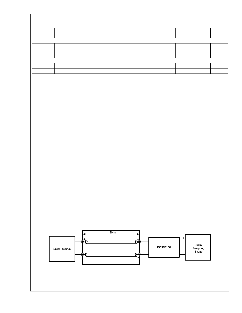
Test Setup Diagram
TEST CHANNEL USED IN PRODUCTION TEST, TYPICAL EYE DIAGRAMS
The test channel used in production test and typical eye diagram is a FR4 stripline test channel that can be practically
implemented in production load board environment, and yet with loss characteristics similar to a backplane that intended to
test the device's equalization span.
20096816
EQ50F100
www.national.com
4

Functional Description
The EQ50F100 6.25Gbps Backplane Equalizer is a fixed,
receive-end backplane equalizer. It enables serial transmis-
sion over FR-4 backplane with trace length of at least 30" at
6.25Gbps. It consists of an equalizer filter, limiting amplifier,
offset driver, and offset cancellation circuit. The equalizer
block compensates for the high frequency attenuation
caused by the bandwidth-limited transmission channel found
in backplane system. The limiting amplifier boost the signal
at the output of the equalizer block. The offset cancellation
circuit corrects for internal mis-match and offset from the
previous stage to minimize duty-cycle distortion.
Input and Output
The input and output stage of the EQ50F100 is implemented
using current mode logic (CML). The input stage has an
equivalent DC differential input resistance of 100
. The
positive and negative output channels are internally termi-
nated with a 50
pull-up to VDD. AC coupling is recom-
mended for both input and output.
Application Information
PCB LAYOUT AND POWER SYSTEM
CONSIDERATIONS
Power system performance may be greatly improved by
using thin dielectrics (2 to 4 mils) for power / ground sand-
wiches. This arrangement provides plane capacitance for
the PCB power system with low-inductance parasitic. Exter-
nal bypass capacitors should include both RF ceramic and
tantalum electrolytic types. RF capacitors may use values in
the range of 0.1nF to 10nF. Tantalum capacitors may be in
the 2.2uF to 10uF range. Voltage rating of the tantalum
capacitors should be at least 5X the power supply voltage
being used.
It is a recommended practice to use two vias at each power
pin as well as at all RF bypass capacitor terminals. Dual vias
reduce the interconnect inductance by up to half, thereby
reducing interconnect inductance and extending the effec-
tive frequency range of the bypass components. Locate RF
capacitors as close as possible to the supply pins, and use
wide low impedance traces (not 50 Ohm traces). Surface
mount capacitors are recommended due to their smaller
parasitics. It is recommended to connect power and ground
pins directly to the power and ground planes with bypass
capacitors connected to the plane with via on both ends of
the capacitor. Connecting power or ground pins to an exter-
nal bypass capacitor will increase the inductance of the path.
A small body size X7R chip capacitor, such as 0603 or 0402,
is recommended for external bypass. Its small body size
reduces the parasitic inductance of the capacitor. The user
must pay attention to the resonance frequency of these
external bypass capacitors, usually in the range of 20-30
MHz range. To provide effective bypassing, multiple capaci-
tors are often used to achieve low impedance between the
supply rails over the frequency of interest. At high frequency,
it is also a common practice to use two vias from power and
ground pins to the planes, reducing the impedance at high
frequency.
See AN-1187 for additional information on LLP package.
AC COUPLING
For multi-giga bit design, the smallest available package
should be used for the AC coupling capacitor. This will help
minimize degradation of signal quality due to package para-
sitics. The most common used capacitor value for the
EQ50F100 interface is 0.1uF capacitor.
EQ50F100
www.national.com
5