LM2747
Synchronous Buck Controller with Pre-bias Startup, and
Optional Clock Synchronization
General Description
The LM2747 is a high-speed synchronous buck regulator
controller with a feedback voltage accuracy of
�
1%. It can
provide simple down conversion to output voltages as low as
0.6V. Though the control section of the IC is rated for 3 to 6V,
the driver section is designed to accept input supply rails as
high as 14V. The use of adaptive non-overlapping MOSFET
gate drivers helps avoid potential shoot-through problems
while maintaining high efficiency. The IC is designed for the
more cost-effective option of driving only N-channel MOS-
FETs in both the high-side and low-side positions. It senses
the low-side switch voltage drop for providing a simple,
adjustable current limit.
The LM2747 features a fixed-frequency voltage-mode PWM
control architecture which is adjustable from 50 kHz to 1
MHz with one external resistor. In addition, the LM2747 also
allows the switching frequency to be synchronized to an
external clock signal over the range of 250 kHz to 1 MHz.
This wide range of switching frequency gives the power
supply designer the flexibility to make better tradeoffs be-
tween component size, cost and efficiency.
Features include the ability to startup with a pre-biased load
on the output, soft-start, input undervoltage lockout (UVLO)
and Power Good (based on both undervoltage and overvolt-
age detection). In addition, the shutdown pin of the IC can be
used for providing startup delay, and the soft-start pin can be
used for implementing precise tracking, for the purpose of
sequencing with respect to an external rail.
Features
n
�
1% feedback voltage accuracy over temperature
n
Switching frequency from 50 kHz to 1 MHz
n
Switching frequency synchronize range 250 kHz to 1
MHz
n
Startup with a pre-biased output load
n
Power stage input voltage from 1V to 14V
n
Control stage input voltage from 3V to 6V
n
Output voltage adjustable down to 0.6V
n
Power Good flag and shutdown
n
Output overvoltage and undervoltage detection
n
Low-side adjustable current sensing
n
Adjustable soft-start
n
Tracking and sequencing with shutdown and soft start
pins
n
TSSOP-14 package
Applications
n
Down Conversion from 3.3V
n
Cable Modem, DSL and ADSL
n
Laser Jet and Ink Jet Printers
n
Low Voltage Power Modules
n
DSP, ASIC, Core and I/O
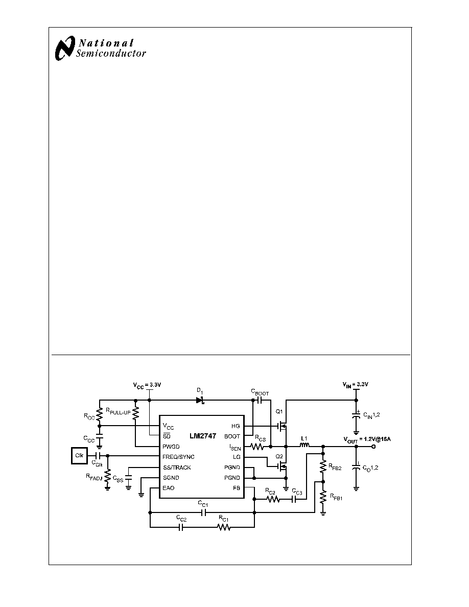
Typical Application
20150901
March 2006
LM2747
Synchronous
Buck
Controller
with
Pre-bias
Startup,
and
Optional
Clock
Synchronization
� 2006 National Semiconductor Corporation
DS201509
www.national.com
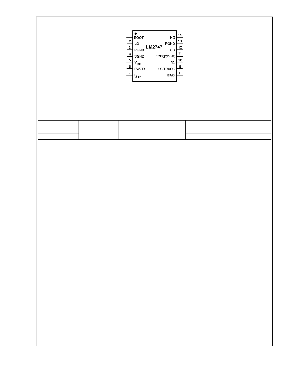
Connection Diagram
20150990
14-Lead Plastic TSSOP
JA
= 155�C/W
NS Package Number MTC14
Ordering Information
Order Number
Package Type
NSC Package Drawing
Supplied As
LM2747MTC
TSSOP-14
MTC14
94 Units on Rail
LM2747MTCX
2500 Units on Tape and Reel
Pin Description
BOOT (Pin 1) - Bootstrap pin. This is the supply rail for the
high-side gate driver. When the high-side MOSFET turns on,
the voltage on this pin should be at least one gate threshold
above the regulator input voltage V
IN
to properly turn on the
MOSFET. See MOSFET Gate Drivers in the Application
Information section for more details on how to select MOS-
FETs.
LG (Pin 2) - Low-gate drive pin. This is the gate drive for the
low-side N-channel MOSFET. This signal is interlocked with
the high-side gate drive HG (Pin 14), so as to avoid shoot-
through.
PGND (Pins 3, 13) - Power ground. This is also the ground
for the low-side MOSFET driver. Both the pins must be
connected together on the PCB and form a ground plane,
which is usually also the system ground.
SGND (Pin 4) - Signal ground. It should be connected
appropriately to the ground plane with due regard to good
layout practices in switching power regulator circuits.
V
CC
(Pin 5) Supply rail for the control sections of the IC.
PWGD (Pin 6) - Power Good pin. This is an open drain
output, which is typically meant to be connected to V
CC
or
any other low voltage source through a pull-up resistor.
Choose the pull-up resistor so that the current going into this
pin is kept below 1 mA. A recommended value for the pull-up
resistor is 100 k
for most applications. The voltage on this
pin is thus pulled low under output undervoltage or overvolt-
age fault conditions and also under input UVLO.
I
SEN
(Pin 7) - Current limit threshold setting pin. This sources
a fixed 40 �A current. A resistor of appropriate value should
be connected between this pin and the drain of the low-side
MOSFET (switch node). The minimum value for this resistor
is 1 k
.
EAO (Pin 8) - Output of the error amplifier. The voltage level
on this pin is compared with an internally generated ramp
signal to determine the duty cycle. This pin is necessary for
compensating the control loop.
SS/TRACK (Pin 9) - Soft-start and tracking pin. This pin is
internally connected to the non-inverting input of the error
amplifier during soft-start, and in fact any time the SS/
TRACK pin voltage happens to be below the internal refer-
ence voltage. For the basic soft-start function, a capacitor of
minimum value 1 nF is connected from this pin to ground. To
track the rising ramp of another power supply's output, con-
nect a resistor divider from the output of that supply to this
pin as described in Application Information.
FB (Pin 10) - Feedback pin. This is the inverting input of the
error amplifier, which is used for sensing the output voltage
and compensating the control loop.
FREQ/SYNC (Pin 11) - Frequency adjust pin. The switching
frequency is set by connecting a resistor of suitable value
between this pin and ground. Some typical values (rounded
up to the nearest standard values) are 150 k
for 200 kHz,
100 k
for 300 kHz, 51.1 k for 500 kHz, 18.7 k for 1 MHz.
This pin is also used to synchronize to an external clock
within the range of 250kHz to 1MHz.
SD (Pin 12) - IC shutdown pin. Pull this pin to V
CC
to ensure
the IC is enabled. Connect to ground to disable the IC. Under
shutdown, both high-side and low-side drives are off. This
pin also features a precision threshold for power supply
sequencing purposes, as well as a low threshold to ensure
minimal quiescent current.
HG (Pin 14) - High-gate drive pin. This is the gate drive for
the high-side N-channel MOSFET. This signal is interlocked
with LG (Pin 2) to avoid shoot-through.
LM2747
www.national.com
2

Absolute Maximum Ratings
(Note 1)
If Military/Aerospace specified devices are required,
please contact the National Semiconductor Sales Office/
Distributors for availability and specifications.
V
CC
-0.3 to 7V
BOOT Voltage
-0.3 to 18V
I
SEN
-0.3 to 14V
FREQ/SYNC Voltage
-0.5 to V
CC
+ 0.3V
All other pins
-0.3 to V
CC
+ 0.3V
Junction Temperature
150�C
Storage Temperature
-65�C to 150�C
Soldering Information
Lead Temperature (soldering, 10sec)
260�C
Infrared or Convection (20sec)
235�C
ESD Rating (Note 3)
2kV
Operating Ratings
Supply Voltage Range, V
CC
(Note 2)
3V to 6V
BOOT Voltage Range
1V to 17V
Junction Temperature Range (T
J
)
-40�C to +125�C
Thermal Resistance (
JA
)
155�C/W
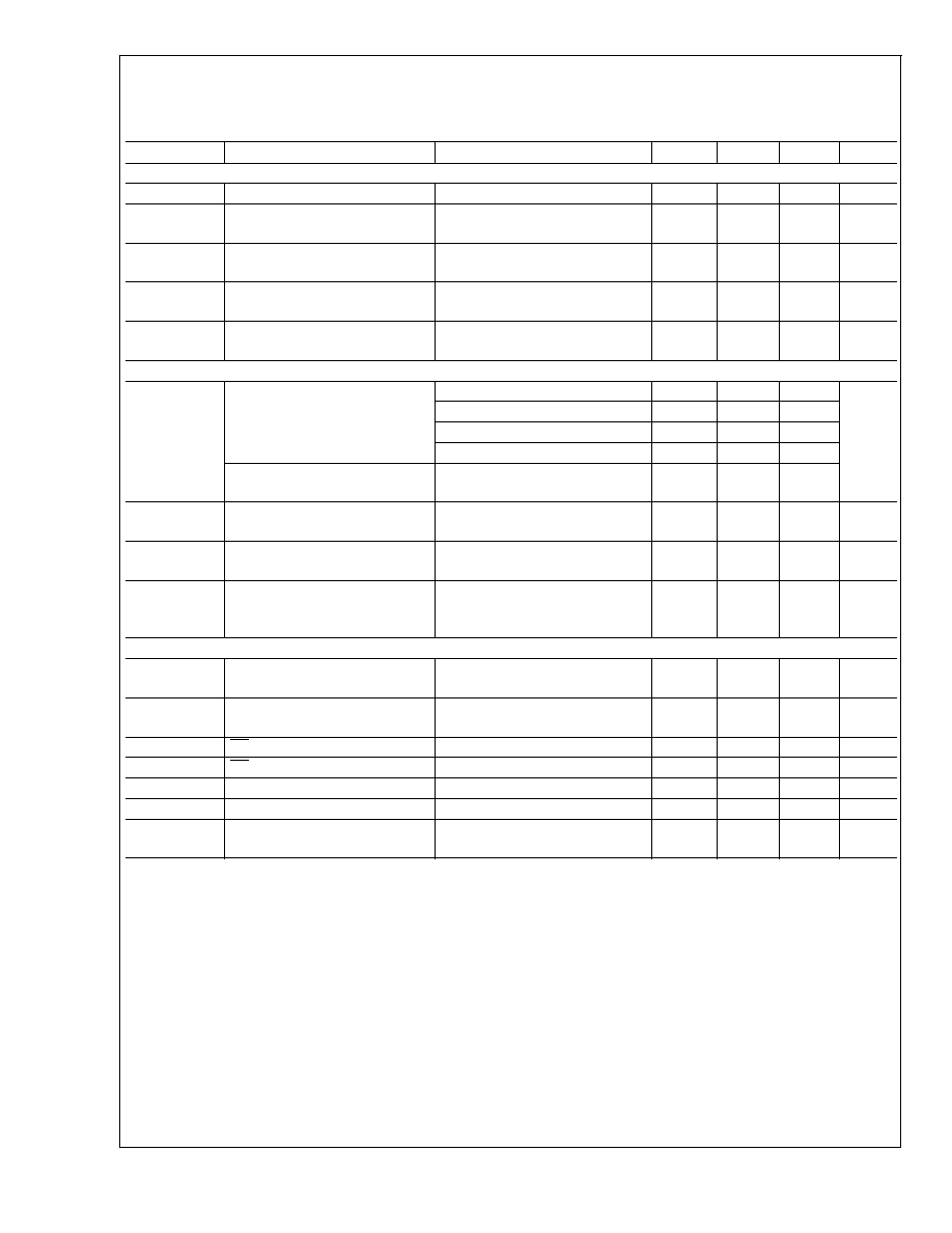
Electrical Characteristics
V
CC
= 3.3V unless otherwise indicated. Typicals and limits appearing in plain type apply for T
A
= T
J
= 25�C. Limits appearing in
boldface type apply over full Operating Temperature Range. Datasheet min/max specification limits are guaranteed by design,
test, or statistical analysis.
Symbol
Parameter
Conditions
Min
Typ
Max
Units
V
FB
FB Pin Voltage
V
CC
= 3V to 6V
0.594
0.6
0.606
V
V
ON
UVLO Thresholds
V
CC
Rising
V
CC
Falling
2.79
2.42
V
I
Q_VCC
Operating V
CC
Current
V
CC
= 3.3V, V
SD
= 3.3V
f
SW
= 600 kHz
1.1
1.7
2.3
mA
V
CC
= 5V, V
SD
= 3.3V
f
SW
= 600 kHz
1.3
2
2.6
Shutdown V
CC
Current
V
CC
= 3.3V, V
SD
= 0V
1
3
�A
t
PWGD1
PWGD Pin Response Time
V
FB
Rising
10
�s
t
PWGD2
PWGD Pin Response Time
V
FB
Falling
10
�s
I
SS-ON
SS Pin Source Current
V
SS
= 0V
7
10
14
�A
I
SS-OC
SS Pin Sink Current During Over
Current
V
SS
= 2.0V
90
�A
I
SEN-TH
I
SEN
Pin Source Current Trip
Point
25
40
55
�A
I
FB
FB Pin Current
Sourcing
20
nA
ERROR AMPLIFIER
GBW
Error Amplifier Unity Gain
Bandwidth
9
MHz
G
Error Amplifier DC Gain
118
dB
SR
Error Amplifier Slew Rate
2
V/�s
I
EAO
EAO Pin Current Sourcing and
Sinking Capability
14
16
mA
V
EAO
Error Amplifier Output Voltage
Minimum
1
V
Maximum
2.2
V
LM2747
www.national.com
3
Electrical Characteristics
(Continued)
V
CC
= 3.3V unless otherwise indicated. Typicals and limits appearing in plain type apply for T
A
= T
J
= 25�C. Limits appearing in
boldface type apply over full Operating Temperature Range. Datasheet min/max specification limits are guaranteed by design,
test, or statistical analysis.
Symbol
Parameter
Conditions
Min
Typ
Max
Units
GATE DRIVE
I
Q-BOOT
BOOT Pin Quiescent Current
V
BOOT
= 12V, V
SD
= 0
18
90
�A
R
HG_UP
High-Side MOSFET Driver
Pull-Up ON resistance
V
BOOT
= 5V
@
350 mA Sourcing
2.7
R
HG_DN
High-Side MOSFET Driver
Pull-Down ON resistance
350 mA Sinking
0.8
R
LG_UP
Low-Side MOSFET Driver Pull-Up
ON resistance
V
BOOT
= 5V
@
350 mA Sourcing
2.7
R
LG_DN
Low-Side MOSFET Driver
Pull-Down ON resistance
350 mA Sinking
0.8
OSCILLATOR
f
SW
PWM Frequency
R
FADJ
= 750 k
50
kHz
R
FADJ
= 100 k
300
R
FADJ
= 42.2 k
475
600
725
R
FADJ
= 18.7 k
1000
External Synchronizing Signal
Frequency
Voltage Swing = 0V to V
CC
250
1000
SYNC
L
Synchronization Signal Low
Threshold
f
SW
= 250 kHz to 1 MHz
1
V
SYNC
H
Synchronization Signal High
Threshold
f
SW
= 250 kHz to 1 MHz
2
V
D
MAX
Max High-Side Duty Cycle
f
SW
= 300 kHz
f
SW
= 600 kHz
f
SW
= 1 MHz
86
78
67
%
LOGIC INPUTS AND OUTPUTS
V
STBY-IH
Standby High Trip Point
V
FB
= 0.575V, V
BOOT
= 3.3V
V
SD
Rising
1.1
V
V
STBY-IL
Standby Low Trip Point
V
FB
= 0.575V, V
BOOT
= 3.3V
V
SD
Falling
0.232
V
V
SD-IH
SD Pin Logic High Trip Point
V
SD
Rising
1.3
V
V
SD-IL
SD Pin Logic Low Trip Point
V
SD
Falling
0.8
V
V
PWGD-TH-LO
PWGD Pin Trip Points
V
FB
Falling
0.408
0.434
0.457
V
V
PWGD-TH-HI
PWGD Pin Trip Points
V
FB
Rising
0.677
0.710
0.742
V
V
PWGD-HYS
PWGD Hysteresis
V
FB
Falling
V
FB
Rising
60
90
mV
Note 1: Absolute maximum ratings indicate limits beyond which damage to the device may occur. Operating ratings indicate conditions for which the device
operates correctly. Operating Ratings do not imply guaranteed performance limits.
Note 2: The power MOSFETs can run on a separate 1V to 14V rail (Input voltage, V
IN
). Practical lower limit of V
IN
depends on selection of the external MOSFET.
See the MOSFET GATE DRIVERS section under Application Information for further details.
Note 3: ESD using the human body model which is a 100pF capacitor discharged through a 1.5 k
resistor into each pin.
LM2747
www.national.com
4
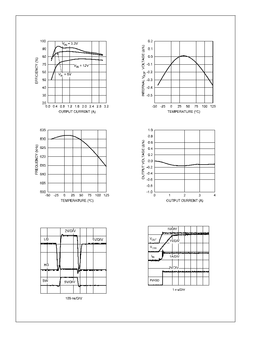
Typical Performance Characteristics
Efficiency (V
OUT
= 1.2V)
V
CC
= 3.3V, f
SW
= 1 MHz
Internal Reference Voltage vs Temperature
20150940
20150958
Frequency vs Temperature
Output Voltage vs Output Current
20150960
20150956
Switch Waveforms
V
CC
= 3.3V, V
IN
= 5V, V
OUT
= 1.2V
I
OUT
= 3A, C
SS
= 12 nF, f
SW
= 1 MHz
Start-Up (Full-Load)
V
CC
= 3.3V, V
IN
= 5V, V
OUT
= 1.2V
I
OUT
= 3A, C
SS
= 12 nF, f
SW
= 1 MHz
20150946
20150948
LM2747
www.national.com
5