 | –≠–ª–µ–∫—Ç—Ä–æ–Ω–Ω—ã–π –∫–æ–º–ø–æ–Ω–µ–Ω—Ç: FPD33584 | –°–∫–∞—á–∞—Ç—å:  PDF PDF  ZIP ZIP |
FPD33584
Low Power, Low EMI, TFT-LCD Column Driver with
RSDS Inputs, 64 Grayshades, and 384 Outputs for
XGA/SXGA Applications
General Description
The FPD33584 Column Driver is a direct drive, 64 gray level,
384 output, TFT-LCD column driver with an RSDS
TM
data
interface. It provides the capability to display 262,144 colors
(18-bit color) with a large dynamic output range for twisted
nematic applications. When used in a bank with other
FPD33584 column drivers, the FPD33584 can support XGA
(8 drivers) or SXGA (10 drivers) applications. Output volt-
ages are gamma corrected to provide a direct mapping
between digital video and LCD panel brightness. The 85MHz
operating frequency allows the FPD33584 to meet the re-
quirement of high refresh rate applications (i.e. XGA moni-
tors with a 75Hz refresh rate).
An RSDS (Reduced Swing Differential Signaling) interface is
used between the timing controller and the column driver to
minimize EMI and reduce power.
Features
n
RSDS (Reduced Swing Differential Signaling) data bus
for low power, reduced EMI and small PCB foot print
n
85MHz maximum operating frequency at V
DD1
=3.0V
(70MHz at V
DD1
=2.7V)
n
Pin compatible with Samsung S6C0666
n
Ideal for XGA and SXGA applications
n
Supports notebook and monitor applications
n
Smart Charge Conservation for low power consumption
n
64 Gray levels per color (18-bit color)
n
Supports both Dot and N-Line inversion
n
Four externally programmable gamma curves
n
Low offset, High voltage outputs for high contrast in a
large range of display panel applications
n
Optional, high current, repair amplifiers
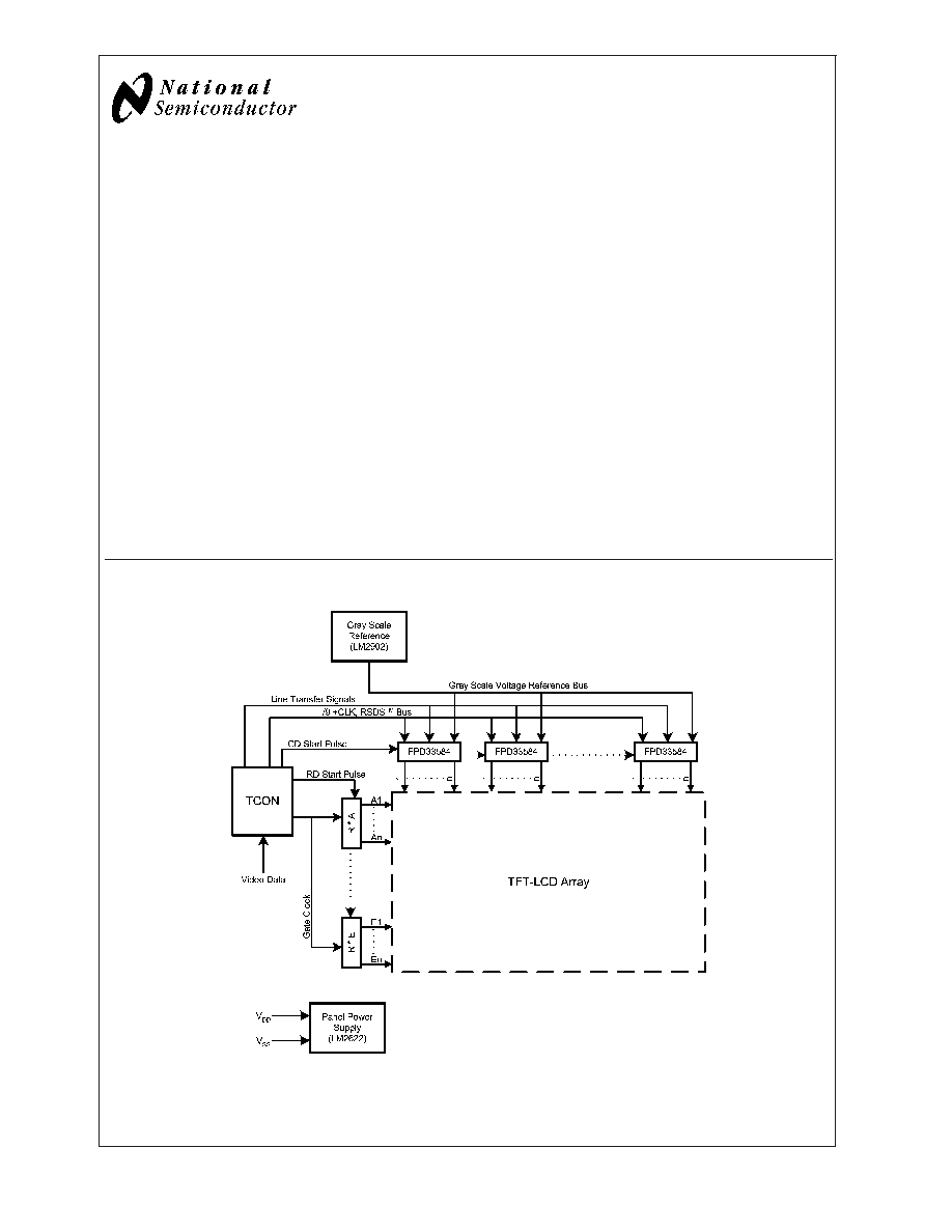
System Diagram
20043201
January 2003
FPD33584
Low
Power
,
Low
EMI,
TFT
-LCD
Column
Driver
with
RSDS
Inputs,
64
Grayshades,
and
384
Outputs
for
XGA/SXGA
Applications
© 2003 National Semiconductor Corporation
DS200432
www.national.com
Absolute Maximum Ratings
(Note 1)
Analog Supply, (V
DD2
) (Note 2)
-0.3V to +11.5V
Logic Supply, (V
DD1
) (Note 2)
-0.3V to +5.0V
Low-Polarity RDAC Reference
Voltages, (V
GMA6
to V
GMA10
)
(Note 2)
-0.3V to 0.5V
DD2
High-Polarity RDAC Reference
Voltages, (V
GMA1
to V
GMA5
)
(Note 2)
0.5V
DD2
- 1.0V to
V
DD2
+ 0.3V
RDAC Current (All Gamma
Voltage
Taps), (I
GMA
to I
GMA10
)
-2.5mA to 2.5mA
Input Voltage (Digital Logic), (V
IN
)
(Note 2)
-0.3V to V
DD1
+
0.3V
Output Voltage, (V
OUT
) (Note 2)
-0.3V to V
DD2
+
0.3V
Output Current (Analog), (I
OUT
)
-7mA to +7mA
Storage Temperature Range, (T
S
)
-55∞C to +125∞C
Note 1: "Absolute Maximum Ratings" are those values beyond which the
safety of the device cannot be guaranteed. They are not meant to imply that
the devices should be operated at these limits. The table of "Electrical
Characteristics" specifies conditions of device operation.
Note 2: Absolute voltages referenced to V
SS1
= V
SS2
= 0.0V.
Recommended Operating
Conditions
Min
Typ
Max
Units
Logic Supply Voltage
(V
DD1
)
2.7
3.3
3.6
V
Supply Voltage (V
DD2
)
7.5
10.5
V
Operating Temperature
(T
A
)
-10
+25
+70
∞C
DC Electrical Characteristics
Digital Electrical Characteristics
Symbol
Parameter
Conditions
Min
Typ
Max
Units
V
IH
Logic Input High Voltage
0.7 V
DD1
V
V
IL
Logic Input Low Voltage
0.3 V
DD1
V
V
OH
Logic Output High Voltage
I
OH
= -0.5mA
V
DD1
-
0.5
V
V
OL
Logic Output Low Voltage
I
OL
= 0.5mA
0.5
V
I
DD1
Logic Current
(Note 3)
8.0
12.0
mA
I
IH
Input Leakage
V
DD1
= 3.6V, V
IN
= 3.6V
-1
1
µA
I
IL
Input Leakage
V
DD1
= 3.6V, V
IN
= 0V
-1
1
µA
C
IN
Input Capacitance
All logic pins
2
pF
Note 3: CLK frequency = 67MHz, V
DD1
= 3.3V, V
SS1
= V
SS2
= 0.0V, line time = 18µs, data = all 1's for 4 lines followed by all 0's for 4 lines.
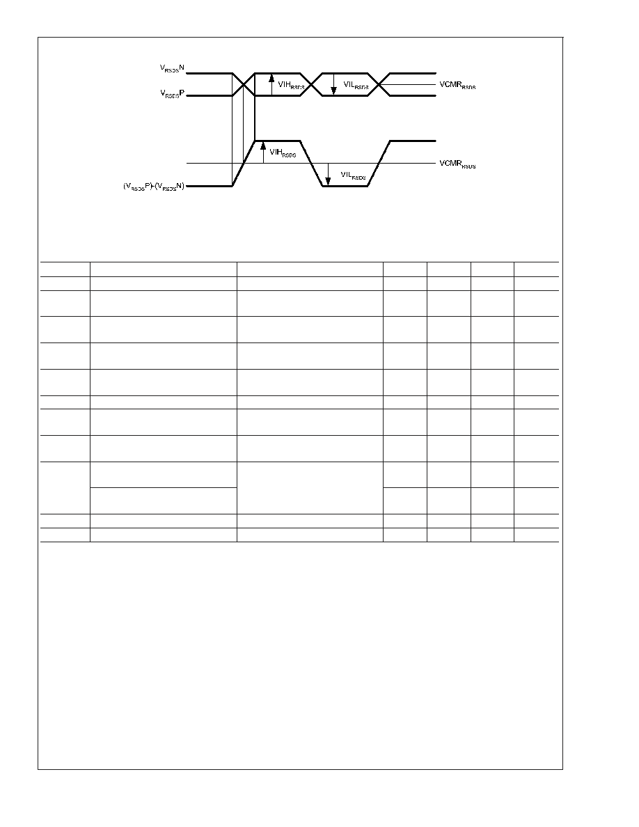
RSDS Characteristics
Symbol
Parameter
Conditions
Min
Typ
Max
Units
VIH
RSDS
RSDS High Input Voltage
VCM
RSDS
= 1.2V (Note 4) see
Figure 1
100
200
mV
VIL
RSDS
RSDS Low Input Voltage
VCM
RSDS
= 1.2V (Note 4) see
Figure 1
-200
-100
mV
VCM
RSDS
RSDS Common Mode Input
Voltage Range
VIH
RSDS
= +100mV, VIL
RSDS
=
-100mV (Note 5) see Figure 1
V
SS1
+
0.1
V
DD1
-
1.3
V
IDL
RSDS Input Leakage Current
DxxP, DxxN, CLKP, CLKN
-10
10
µA
Note 4: VCM
RSDS
= (VCLKP + VCLKN)/2 or (VDxxP + VDxxN)/2.
Note 5: VIH
RSDS
and VIL
RSDS
are referenced to VCMR
RSDS
FPD33584
www.national.com
2
Analog Electrical Characteristics
Symbol
Parameter
Conditions
Min
Typ
Max
Units
I
DD2
Supply Current Consumption
(Note 6)
5.0
12.0
mA
V
GMA1
Upper RDAC High Side Input
(Note 7)
V
DD2
/2 +
0.2
V
DD2
-
0.2
V
V
GMA5
Upper RDAC Low Side Input
(Note 7)
V
DD2
/2 +
0.2
V
DD2
-
0.2
V
V
GMA6
Lower RDAC High Side Input
(Note 7)
0.2
V
DD2
/2 -
0.2
V
V
GMA10
Lower RDAC Low Side Input
(Note 7)
0.2
V
DD2
/2 -
0.2
V
C
LOAD
Output Capacitive Load
30
150
pF
V
OUT
Output Voltage Range
V
SS2
+
0.2
V
DD2
-
0.2
V
R
DAC
RDAC References (V
GMA1
to
V
GMA5
and V
GMA6
to V
GMA10
)
each
12.0
15.0
18.0
k
V
pperr
Output Peak to Peak Error (gray
levels 0 through 58)
V
GMA1
= V
DD2
- TBDV
V
GMA10
= V
SS2
+ TBDV
(Note 8)
±
3
±
12
mV
Output Peak to Peak Error (gray
levels 59 through 63)
±
5
±
25
mV
V
parterr
Output Part to Part Error
(Note 9)
±
5
mV
I
OUT RP
Repair Buffer Output Current
(Note 10)
±
2
±
3
mA
Note 6: V
DD2
= 10V, V
DD1
= 3.3V, f
CLK
= 67MHz, line time = 18µsec, data = maximum output swing (GMA1 to GMA10), [TIME1, TIME0] = [0,1] (charge sharing of
32 clock cycles
Note 7: The following relationship must be maintained between the reference voltages: V
DD2
>
V
GMA1
>
V
GMA2
>
V
GMA3
>
V
GMA4
>
V
GMA5
>
V
GMA6
>
V
GMA7
>
V
GMA8
>
V
GMA9
>
V
GMA10
>
V
SS2
Note 8: V
pperr
is meant to reflect the error in peak-to-peak output voltage for each gray level whent the output swings from the high value VHxx to the low value
VLxx. This parameter applies to every output on the die. The typical value represents one standard deviation from ideal based on tester data. The maximum value
is a constraint of the test environment, not the performance of the part.
Note 9: V
parterr
is meant to guarantee the part-to-part output variation. The average of all outputs at gray level 32 is compared to a nominal gray level 32 value. The
difference is V
parterr
Note 10: Current into device pins is defined as positive. Current out of device pins is defined as negative. |V
OUT
- V
IN
|
>
500mV.
20043202
FIGURE 1. RSDS Signal Definition
FPD33584
www.national.com
3
AC Electrical Characteristics
Digital AC Characteristics
Symbol
Parameter
Conditions
Min
Typ
Max
Units
PW
CLK
Clock Period
V
DD1
= 2.7 to 3.0V
14
ns
PW
CLK
Clock Period
V
DD1
= 3.0 to 3.6V
11.7
ns
PW
CLK(L)
Low Clock Pulse Width
40%
60%
PW
CLK
PW
CLK(H)
High Clock Pulse Width
40%
60%
PW
CLK
t
setup1
RSDS Data Setup Time
2
ns
t
hold1
RSDS Data Hold Time
0
ns
t
setup2
ENIOx Setup Time
2
ns
t
hold2
ENIOx Hold Time
4
ns
t
PLH1
Start Pulse Fall Delay
C
LINE
= 15 pF
8
ns
PW
DIO
ENIOx Pulse Width
1
2
PW
CLK
PW
CLK1
LOAD Pulse Width
5 T
CLK
5µs
t
LDT
Last Clock to LOAD Delay
1
PW
CLK
t
DENSU
LOAD to First ENIO Setup
2
PW
CLK
tPOL≠CLK1
POL≠CLK1 Time
14
ns
Analog AC Characteristics
Supplies: V
SS1
= V
SS2
= 0.0V, V
DD1
= 3.3V, V
DD2
= +10.0V.
Symbol
Parameter
Conditions
Min
Typ
Max
Units
t
settle 90%
Output Settling Time to 90% of
Final Value
Figure 2 (Note 11)
6
µs
t
6-bit accy
Output Settling Time to 6-bit
accuracy
(Note 11)
10
µs
t
RP 90%
Repair Line Output Settling Time to
90% of Final Value
C
LOAD
= 150 pF,
(Note 11)
6
µs
t
RP 6-bit accy
Repair Line Output Settling Time to
6-bit accuracy
C
LOAD
= 150 pF,
(Note 11)
10
µs
Note 11: V
GMA1
= 9.8V, V
GMA10
= 0.2V, V
GMA5
= 5.2V, V
GMA6
= 4.8V, [TIME0, TIME1] = [0,1].
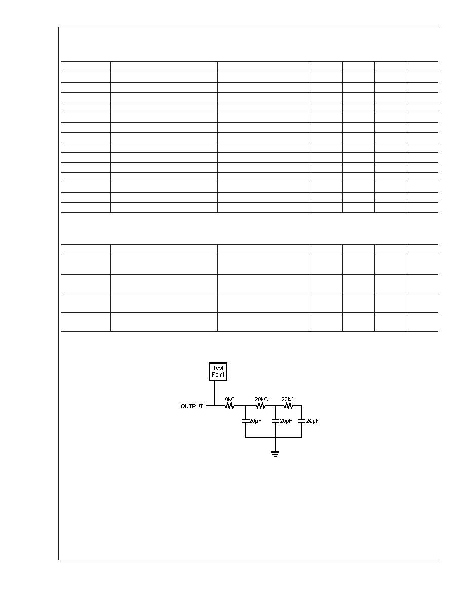
20043211
FIGURE 2. Test Circuit for Output Settling Time Measurements
FPD33584
www.national.com
4
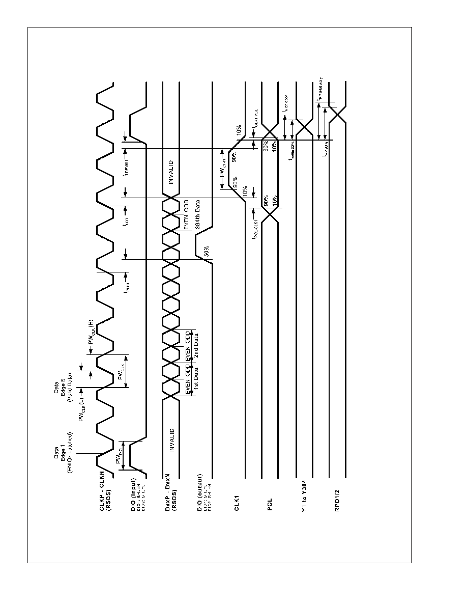
Timing
Diagrams
20043203
FPD33584
www.national.com
5