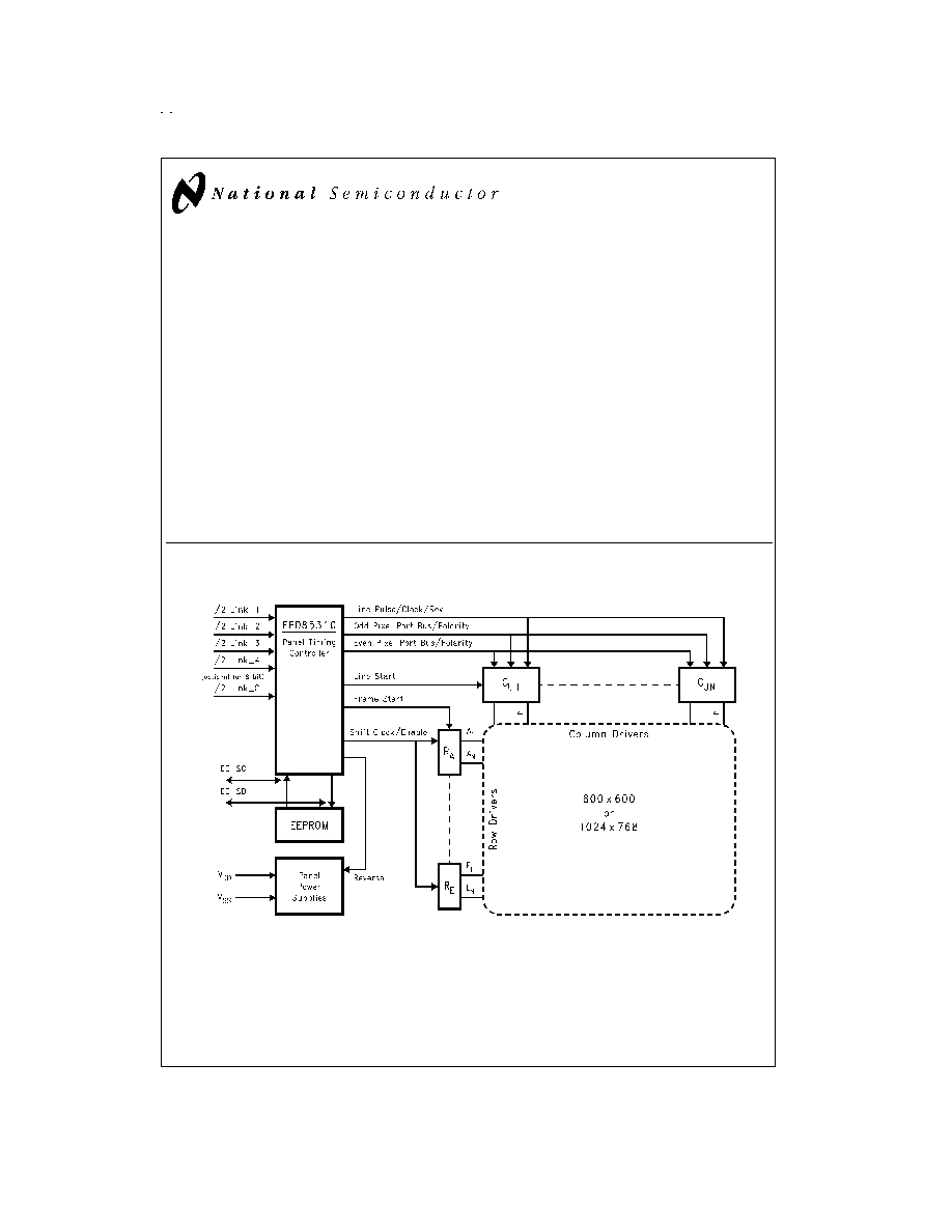
FPD85310
Panel Timing Controller
General Description
The FPD85310 Panel Timing Controller is an integrated
FPD-Link based TFT-LCD timing controller. It resides on the
flat panel display and provides the interface signal routing
and timing control between graphics or video controllers and
a TFT-LCD system. FPD-Link is a low power, low electro-
magnetic interference interface used between this controller
and the host system.
The FPD85310 chip links the panel's system interface to the
display via a ten wire LVDS data bus. That data is then
routed to the source and gate display drivers. XGA and
SVGA resolutions are supported.
The FPD85310 is programmable via an optional external se-
rial EEPROM. Reserved space in the EEPROM is available
for display identification information. The system can access
the EEPROM to read the display identification data or pro-
gram initialization values used by the FPD85310.
Features
n
FPD-Link System Interface utilizes Low Voltage
Differential Signaling (LVDS).
n
System programmable via EEPROM
n
Suitable for notebook and monitor applications
n
8-bit or 6-bit system interface
n
XGA or SVGA capable
n
Supports single or dual port column drivers
n
Programmable outputs provide customized control for
standard or in-house column drivers and row drivers
n
Fail-safe operation prevents panel damage with system
clock failure
n
Programmable skew rate controlled outputs on CD
interface for reduced EMI
n
Polarity pin reduces CD data bus switching
n
CMOS circuitry operates from a 3.3V supply
System Diagram
TRI-STATE
Æ
is a registered trademark of National Semiconductor Corporation.
DS101086-1
September 1999
FPD85310
Panel
T
iming
Controller
© 1999 National Semiconductor Corporation
DS101086
www.national.com
Absolute Maximum Ratings
(Note 1)
If Military/Aerospace specified devices are required,
please contact the National Semiconductor Sales Office/
Distributors for availability and specifications.
Supply Voltage (V
DD
)
4.1V
DC Input Voltage (V
IN
)
-0.5V to V
DD
+0.5V
DC Output Voltage (V
OUT
)
-0.5V to V
DD
+0.5V
Storage Temperature Range
(T
STG
)
-65∞C to +150∞C
Lead Temperature (T
L
)
(Soldering 10 sec.)
260∞C
ESD Rating:
(C
ZAP
= 120 pF, R
ZAP
= 1500
)
MM = 200V, HBM = 2000V
Operating Conditions
Min
Max
Units
Supply Voltage (V
DD
)
3.0
3.6
V
Operating Temp. Range (T
A
)
0
70
∞C
Note 1: "Absolute Maximum Ratings" are those values beyond which the
safety of the device cannot be guaranteed. They are not meant to imply that
the devices should be operated at these limits. The table of "Electrical Char-
acteristics" specifies conditions of device operation.
DC Electrical Characteristics
T
A
= 0∞C to 70∞C, V
DD
= 3.3V
±
0.3V (unless otherwise specified)
Symbol
Parameter
Conditions
Min
Max
Units
V
OH
Minimum High Level
Output Voltage
V
DD
= 3.0V, I
OH
= 1 mA
2.4
V
V
OL
Maximum Low Level
Output Voltage
V
DD
= 3.0V, I
OL
= 1 mA
0.4
V
V
IH
Minimum High Level
Input Voltage
2.0
V
V
IL
Maximum Low Level
Input Voltage
0.8
V
I
IN
Input Current
V
IN
= V
DD
10
µA
I
OZ
Maximum TRI-STATE
Output Leakage Current
V
IN
= V
DD
, V
IN
= V
SS
10
µA
I
DD
Average Supply Current
f = 65 MHz, C
LOAD
= 50 pF
312
mA
V
THH
Differential Input High
Threshold
Common Mode Voltage = +1.2V
+100
mV
V
THL
Differential Input Low
Threshold
Common Mode Voltage = +1.2V
-100
mV
Device Specifications
T
A
= 0∞C to 70∞C, V
DD
= 3.3V (unless otherwise specified)
Symbol
Parameter
Conditions
Min
Max
Units
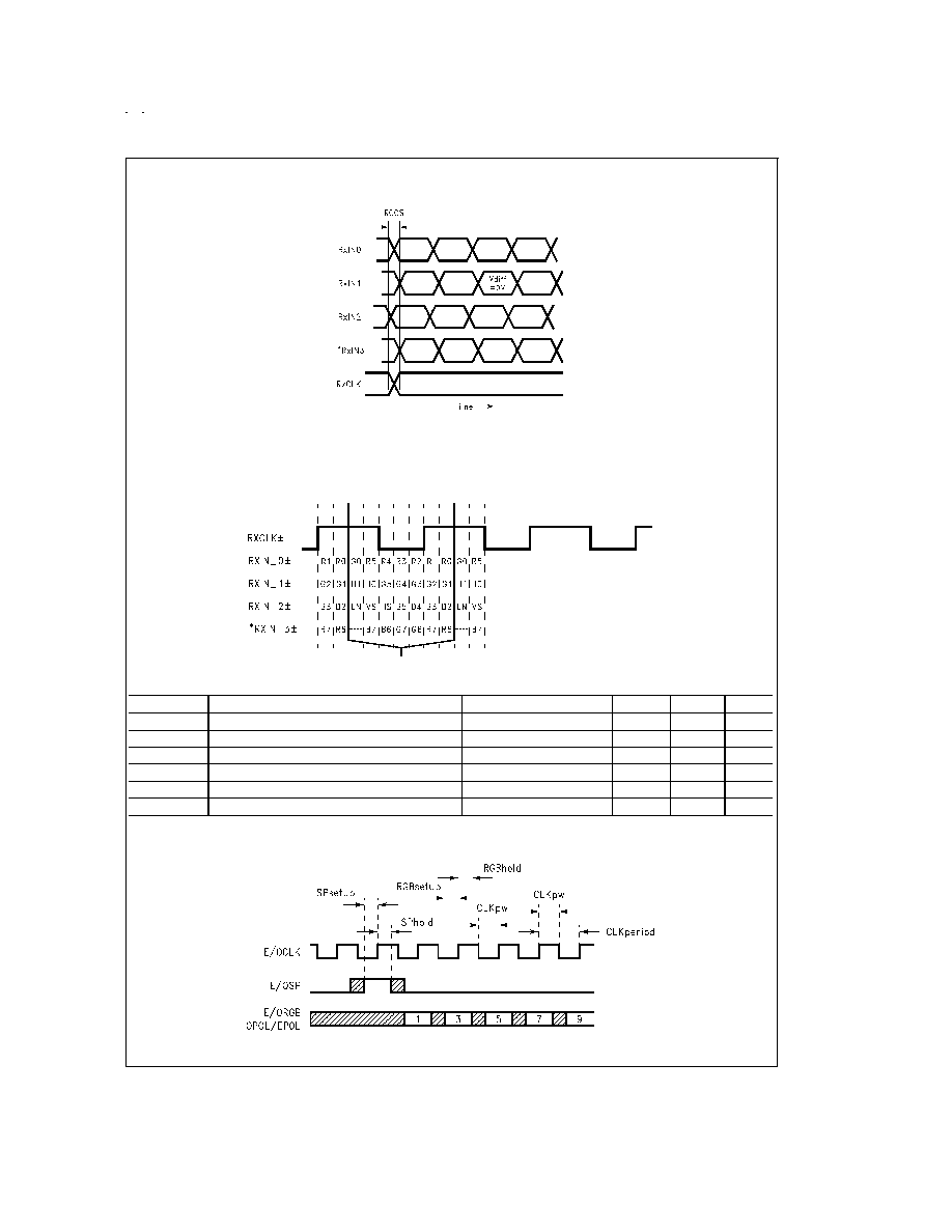
RPLLS
Receiver Phase Lock Loop Set Time
10
ms
RCCS
RxIN Channel-to-Channel Skew (Note 2)
700
ps
Note 2: This limit assumes a maximum cable skew of 350 ps. Actual automated test equipment limit is 400 ps due to tester accuracy.
DS101086-12
FIGURE 1. FPD85310 (Receiver) Phase Lock Loop Set Time
www.national.com
2
Device Specifications
T
A
= 0∞C to 70∞C, V
DD
= 3.3V (unless otherwise specified) (Continued)
Symbol
Parameter
Conditions
Min
Max
Units
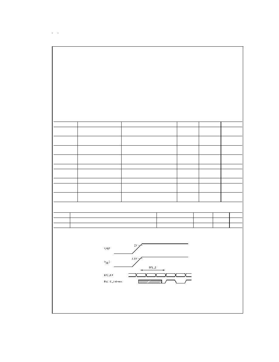
SPsetup
E/OSP from E/OCLK
65 MHz Video (Note 6)
8
ns
SPhold
E/OSP from E/OCLK
65 MHz Video (Note 6)
8
ns
RGBsetup
ER/EG/EB/OR/OG/OB from E/OCLK
65 MHz Video (Note 6)
8
ns
RGBhold
ER/EG/EB/OR/OG/OB from E/OCLK
65 MHz Video (Note 6)
8
ns
CLKpw
E/OCLK pulsewidth
65 MHz Video (Note 6)
11
ns
CLKperiod
E/OCLK period
65 MHz Video (Note 6)
25
ns
Note 6: Timing applies to Dual Bus output modes.
DS101086-13
Note 3: Measurements at V
DIFF
= 0V
Note 4: RCCS measured between earliest and latest LVDS edges
Note 5:
*
RxIN3 pair (RxIN_3
±
) is option for 24-bit color depth
FIGURE 2. FPD85310 (Receiver) Channel-to-Channel Skew and Pulse Width
DS101086-14
FIGURE 3. FPD85310's (Receiver) Format of the Input Data
DS101086-15
FIGURE 4. Column Driver Bus AC Timing
www.national.com
3
Device Specifications
T
A
= 0∞C to 70∞C, V
DD
= 3.3V (unless otherwise specified) (Continued)
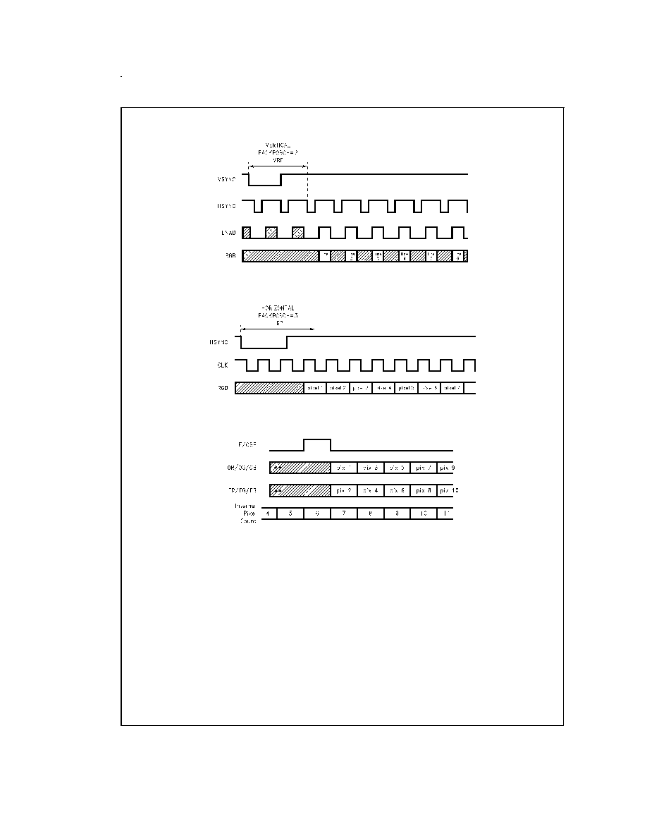
DS101086-16
FIGURE 5. Vertical Backporch Definition
(Video Data from Host)
DS101086-17
FIGURE 6. Horizontal Backporch Definition
(Video Data from Host)
DS101086-18
Internal Pixel Count final value = pixels per line/2
Maximum Internal Pixel Count = 1024 (32.5 MHz clocks)
Internal Pixel Count is used to generate the horizontal_component for GPO generation
See
Figure 9
**
Without Blanking control (GPO8), random data may be observed during 16 OCLK and discontinuous 1 OCLK before E/OSP, but it should not be affected to
actual image.
FIGURE 7. Internal Pixel Count Used for GPO Control Generation
www.national.com
4

Device Specifications
T
A
= 0∞C to 70∞C, V
DD
= 3.3V (unless otherwise specified) (Continued)
DS101086-19
LC = lines per frame count, LCmax = 2048 lines
Internal Line Count is used to generate the vertical component for GPO generation
See
Figure 9
FIGURE 8. Internal Line Count Used for GPO Control Generation
GPO Generation
DS101086-20
GPO Combination Select
DS101086-21
FIGURE 9. GPO Control Generation
www.national.com
5