FPD87208AXA
+2.5V Low EMI, Low Dynamic Power XGA/WXGA
TFT-LCD Timing Controller with Reduced Swing
Differential Signaling RSDS
TM
Outputs
General Description
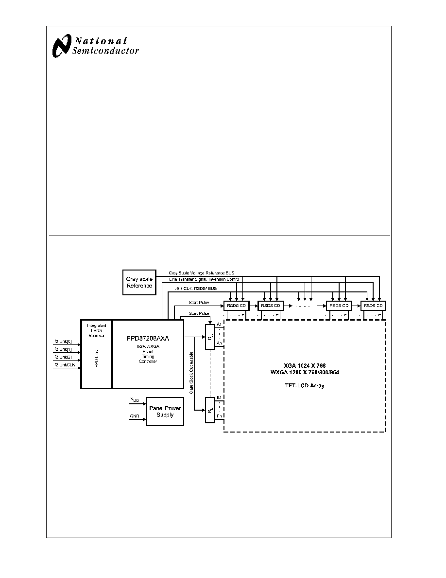
The FPD87208AXA is a timing controller that combines an
LVDS single pixel input interface with National Reduced
Swing Differential Signaling (RSDS
TM
) output driver interface
for XGA and Wide XGA resolutions. It resides on the TFT-
LCD panel and provides the data buffering and control signal
generation for XGA, and Wide XGA graphic modes. The
RSDS path to the column driver contributes toward lowering
radiated EMI and reducing system dynamic power consump-
tion.
This single RSDS bus conveys the 6-bit color data for XGA,
and three different WXGA resolutions.
Features
n
Reduced Swing Differential Signaling (RSDS) digital bus
reduces dynamic power, EMI and bus-width from the
timing controller
n
LVDS single pixel input interface system
n
Input clock range from 25 MHz to 85 MHz
n
Drives RSDS column drivers at 170 Mb/s with an
85 MHz clock (Max)
n
BIST Function
n
CMOS circuitry operates from a 2.25V≠2.75V; 0∞C≠70∞C
n
64 TQFP package with body size 10 mm x 10 mm x
1.0 mm
System Diagram
RSDS
TM
is a trademark of National Semiconductor Corporation.
20101401
FIGURE 1. Block Diagram of the LCD Module
July 2004
FPD87208AXA
+2.5V
Low
EMI,
Low
Dynamic
Power
XGA/WXGA
TFT
-LCD
T
iming
Controller
with
Reduced
Swing
Differential
Signaling
RSDS
Outputs
© 2004 National Semiconductor Corporation
DS201014
www.national.com

Absolute Maximum Ratings
(Note 1)
If Military/Aerospace specified devices are required,
please contact the National Semiconductor Sales Office/
Distributors for availability and specifications.
Supply Voltage (V
DD
)
-0.3V to +3.0V
DC TTL Input Voltage (V
IN
)
-0.3V to (V
DD
+ 0.3V)
DC LVDS Input Voltage (V
IN
)
-0.3V to (V
DD
+ 0.3V)
DC Output Voltage (V
OUT
)
-0.3V to (V
DD
+ 0.3V)
Junction Temperature
+150∞C
Storage Temperature Range
(T
STG
)
-65∞C to +150∞C
Lead Temperature (T
L
)
(Soldering 10 sec.)
260∞C
ESD Rating:
HBM:
MM:
2 kV
200V
(HBM: R
ZAP
= 1.5 k
, C
ZAP
= 100 pF,
MM: R
ZAP
= 0
, C
ZAP
= 200 pF)
Operating Conditions
Min
Max
Units
Supply Voltage (V
DD
)
2.25
2.75
V
Operating Temp. Range (T
A
)
0
70
∞C
Supply Noise Voltage
200
mV
PP
Note 1: "Absolute Maximum Ratings" are those values beyond which the
safety of the device cannot be guaranteed. They are not meant to imply that
the devices should be operated at these limits. The table of "Electrical
Characteristics" specifies conditions of device operation.
DC Electrical Characteristics
V
DD
= 2.5V
±
0.25V, T
A
= 0∞C to 70∞C, I
PI
= 100 µA (Unless otherwise
specified)
TTL DC Electrical Characteristics
Symbol
Parameter
Conditions
Min
Typ
Max
Units
V
DD
Supply Voltage
2.25
2.5
2.75
V
IH
Minimum Input High Voltage
1.8
V
V
IL
Maximum Input Low Voltage
0.7
V
V
OH
Output High Voltage
I
OH
= -8 mA
0.8 x V
DD
V
OL
Output Low Voltage
I
OL
= 8 mA
0.4
I
IN
Input Current
V
IN
= V
DD
10
µA
V
IN
= GND
10
µA
I
DD
Average Supply Current
CLK = 85 MHz, RPI = 12.3k
C
L(TTL)
= 50 pF,
R
L(RSDS)
= 100
and
C
L(RSDS)
= 5 pF
(jig & test fixture capacitance),
See Figure 3 for input
conditions
80
I
P
= 100 µA
V
DD
= 2.5V
120
I
P
= 100 µA
V
DD
= 2.75V
mA
FPD-Link (LVDS) Receiver Input (RxCLKP/N; RxIN[y]P/N, y = 0,1,2)
Symbol
Parameter
Conditions
Min
Typ
Max
Units
LVDS RECEIVER DC SPECIFICATIONS
Note: LVDS Receiver DC parameters are measured under Static and Steady state conditions which may not be reflective
of its performance in the end application.
This device is compatible with TIA644 SPEC. V0 and V2.4.
V
THLVDS
Differential Input High Threshold
Voltage
V
CM
= 1.2V
+100
mV
V
TLLVDS
Differential Input Low Threshold
Voltage
-100
mV
I
IN
INput Current
V
IN
= V
DD
≠0.4V,
V
DD
= 2.75V
±
10
µA
V
IN
= 0V, V
DD
= 2.75V
±
10
µA
V
IN
INput Voltage Range
0
V
DD
≠0.4
V
|V
ID
|
Differential Input Voltage
0.100
0.600
V
V
CM
Common Mode Voltage Offset
0 + |V
ID
|/2
(V
DD
≠0.4) -
|V
ID
|/2
V
FPD87208AXA
www.national.com
2

DC Electrical Characteristics
V
DD
= 2.5V
±
0.25V, T
A
= 0∞C to 70∞C, I
PI
= 100 µA (Unless otherwise
specified) (Continued)
|V
ID
| and V
CM
Definitions
20101402
FIGURE 2. LVDS V
ID
and V
CM
Allowable Operating Range
FPD-Link Receiver Input Pattern Used to Measure I
DD
20101403
FIGURE 3. FPD-Link Receiver I
DD
Pattern
FPD87208AXA
www.national.com
3

DC Electrical Characteristics
V
DD
= 2.5V
±
0.25V, T
A
= 0∞C to 70∞C, I
PI
= 100 µA (Unless otherwise
specified) (Continued)
RSDS Output
(CLKP/N, xyP/N; x = R, G, B; y = 0, 1, 2), V
DD
= 2.25V to 2.75V (Unless otherwise specified)
Symbol
Parameter
Conditions
Min
Typ
Max
Units
|V
ODRSDS
|
Differential Output Voltage Typ.
R
L
= 100
I
PI
= 100 µA
200 (Figure 4)
mV
V
OSRSDS
Offset Voltage
1.2
V
20101404
FIGURE 4. RSDS Output Waveforms: Single Ended vs Differential
20101405
FIGURE 5. Typical RSDS V
OD
vs R
PI
Response Curve
FPD87208AXA
www.national.com
4
DC Electrical Characteristics
V
DD
= 2.5V
±
0.25V, T
A
= 0∞C to 70∞C, I
PI
= 100 µA (Unless otherwise
specified) (Continued)
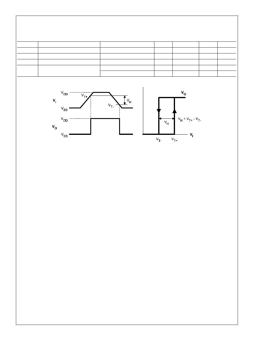
Schmitt Trigger
Symbol
Parameter
Conditions
Min
Typ
Max
Units
V
H
Hysteresis Voltage
V
T+
≠ V
T-
0.4
V
V
T-
Hysteresis Low Threshold Voltage
1.2
V
V
T+
Hysteresis High Threshold Voltage
1.6
V
I
INHYS
Input Current
V
IN
= V
DD
20
µA
V
IN
= V
SS
-20
0
µA
20101406
FIGURE 6. Hysteresis Definition
FPD87208AXA
www.national.com
5