Document Outline
- List of Figures
- List of Tables
- Table 2-1.� Pin Type Definitions
- Table 2-2.� 352 BGA Pin Assignments - Sorted by Pin Number
- Table 2-3.� 352 BGA Pin Assignments - Sorted Alphabetically by Signal Name
- Table 2-4.� 320 SPGA Pin Assignments - Sorted by Pin Number
- Table 2-5.� 320 SPGA Pin Assignments - Sorted Alphabetically by Signal Name
- Table 3-1.� Initialized Core Register Controls �
- Table 3-2.� Application Register Set
- Table 3-3.� Segment Register Selection Rules
- Table 3-4.� EFLAGS Register
- Table 3-5.� System Register Set
- Table 3-6.� Control Registers Map
- Table 3-7.� CR4-CR0 Bit Definitions �
- Table 3-8.� Effects of Various Combinations of EM, TS, and MP Bits
- Table 3-9.� Configuration Register Summary
- Table 3-10.� Configuration Register Map
- Table 3-11.� Configuration Registers �
- Table 3-12.� Debug Registers
- Table 3-13.� DR7 and DR6 Bit Definitions
- Table 3-14.� TLB Test Registers
- Table 3-15.� TR7-TR6 Bit Definitions �
- Table 3-16.� Cache Test Registers
- Table 3-17.� TR5-TR3 Bit Definitions
- Table 3-18.� Cache Test Operations
- Table 3-19.� Memory Addressing Modes
- Table 3-20.� GDTR, LDTR and IDTR Registers
- Table 3-21.� Application and System Segment Descriptors
- Table 3-22.� Application and System Segment Descriptors Bit Definitions �
- Table 3-23.� Application and System Segment Descriptors TYPE Bit Definitions �
- Table 3-24.� Gate Descriptors
- Table 3-25.� Gate Descriptors Bit Definitions
- Table 3-26.� 32-Bit Task State Segment (TSS) Table
- Table 3-27.� 16-Bit Task State Segment (TSS) Table
- Table 3-28.� Directory Table Entry (DTE) and Page Table Entry (PTE)
- Table 3-29.� Interrupt Vector Assignments
- Table 3-30.� Interrupt and Exception Priorities
- Table 3-31.� Exception Changes in Real Mode
- Table 3-32.� Error Codes
- Table 3-33.� Error Code Bit Definitions
- Table 3-34.� SMI# and SMINT Recognition Requirements
- Table 3-35.� SMM Memory Space Header
- Table 3-36.� SMM Memory Space Header Description
- Table 3-37.� SMM Instruction Set
- Table 3-38.� Descriptor Types Used for Control Transfer
- Table 3-39.� FPU Registers
- Table 4-1.� GCR Register
- Table 4-2.� Display Resolution Skip Counts
- Table 4-3.� L1 Cache BitBLT Register Summary
- Table 4-4.� L1 Cache BitBLT Registers
- Table 4-5.� Scratchpad Organization
- Table 4-6.� Display Driver Instructions
- Table 4-7.� CPU-Access Instructions
- Table 4-8.� Address Map for CPU-Access Registers
- Table 4-9.� Internal Bus Interface Unit Register Summary
- Table 4-10.� Internal Bus Interface Unit Registers�
- Table 4-11.� Region-Control-Field Bit Definitions
- Table 4-12.� Synchronous DRAM Configurations
- Table 4-13.� Basic Command Truth Table
- Table 4-14.� Address Line Programming during MRS Cycles
- Table 4-15.� Memory Controller Register Summary
- Table 4-16.� Memory Controller Registers �
- Table 4-17.� Auto LOI -- 2 DIMMs, Same Size, 1 DIMM Bank
- Table 4-18.� Auto LOI -- 2 DIMMs, Same Size, 2 DIMM Banks
- Table 4-19.� Non-Auto LOI -- 1 or 2 DIMMs, Different Sizes, 1 DIMM Bank
- Table 4-20.� Non-Auto LOI -- 1 or 2 DIMMs, Different Sizes, 2 DIMM Banks
- Table 4-21.� Graphics Pipeline Registers
- Table 4-22.� GP_RASTER_MODE Bit Patterns
- Table 4-23.� Common Raster Operations
- Table 4-24.� Graphics Pipeline Configuration Register Summary �
- Table 4-25.� Graphics Pipeline Configuration Registers �
- Table 4-26.� TFT Panel Display Modes
- Table 4-27.� TFT Panel Data Bus Formats
- Table 4-28.� CRT Display Modes
- Table 4-29.� Display Controller Register Summary �
- Table 4-30.� Display Controller Configuration and Status Registers �
- Table 4-31.� Display Controller Memory Organization Registers �
- Table 4-32.� Display Controller Timing Registers �
- Table 4-33.� Display Controller Cursor Position Registers �
- Table 4-34.� Display Controller Color Registers
- Table 4-35.� Display Controller Palette and RAM Diagnostic Registers�
- Table 4-36.� Special-Cycle Code to CONFIG_ADDRESS
- Table 4-37.� PCI Configuration Registers
- Table 4-38.� Format for Accessing the Internal PCI Configuration Registers
- Table 4-39.� PCI Configuration Space Register Summary
- Table 4-40.� PCI Configuration Registers �
- Table 5-1.� Standard VGA Modes
- Table 5-2.� VGA Configuration Registers Summary
- Table 5-3.� VGA Configuration Registers
- Table 5-4.� Virtual VGA Register Summary
- Table 5-5.� Virtual VGA Registers
- Table 6-1.� Power Management Register Summary �
- Table 6-2.� Power Management Control and Status Registers �
- Table 6-3.� Power Management Programmable Address Region Registers
- Table 7-1.� Part Numbers
- Table 7-2.� Pins with 20-kohm Internal Resistor
- Table 7-3.� Absolute Maximum Ratings
- Table 7-4.� Operating Conditions
- Table 7-5.� DC Characteristics
- Table 7-6.� Drive Level and Measurement Points for Switching Characteristics
- Table 7-7.� Clock Signals
- Table 7-8.� System Signals
- Table 7-9.� PCI Interface Signals
- Table 7-10.� SDRAM Interface Signals
- Table 7-11.� Video Interface Signals
- Table 7-12.� JTAG AC Specification
- Table 8-1.� Junction-to-Case Thermal Resistance for SPGA and BGA Packages
- Table 8-2.� Case-to-Ambient Thermal Resistance Examples @ 85�C
- Table 8-3.� Mechanical Package Outline Legend
- Table 9-1.� General Instruction Set Format
- Table 9-2.� Instruction Fields
- Table 9-3.� Instruction Prefix Summary
- Table 9-4.� w Field Encoding
- Table 9-5.� d Field Encoding
- Table 9-6.� s Field Encoding
- Table 9-7.� eee Field Encoding
- Table 9-8.� General Registers Selected by mod r/m Fields and w Field
- Table 9-9.� mod r/m Field Encoding
- Table 9-10.� General Registers Selected by reg Field
- Table 9-11.� sreg2 Field Encoding
- Table 9-12.� sreg3 Field Encoding
- Table 9-13.� ss Field Encoding
- Table 9-14.� index Field Encoding
- Table 9-15.� mod base Field Encoding
- Table 9-16.� CPUID Levels Summary
- Table 9-17.� CPUID Data Returned when EAX = 0
- Table 9-18.� EAX, EBX, ECX CPUID Data Returned when EAX = 1
- Table 9-19.� EDX CPUID Data Returned when EAX = 1�
- Table 9-20.� Standard CPUID with EAX = 00000002h
- Table 9-21.� Maximum Extended CPUID Level
- Table 9-22.� EAX, EBX, ECX CPUID Data Returned when EAX = 80000001h
- Table 9-23.� EDX CPUID Data Returned when EAX = 80000001h
- Table 9-24.� Official CPU Name
- Table 9-25.� Standard CPUID with EAX = 80000005h
- Table 9-26.� Processor Core Instruction Set Table Legend
- Table 9-27.� Processor Core Instruction Set Summary �
- Table 9-28.� FPU Instruction Set Table Legend
- Table 9-29.� FPU Instruction Set Summary �
- Table 9-30.� MMX Instruction Set Table Legend
- Table 9-31.� MMX Instruction Set Summary �
- Table 9-32.� Extend MMX Instruction Set Table Legend
- Table 9-33.� Extended MMX Instruction Set Summary �
- Table A-1.� Revision History
- Table A-2.� Edits to Current Revision
- 1.0 Architecture Overview
- 2.0 Signal Definitions
- 3.0 Processor Programming
- 4.0 Integrated Functions
- 5.0 Virtual Subsystem Architecture
- 6.0 Power Management
- 7.0 Electrical Specifications
- 8.0 Package Specifications
- 9.0 Instruction Set
- Appendix A Support Documentation
© 2000 National Semiconductor Corporation
www.national.com
GeodeTM
G
Xm
P
r
ocessor
I
ntegrated
x
86
S
o
l
u
t
i
o
n
with
M
M
X
Suppor
t
April 2000
GeodeTM GXm Processor
Integrated x86 Solution with MMX Support
General Description
The National Semiconductor
Æ
GeodeTM GXm processor
is an advanced 32-bit x86 compatible processor offering
high performance, fully accelerated 2D graphics, a 64-bit
synchronous DRAM controller and a PCI bus controller,
all on a single chip that is compatible with Intel's MMX
technology.
The GXm processor core is a proven design that offers
competitive CPU performance. It has integer and floating
point execution units that are based on sixth-generation
technology. The integer core contains a single, six-stage
execution pipeline and offers advanced features such as
operand forwarding, branch target buffers, and extensive
write buffering. A 16 KB write-back L1 cache is accessed
in a unique fashion that eliminates pipeline stalls to fetch
operands that hit in the cache.
In addition to the advanced CPU features, the GXm pro-
cessor integrates a host of functions which are typically
implemented with external components. A full-function
graphics accelerator provides pixel processing and ren-
dering functions.
A separate on-chip video buffer enables >30 fps MPEG1
video playback when used together with the CS5530 I/O
companion chip. Graphics and system memory accesses
are supported by a tightly-coupled synchronous DRAM
(SDRAM) memory controller. This tightly coupled memory
subsystem eliminates the need for an external L2 cache.
The GXm processor includes Virtual System Architec-
ture
Æ
(VSATM technology) enabling XpressGRAPHICS
and XpressAUDIO subsystems as well as generic emula-
tion capabilities. Software handler routines for the Xpress-
GRAPHICS and XpressAUDIO subsystems can be
included in the BIOS and provide compatible VGA and 16-
bit industry standard audio emulation. XpressAUDIO tech-
nology eliminates much of the hardware traditionally asso-
ciated with audio functions.
GeodeTM GXm Processor Internal Block Diagram
Write-Back
Unit
FPU
Internal Bus Interface Unit
Graphics
Memory
Display
PCI
SDRAM Port
CS5530
PCI Bus
Integer
Cache Unit
Integrated
Functions
MMU
(CRT/LCD TFT)
X-Bus
Pipeline
Controller
Controller
Controller
C-Bus
National Semiconductor and Virtual System Architecture are registered trademarks of National Semiconductor Corporation.
Geode and VSA are trademarks of National Semiconductor Corporation.
For a complete listing of National Semiconductor trademarks, please visit www.national.com/trademarks.

www.national.com
2
Revision 3.1
GeodeTM
G
Xm
Pr
ocessor
Features
General Features
Packaged in:
-- 352-Terminal Ball Grid Array (BGA) or
-- 320-Pin Staggered Pin Grid Array (SPGA)
0.35-micron four layer metal CMOS process
Split rail design (3.3V I/O and 2.9V core)
32-Bit x86 Processor
Supports the MMX instruction set extension for the
acceleration of multimedia applications
Speeds offered up to 266 MHz
16 KB unified L1 cache
Integrated Floating Point Unit (FPU)
Re-entrant System Management Mode (SMM)
enhanced for VSA
PCI Controller
Fixed, rotating, hybrid, or ping-pong arbitration
Supports up to three PCI bus masters
Synchronous CPU and PCI bus clock frequency
Supports concurrency between PCI master and L1
cache
Power Management
Designed to support CS5530 power management
architecture
CPU only Suspend or full 3V Suspend supported:
-- Clocks to CPU core stopped for CPU Suspend
-- All on-chip clocks stopped for 3V Suspend
-- Suspend refresh supported for 3V Suspend
Virtual Systems Architecture Technology
Architecture allows OS independent (software) virtual-
ization of hardware functions
Provides compatible high performance legacy VGA
core functionality
Note: GUI (Graphical User Interface) graphics accel-
eration is pure hardware.
Provides 16-bit XpressAUDIO subsystem
2D Graphics Accelerator
Graphics pipeline performance significantly increased
over previous generations by pipelining burst
reads/writes
Accelerates BitBLTs, line draw, text
Supports all 256 raster operations
Supports transparent BLTs
Runs at core clock frequency
Full VGA and VESA mode support
Special "Driver level" instructions utilize internal
scratchpad for enhanced performance
Display Controller
Video Generator (VG) improves memory efficiency for
display refresh with SDRAM
Supports a separate MPEG1 video buffer and data
path to enable video acceleration in the CS5530
Internal palette RAM for use with the CS5530
Direct interface to CS5530 for CRT and TFT flat panel
support which eliminates need for external RAMDAC
Hardware frame buffer compressor/decompressor
Hardware cursor
Supports up to 1280x1024x8 bpp and 1024x768x16
bpp
XpressRAM Subsystem
Memory control/interface directly from CPU
64-Bit wide memory bus
Support for:
-- Two 168-pin unbuffered DIMMs
-- Up to 16 open banks simultaneously
-- Single or 16-byte reads (burst length of two)

Revision 3.1
3
www.national.com
Table of Contents
GeodeTM
G
Xm
P
r
ocessor
1.0
Architecture Overview . . . . . . . . . . . . . . . . . . . . . . . . . . . . . . . . . . . . . . . . . . . . . 8
1.1
INTEGER UNIT . . . . . . . . . . . . . . . . . . . . . . . . . . . . . . . . . . . . . . . . . . . . . . . . . . . . . . . . . . . 8
1.2
FLOATING POINT UNIT . . . . . . . . . . . . . . . . . . . . . . . . . . . . . . . . . . . . . . . . . . . . . . . . . . . . 9
1.3
WRITE-BACK CACHE UNIT . . . . . . . . . . . . . . . . . . . . . . . . . . . . . . . . . . . . . . . . . . . . . . . . . 9
1.4
MEMORY MANAGEMENT UNIT . . . . . . . . . . . . . . . . . . . . . . . . . . . . . . . . . . . . . . . . . . . . . . 9
1.4.1
Internal Bus Interface Unit . . . . . . . . . . . . . . . . . . . . . . . . . . . . . . . . . . . . . . . . . . . . 9
1.5
INTEGRATED FUNCTIONS . . . . . . . . . . . . . . . . . . . . . . . . . . . . . . . . . . . . . . . . . . . . . . . . . 9
1.5.1
Graphics Accelerator . . . . . . . . . . . . . . . . . . . . . . . . . . . . . . . . . . . . . . . . . . . . . . . . 9
1.5.2
Display Controller . . . . . . . . . . . . . . . . . . . . . . . . . . . . . . . . . . . . . . . . . . . . . . . . . . 10
1.5.3
XpressRAM Memory Subsystem . . . . . . . . . . . . . . . . . . . . . . . . . . . . . . . . . . . . . . 10
1.5.4
PCI Controller . . . . . . . . . . . . . . . . . . . . . . . . . . . . . . . . . . . . . . . . . . . . . . . . . . . . . 10
1.6
GEODE GXM/CS5530 SYSTEM DESIGNS . . . . . . . . . . . . . . . . . . . . . . . . . . . . . . . . . . . . 11
2.0
Signal Definitions . . . . . . . . . . . . . . . . . . . . . . . . . . . . . . . . . . . . . . . . . . . . . . . . 13
2.1
PIN ASSIGNMENTS . . . . . . . . . . . . . . . . . . . . . . . . . . . . . . . . . . . . . . . . . . . . . . . . . . . . . . 13
2.2
SIGNAL DESCRIPTIONS . . . . . . . . . . . . . . . . . . . . . . . . . . . . . . . . . . . . . . . . . . . . . . . . . . 24
2.2.1
System Interface Signals . . . . . . . . . . . . . . . . . . . . . . . . . . . . . . . . . . . . . . . . . . . . 24
2.2.2
PCI Interface Signals . . . . . . . . . . . . . . . . . . . . . . . . . . . . . . . . . . . . . . . . . . . . . . . 26
2.2.3
Memory Controller Interface Signals . . . . . . . . . . . . . . . . . . . . . . . . . . . . . . . . . . . 29
2.2.4
Video Interface Signals . . . . . . . . . . . . . . . . . . . . . . . . . . . . . . . . . . . . . . . . . . . . . 30
2.2.5
Power, Ground, and No Connect Signals . . . . . . . . . . . . . . . . . . . . . . . . . . . . . . . . 32
2.2.6
Internal Test and Measurement Signals . . . . . . . . . . . . . . . . . . . . . . . . . . . . . . . . 32
2.3
SUBSYSTEM SIGNAL CONNECTIONS . . . . . . . . . . . . . . . . . . . . . . . . . . . . . . . . . . . . . . . 34
2.4
POWER PLANES . . . . . . . . . . . . . . . . . . . . . . . . . . . . . . . . . . . . . . . . . . . . . . . . . . . . . . . . . 36
3.0
Processor Programming . . . . . . . . . . . . . . . . . . . . . . . . . . . . . . . . . . . . . . . . . . 38
3.1
CORE PROCESSOR INITIALIZATION . . . . . . . . . . . . . . . . . . . . . . . . . . . . . . . . . . . . . . . . 38
3.2
INSTRUCTION SET OVERVIEW . . . . . . . . . . . . . . . . . . . . . . . . . . . . . . . . . . . . . . . . . . . . . 39
3.2.1
Lock Prefix . . . . . . . . . . . . . . . . . . . . . . . . . . . . . . . . . . . . . . . . . . . . . . . . . . . . . . . 39
3.3
REGISTER SETS . . . . . . . . . . . . . . . . . . . . . . . . . . . . . . . . . . . . . . . . . . . . . . . . . . . . . . . . . 40
3.3.1
Application Register Set . . . . . . . . . . . . . . . . . . . . . . . . . . . . . . . . . . . . . . . . . . . . . 40
3.3.2
System Register Set . . . . . . . . . . . . . . . . . . . . . . . . . . . . . . . . . . . . . . . . . . . . . . . 44
3.3.3
Model Specific Register Set . . . . . . . . . . . . . . . . . . . . . . . . . . . . . . . . . . . . . . . . . . 59
3.3.4
Time Stamp Counter . . . . . . . . . . . . . . . . . . . . . . . . . . . . . . . . . . . . . . . . . . . . . . . 59
3.4
ADDRESS SPACES . . . . . . . . . . . . . . . . . . . . . . . . . . . . . . . . . . . . . . . . . . . . . . . . . . . . . . . 60
3.4.1
I/O Address Space . . . . . . . . . . . . . . . . . . . . . . . . . . . . . . . . . . . . . . . . . . . . . . . . . 60
3.4.2
Memory Address Space . . . . . . . . . . . . . . . . . . . . . . . . . . . . . . . . . . . . . . . . . . . . . 60
3.5
OFFSET, SEGMENT, AND PAGING MECHANISMS . . . . . . . . . . . . . . . . . . . . . . . . . . . . . 61
3.6
OFFSET MECHANISM . . . . . . . . . . . . . . . . . . . . . . . . . . . . . . . . . . . . . . . . . . . . . . . . . . . . 61
3.7
DESCRIPTORS AND SEGMENT MECHANISMS . . . . . . . . . . . . . . . . . . . . . . . . . . . . . . . . 62
3.7.1
Real and Virtual 8086 Mode Segment Mechanisms . . . . . . . . . . . . . . . . . . . . . . . 62
3.7.2
Segment Mechanism in Protective Mode . . . . . . . . . . . . . . . . . . . . . . . . . . . . . . . . 63
3.7.3
GDTR and LDTR Registers . . . . . . . . . . . . . . . . . . . . . . . . . . . . . . . . . . . . . . . . . . 66
3.7.4
Descriptor Bit Structure . . . . . . . . . . . . . . . . . . . . . . . . . . . . . . . . . . . . . . . . . . . . . 67
3.7.5
Gate Descriptors . . . . . . . . . . . . . . . . . . . . . . . . . . . . . . . . . . . . . . . . . . . . . . . . . . 69
3.8
MULTITASKING AND TASK STATE SEGMENTS . . . . . . . . . . . . . . . . . . . . . . . . . . . . . . . . 70
3.9
PAGING MECHANISM . . . . . . . . . . . . . . . . . . . . . . . . . . . . . . . . . . . . . . . . . . . . . . . . . . . . . 72

www.national.com
4
Revision 3.1
Table of Contents
(Continued)
GeodeTM
G
Xm
Pr
ocessor
3.10
INTERRUPTS AND EXCEPTIONS . . . . . . . . . . . . . . . . . . . . . . . . . . . . . . . . . . . . . . . . . . . 74
3.10.1
Interrupts . . . . . . . . . . . . . . . . . . . . . . . . . . . . . . . . . . . . . . . . . . . . . . . . . . . . . . . . 74
3.10.2
Exceptions . . . . . . . . . . . . . . . . . . . . . . . . . . . . . . . . . . . . . . . . . . . . . . . . . . . . . . . 74
3.10.3
Interrupt Vectors . . . . . . . . . . . . . . . . . . . . . . . . . . . . . . . . . . . . . . . . . . . . . . . . . . . 75
3.10.4
Interrupt and Exception Priorities . . . . . . . . . . . . . . . . . . . . . . . . . . . . . . . . . . . . . . 76
3.10.5
Exceptions in Real Mode . . . . . . . . . . . . . . . . . . . . . . . . . . . . . . . . . . . . . . . . . . . . 77
3.10.6
Error Codes . . . . . . . . . . . . . . . . . . . . . . . . . . . . . . . . . . . . . . . . . . . . . . . . . . . . . . 77
3.11
SYSTEM MANAGEMENT MODE . . . . . . . . . . . . . . . . . . . . . . . . . . . . . . . . . . . . . . . . . . . . 78
3.11.1
SMM Enhancements . . . . . . . . . . . . . . . . . . . . . . . . . . . . . . . . . . . . . . . . . . . . . . . 79
3.11.2
SMM Operation . . . . . . . . . . . . . . . . . . . . . . . . . . . . . . . . . . . . . . . . . . . . . . . . . . . 79
3.11.3
The SMI# Pin . . . . . . . . . . . . . . . . . . . . . . . . . . . . . . . . . . . . . . . . . . . . . . . . . . . . . 80
3.11.4
SMM Configuration Registers . . . . . . . . . . . . . . . . . . . . . . . . . . . . . . . . . . . . . . . . 80
3.11.5
SMM Memory Space Header . . . . . . . . . . . . . . . . . . . . . . . . . . . . . . . . . . . . . . . . . 80
3.11.6
SMM Instructions . . . . . . . . . . . . . . . . . . . . . . . . . . . . . . . . . . . . . . . . . . . . . . . . . . 82
3.11.7
SMM Memory Space . . . . . . . . . . . . . . . . . . . . . . . . . . . . . . . . . . . . . . . . . . . . . . . 83
3.11.8
SMI Generation . . . . . . . . . . . . . . . . . . . . . . . . . . . . . . . . . . . . . . . . . . . . . . . . . . . 83
3.11.9
SMI Service Routine Execution . . . . . . . . . . . . . . . . . . . . . . . . . . . . . . . . . . . . . . . 83
3.12
SHUTDOWN AND HALT . . . . . . . . . . . . . . . . . . . . . . . . . . . . . . . . . . . . . . . . . . . . . . . . . . . 86
3.13
PROTECTION . . . . . . . . . . . . . . . . . . . . . . . . . . . . . . . . . . . . . . . . . . . . . . . . . . . . . . . . . . . 86
3.13.1
Privilege Levels . . . . . . . . . . . . . . . . . . . . . . . . . . . . . . . . . . . . . . . . . . . . . . . . . . . 86
3.13.2
I/O Privilege Levels . . . . . . . . . . . . . . . . . . . . . . . . . . . . . . . . . . . . . . . . . . . . . . . . 86
3.13.3
Privilege Level Transfers . . . . . . . . . . . . . . . . . . . . . . . . . . . . . . . . . . . . . . . . . . . . 87
3.13.4
Initialization and Transition to Protected Mode . . . . . . . . . . . . . . . . . . . . . . . . . . . . 87
3.14
VIRTUAL 8086 MODE . . . . . . . . . . . . . . . . . . . . . . . . . . . . . . . . . . . . . . . . . . . . . . . . . . . . . 88
3.14.1
Memory Addressing . . . . . . . . . . . . . . . . . . . . . . . . . . . . . . . . . . . . . . . . . . . . . . . . 88
3.14.2
Protection . . . . . . . . . . . . . . . . . . . . . . . . . . . . . . . . . . . . . . . . . . . . . . . . . . . . . . . . 88
3.14.3
Interrupt Handling . . . . . . . . . . . . . . . . . . . . . . . . . . . . . . . . . . . . . . . . . . . . . . . . . . 88
3.14.4
Entering and Leaving Virtual 8086 Mode . . . . . . . . . . . . . . . . . . . . . . . . . . . . . . . . 88
3.15
FLOATING POINT UNIT OPERATIONS . . . . . . . . . . . . . . . . . . . . . . . . . . . . . . . . . . . . . . . 89
3.15.1
FPU (Floating Point Unit) Register Set . . . . . . . . . . . . . . . . . . . . . . . . . . . . . . . . . . 89
3.15.2
FPU Tag Word Register . . . . . . . . . . . . . . . . . . . . . . . . . . . . . . . . . . . . . . . . . . . . . 89
3.15.3
FPU Status Register . . . . . . . . . . . . . . . . . . . . . . . . . . . . . . . . . . . . . . . . . . . . . . . 89
3.15.4
FPU Mode Control Register . . . . . . . . . . . . . . . . . . . . . . . . . . . . . . . . . . . . . . . . . . 89
4.0
Integrated Functions . . . . . . . . . . . . . . . . . . . . . . . . . . . . . . . . . . . . . . . . . . . . . 91
4.1
INTEGRATED FUNCTIONS PROGRAMMING INTERFACE . . . . . . . . . . . . . . . . . . . . . . . 92
4.1.1
Graphics Control Register . . . . . . . . . . . . . . . . . . . . . . . . . . . . . . . . . . . . . . . . . . . 92
4.1.2
Control Registers . . . . . . . . . . . . . . . . . . . . . . . . . . . . . . . . . . . . . . . . . . . . . . . . . . 94
4.1.3
Graphics Memory . . . . . . . . . . . . . . . . . . . . . . . . . . . . . . . . . . . . . . . . . . . . . . . . . . 94
4.1.4
L1 Cache Controller . . . . . . . . . . . . . . . . . . . . . . . . . . . . . . . . . . . . . . . . . . . . . . . . 95
4.1.5
Display Driver Instructions . . . . . . . . . . . . . . . . . . . . . . . . . . . . . . . . . . . . . . . . . . . 98
4.1.6
CPU_READ/CPU_WRITE Instructions . . . . . . . . . . . . . . . . . . . . . . . . . . . . . . . . . 99
4.2
INTERNAL BUS INTERFACE UNIT . . . . . . . . . . . . . . . . . . . . . . . . . . . . . . . . . . . . . . . . . . 100
4.2.1
FPU Error Support . . . . . . . . . . . . . . . . . . . . . . . . . . . . . . . . . . . . . . . . . . . . . . . . 100
4.2.2
A20M Support . . . . . . . . . . . . . . . . . . . . . . . . . . . . . . . . . . . . . . . . . . . . . . . . . . . 100
4.2.3
SMI Generation . . . . . . . . . . . . . . . . . . . . . . . . . . . . . . . . . . . . . . . . . . . . . . . . . . 100
4.2.4
640 KB to 1 MB Region . . . . . . . . . . . . . . . . . . . . . . . . . . . . . . . . . . . . . . . . . . . . 100
4.2.5
Internal Bus Interface Unit Registers . . . . . . . . . . . . . . . . . . . . . . . . . . . . . . . . . . 101

Revision 3.1
5
www.national.com
Table of Contents
(Continued)
GeodeTM
G
Xm
P
r
ocessor
4.3
MEMORY CONTROLLER . . . . . . . . . . . . . . . . . . . . . . . . . . . . . . . . . . . . . . . . . . . . . . . . . 103
4.3.1
Memory Array Configuration . . . . . . . . . . . . . . . . . . . . . . . . . . . . . . . . . . . . . . . . 104
4.3.2
Memory Organizations . . . . . . . . . . . . . . . . . . . . . . . . . . . . . . . . . . . . . . . . . . . . . 105
4.3.3
SDRAM Commands . . . . . . . . . . . . . . . . . . . . . . . . . . . . . . . . . . . . . . . . . . . . . . . 106
4.3.4
Memory Controller Register Description . . . . . . . . . . . . . . . . . . . . . . . . . . . . . . . 108
4.3.5
Address Translation . . . . . . . . . . . . . . . . . . . . . . . . . . . . . . . . . . . . . . . . . . . . . . . 112
4.3.6
Memory Cycles . . . . . . . . . . . . . . . . . . . . . . . . . . . . . . . . . . . . . . . . . . . . . . . . . . 115
4.3.7
SDRAM Interface Clocking . . . . . . . . . . . . . . . . . . . . . . . . . . . . . . . . . . . . . . . . . . 118
4.4
GRAPHICS PIPELINE . . . . . . . . . . . . . . . . . . . . . . . . . . . . . . . . . . . . . . . . . . . . . . . . . . . . 120
4.4.1
BitBLT/Vector Engine . . . . . . . . . . . . . . . . . . . . . . . . . . . . . . . . . . . . . . . . . . . . . . 120
4.4.2
Master/Slave Registers . . . . . . . . . . . . . . . . . . . . . . . . . . . . . . . . . . . . . . . . . . . . 121
4.4.3
Pattern Generation . . . . . . . . . . . . . . . . . . . . . . . . . . . . . . . . . . . . . . . . . . . . . . . . 121
4.4.4
Source Expansion . . . . . . . . . . . . . . . . . . . . . . . . . . . . . . . . . . . . . . . . . . . . . . . . 123
4.4.5
Raster Operations . . . . . . . . . . . . . . . . . . . . . . . . . . . . . . . . . . . . . . . . . . . . . . . . 123
4.4.6
Graphics Pipeline Register Descriptions . . . . . . . . . . . . . . . . . . . . . . . . . . . . . . . 124
4.5
DISPLAY CONTROLLER . . . . . . . . . . . . . . . . . . . . . . . . . . . . . . . . . . . . . . . . . . . . . . . . . . 129
4.5.1
Display FIFO . . . . . . . . . . . . . . . . . . . . . . . . . . . . . . . . . . . . . . . . . . . . . . . . . . . . 130
4.5.2
Compression Technology . . . . . . . . . . . . . . . . . . . . . . . . . . . . . . . . . . . . . . . . . . . 130
4.5.3
Motion Video Acceleration Support . . . . . . . . . . . . . . . . . . . . . . . . . . . . . . . . . . . 130
4.5.4
Hardware Cursor . . . . . . . . . . . . . . . . . . . . . . . . . . . . . . . . . . . . . . . . . . . . . . . . . 131
4.5.5
Display Timing Generator . . . . . . . . . . . . . . . . . . . . . . . . . . . . . . . . . . . . . . . . . . . 131
4.5.6
Dither and Frame-Rate Modulation . . . . . . . . . . . . . . . . . . . . . . . . . . . . . . . . . . . 131
4.5.7
Display Modes . . . . . . . . . . . . . . . . . . . . . . . . . . . . . . . . . . . . . . . . . . . . . . . . . . . 131
4.5.8
Graphics Memory Map . . . . . . . . . . . . . . . . . . . . . . . . . . . . . . . . . . . . . . . . . . . . . 135
4.5.9
Display Controller Registers . . . . . . . . . . . . . . . . . . . . . . . . . . . . . . . . . . . . . . . . . 136
4.5.10
Memory Organization Registers . . . . . . . . . . . . . . . . . . . . . . . . . . . . . . . . . . . . . . 144
4.5.11
Timing Registers . . . . . . . . . . . . . . . . . . . . . . . . . . . . . . . . . . . . . . . . . . . . . . . . . 146
4.5.12
Cursor Position Registers . . . . . . . . . . . . . . . . . . . . . . . . . . . . . . . . . . . . . . . . . . . 149
4.5.13
Color Registers . . . . . . . . . . . . . . . . . . . . . . . . . . . . . . . . . . . . . . . . . . . . . . . . . . 150
4.5.14
Palette Access Registers . . . . . . . . . . . . . . . . . . . . . . . . . . . . . . . . . . . . . . . . . . . 151
4.5.15
CS5530 Display Controller Interface . . . . . . . . . . . . . . . . . . . . . . . . . . . . . . . . . . 153
4.6
PCI CONTROLLER . . . . . . . . . . . . . . . . . . . . . . . . . . . . . . . . . . . . . . . . . . . . . . . . . . . . . . 155
4.6.1
X-Bus PCI Slave . . . . . . . . . . . . . . . . . . . . . . . . . . . . . . . . . . . . . . . . . . . . . . . . . . 155
4.6.2
X-Bus PCI Master . . . . . . . . . . . . . . . . . . . . . . . . . . . . . . . . . . . . . . . . . . . . . . . . 155
4.6.3
PCI Arbiter . . . . . . . . . . . . . . . . . . . . . . . . . . . . . . . . . . . . . . . . . . . . . . . . . . . . . . 155
4.6.4
Generating Configuration Cycles . . . . . . . . . . . . . . . . . . . . . . . . . . . . . . . . . . . . . 155
4.6.5
Generating Special Cycles . . . . . . . . . . . . . . . . . . . . . . . . . . . . . . . . . . . . . . . . . . 155
4.6.6
PCI Configuration Space Control Registers . . . . . . . . . . . . . . . . . . . . . . . . . . . . . 156
4.6.7
PCI Configuration Space Registers . . . . . . . . . . . . . . . . . . . . . . . . . . . . . . . . . . . 157
4.6.8
PCI Cycles . . . . . . . . . . . . . . . . . . . . . . . . . . . . . . . . . . . . . . . . . . . . . . . . . . . . . . 162
5.0
Virtual Subsystem Architecture . . . . . . . . . . . . . . . . . . . . . . . . . . . . . . . . . . . 165
5.1
VIRTUAL VGA . . . . . . . . . . . . . . . . . . . . . . . . . . . . . . . . . . . . . . . . . . . . . . . . . . . . . . . . . . 165
5.1.1
Traditional VGA Hardware . . . . . . . . . . . . . . . . . . . . . . . . . . . . . . . . . . . . . . . . . . 165
5.2
GXM VIRTUAL VGA . . . . . . . . . . . . . . . . . . . . . . . . . . . . . . . . . . . . . . . . . . . . . . . . . . . . . . 167
5.2.1
Datapath Elements . . . . . . . . . . . . . . . . . . . . . . . . . . . . . . . . . . . . . . . . . . . . . . . . 167
5.2.2
Video Refresh . . . . . . . . . . . . . . . . . . . . . . . . . . . . . . . . . . . . . . . . . . . . . . . . . . . 168
5.2.3
GXm VGA Hardware . . . . . . . . . . . . . . . . . . . . . . . . . . . . . . . . . . . . . . . . . . . . . . 168
5.2.4
VGA Video BIOS . . . . . . . . . . . . . . . . . . . . . . . . . . . . . . . . . . . . . . . . . . . . . . . . . 171
5.2.5
Virtual VGA Register Descriptions . . . . . . . . . . . . . . . . . . . . . . . . . . . . . . . . . . . . 172

www.national.com
6
Revision 3.1
Table of Contents
(Continued)
GeodeTM
G
Xm
Pr
ocessor
6.0
Power Management . . . . . . . . . . . . . . . . . . . . . . . . . . . . . . . . . . . . . . . . . . . . . 174
6.1
APM SUPPORT . . . . . . . . . . . . . . . . . . . . . . . . . . . . . . . . . . . . . . . . . . . . . . . . . . . . . . . . . 174
6.2
CPU SUSPEND COMMAND REGISTERS . . . . . . . . . . . . . . . . . . . . . . . . . . . . . . . . . . . . 174
6.3
SUSPEND MODULATION . . . . . . . . . . . . . . . . . . . . . . . . . . . . . . . . . . . . . . . . . . . . . . . . . 174
6.4
3-VOLT SUSPEND MODE . . . . . . . . . . . . . . . . . . . . . . . . . . . . . . . . . . . . . . . . . . . . . . . . . 174
6.5
SUSPEND MODE AND BUS CYCLES . . . . . . . . . . . . . . . . . . . . . . . . . . . . . . . . . . . . . . . 175
6.5.1
Initiating Suspend with SUSP# . . . . . . . . . . . . . . . . . . . . . . . . . . . . . . . . . . . . . . 175
6.5.2
Initiating Suspend with HALT . . . . . . . . . . . . . . . . . . . . . . . . . . . . . . . . . . . . . . . . 176
6.5.3
Responding to a PCI Access During Suspend Mode . . . . . . . . . . . . . . . . . . . . . . 177
6.5.4
Stopping the Input Clock . . . . . . . . . . . . . . . . . . . . . . . . . . . . . . . . . . . . . . . . . . . 178
6.6
GXM PROCESSOR SERIAL BUS . . . . . . . . . . . . . . . . . . . . . . . . . . . . . . . . . . . . . . . . . . 179
6.6.1
Serial Packet Transmission . . . . . . . . . . . . . . . . . . . . . . . . . . . . . . . . . . . . . . . . . 179
6.7
POWER MANAGEMENT REGISTERS . . . . . . . . . . . . . . . . . . . . . . . . . . . . . . . . . . . . . . . 179
7.0
Electrical Specifications. . . . . . . . . . . . . . . . . . . . . . . . . . . . . . . . . . . . . . . . . . 182
7.1
PART NUMBERS . . . . . . . . . . . . . . . . . . . . . . . . . . . . . . . . . . . . . . . . . . . . . . . . . . . . . . . . 182
7.2
ELECTRICAL CONNECTIONS . . . . . . . . . . . . . . . . . . . . . . . . . . . . . . . . . . . . . . . . . . . . . 182
7.2.1
Power/Ground Connections and Decoupling . . . . . . . . . . . . . . . . . . . . . . . . . . . . 182
7.2.2
Power Sequencing the Core and I/O Voltages . . . . . . . . . . . . . . . . . . . . . . . . . . . 182
7.2.3
NC-Designated Pins . . . . . . . . . . . . . . . . . . . . . . . . . . . . . . . . . . . . . . . . . . . . . . . 182
7.2.4
Pull-Up and Pull-Down Resistors . . . . . . . . . . . . . . . . . . . . . . . . . . . . . . . . . . . . . 182
7.2.5
Unused Input Pins . . . . . . . . . . . . . . . . . . . . . . . . . . . . . . . . . . . . . . . . . . . . . . . . 182
7.3
ABSOLUTE MAXIMUM RATINGS . . . . . . . . . . . . . . . . . . . . . . . . . . . . . . . . . . . . . . . . . . . 183
7.4
OPERATING CONDITIONS . . . . . . . . . . . . . . . . . . . . . . . . . . . . . . . . . . . . . . . . . . . . . . . . 184
7.5
DC CHARACTERISTICS . . . . . . . . . . . . . . . . . . . . . . . . . . . . . . . . . . . . . . . . . . . . . . . . . . 185
7.6
AC CHARACTERISTICS . . . . . . . . . . . . . . . . . . . . . . . . . . . . . . . . . . . . . . . . . . . . . . . . . . 186
8.0
Package Specifications . . . . . . . . . . . . . . . . . . . . . . . . . . . . . . . . . . . . . . . . . . 195
8.1
THERMAL CHARACTERISTICS . . . . . . . . . . . . . . . . . . . . . . . . . . . . . . . . . . . . . . . . . . . . 195
8.1.1
Heatsink Considerations . . . . . . . . . . . . . . . . . . . . . . . . . . . . . . . . . . . . . . . . . . . 196
8.2
MECHANICAL PACKAGE OUTLINES . . . . . . . . . . . . . . . . . . . . . . . . . . . . . . . . . . . . . . . . 198
9.0
Instruction Set. . . . . . . . . . . . . . . . . . . . . . . . . . . . . . . . . . . . . . . . . . . . . . . . . . 201
9.1
GENERAL INSTRUCTION SET FORMAT . . . . . . . . . . . . . . . . . . . . . . . . . . . . . . . . . . . . . 202
9.1.1
Prefix (Optional)
. . . . . . . . . . . . . . . . . . . . . . . . . . . . . . . . . . . . . . . . . . . . . . . . . 203
9.1.2
Opcode . . . . . . . . . . . . . . . . . . . . . . . . . . . . . . . . . . . . . . . . . . . . . . . . . . . . . . . . . 203
9.1.3
mod and r/m Byte (Memory Addressing) . . . . . . . . . . . . . . . . . . . . . . . . . . . . . . . 205
9.1.4
reg Field . . . . . . . . . . . . . . . . . . . . . . . . . . . . . . . . . . . . . . . . . . . . . . . . . . . . . . . . 206
9.1.5
s-i-b Byte (Scale, Indexing, Base) . . . . . . . . . . . . . . . . . . . . . . . . . . . . . . . . . . . . 207
9.2
CPUID INSTRUCTION . . . . . . . . . . . . . . . . . . . . . . . . . . . . . . . . . . . . . . . . . . . . . . . . . . . . 208
9.2.1
Standard CPUID Levels . . . . . . . . . . . . . . . . . . . . . . . . . . . . . . . . . . . . . . . . . . . . 208
9.2.2
Extended CPUID Levels . . . . . . . . . . . . . . . . . . . . . . . . . . . . . . . . . . . . . . . . . . . . 210
9.3
PROCESSOR CORE INSTRUCTION SET . . . . . . . . . . . . . . . . . . . . . . . . . . . . . . . . . . . . 212
9.4
FPU INSTRUCTION SET . . . . . . . . . . . . . . . . . . . . . . . . . . . . . . . . . . . . . . . . . . . . . . . . . . 224
9.5
MMX INSTRUCTION SET . . . . . . . . . . . . . . . . . . . . . . . . . . . . . . . . . . . . . . . . . . . . . . . . . 229
9.6
NATIONAL SEMICONDUCTOR EXTENDED MMX INSTRUCTION SET . . . . . . . . . . . . . 234

Revision 3.1
7
www.national.com
Table of Contents
(Continued)
GeodeTM
G
Xm
P
r
ocessor
Appendix A Support Documentation . . . . . . . . . . . . . . . . . . . . . . . . . . . . . . . . . . . . . 236
A.1
ORDER INFORMATION . . . . . . . . . . . . . . . . . . . . . . . . . . . . . . . . . . . . . . . . . . . . . . . . . . 236
A.2
DATA BOOK REVISION HISTORY . . . . . . . . . . . . . . . . . . . . . . . . . . . . . . . . . . . . . . . . . . 236

www.national.com
8
Revision 3.1
GeodeTM
G
Xm
Pr
ocessor
1.0
Architecture Overview
The National Semiconductor Geode GXm processor is
an x86-compatible 32-bit microprocessor. The decoupled
load/store unit (within the memory management unit)
allows multiple instructions in a single clock cycle. Other
features
include
single-cycle
execution,
single-cycle
instruction decode, 16 KB write-back cache, and clock
rates up to 266 MHz. These features are made possible
by the use of advanced-process technologies and super-
pipelining.
The GXm processor has low power consumption at all
clock frequencies. Where additional power savings are
required, designers can make use of Suspend mode, Stop
Clock capability, and System Management Mode (SMM).
The GXm processor is divided into major functional blocks
(as shown in Figure 1-1):
∑ Integer Unit
∑ Floating Point Unit (FPU)
∑ Write-Back Cache Unit
∑ Memory Management Unit (MMU)
∑ Internal Bus Interface Unit
∑ Integrated Functions
Instructions are executed in the integer unit and in the
floating point unit. The cache unit stores the most recently
used data and instructions and provides fast access to
this information for the integer and floating point units.
1.1
INTEGER UNIT
The integer unit consists of:
∑ Instruction Buffer
∑ Instruction Fetch
∑ Instruction Decoder and Execution
The superpipelined integer unit fetches, decodes, and
executes x86 instructions through the use of a six-stage
integer pipeline.
The instruction fetch pipeline stage generates, from the
on-chip cache, a continuous high-speed instruction
stream for use by the processor. Up to 128 bits of code
are read during a single clock cycle.
Branch prediction logic within the prefetch unit generates
a predicted target address for unconditional or conditional
branch
instructions.
When
a
branch
instruction
is
detected, the instruction fetch stage starts loading instruc-
tions at the predicted address within a single clock cycle.
Up to 48 bytes of code are queued prior to the instruction
decode stage.
The instruction decode stage evaluates the code stream
provided by the instruction fetch stage and determines the
number of bytes in each instruction and the instruction
type. Instructions are processed and decoded at a maxi-
mum rate of one instruction per clock.
The address calculation function is super-pipelined and
contains two stages, AC1 and AC2. If the instruction
refers to a memory operand, AC1 calculates a linear
memory address for the instruction.
The AC2 stage performs any required memory manage-
ment
functions,
cache
accesses,
and
register
file
accesses. If a floating point instruction is detected by
AC2, the instruction is sent to the floating point unit for
processing.
The execution stage, under control of microcode, exe-
cutes instructions using the operands provided by the
address calculation stage.
Write-back
,
the last stage of the integer unit, updates the
register file within the integer unit or writes to the
load/store unit within the memory management unit.
Figure 1-1. Internal Block Diagram
Write-Back
Unit
FPU
Internal Bus Interface Unit
Graphics
Memory
Display
PCI
SDRAM Port
CS5530
PCI Bus
Integer
Cache Unit
Integrated
Functions
MMU
(CRT/LCD TFT)
X-Bus
Pipeline
Controller
Controller
Controller
C-Bus

Revision 3.1
9
www.national.com
Architecture Overview (
Continued
)
GeodeTM
G
Xm
P
r
ocessor
1.2
FLOATING POINT UNIT
The FPU (Floating Point Unit) interfaces to the integer unit
and the cache unit through a 64-bit bus. The FPU is x87-
instruction-set compatible and adheres to the IEEE-754
standard. Because almost all applications that contain
FPU instructions also contain integer instructions, the
GXm processor's FPU achieves high performance by
completing integer and FPU operations in parallel.
FPU instructions are dispatched to the pipeline within the
integer unit. The address calculation stage of the pipeline
checks
for
memory
management
exceptions
and
accesses memory operands for use by the FPU. Once the
instructions and operands have been provided to the FPU,
the FPU completes instruction execution independently of
the integer unit.
1.3
WRITE-BACK CACHE UNIT
The 16 KB write-back unified cache is a data/instruction
cache and is configured as four-way set associative. The
cache stores up to 16 KB of code and data in 1024 cache
lines.
The GXm processor provides the ability to allocate a por-
tion of the L1 cache as a scratchpad, which is used to
accelerate the Virtual Systems Architecture algorithms as
well as for some graphics operations.
1.4
MEMORY MANAGEMENT UNIT
The memory management unit (MMU) translates the lin-
ear address supplied by the integer unit into a physical
address to be used by the cache unit and the internal bus
interface unit. Memory management procedures are x86-
compatible, adhering to standard paging mechanisms.
The MMU also contains a load/store unit that is responsi-
ble for scheduling cache and external memory accesses.
The
load/store
unit
incorporates
two
performance-
enhancing features:
∑ Load-store reordering that gives priority to memory
reads required by the integer unit over writes to
external memory.
∑ Memory-read bypassing that eliminates unnecessary
memory reads by using valid data from the execution
unit.
1.4.1
Internal Bus Interface Unit
The internal bus interface unit provides a bridge from the
GXm processor to the integrated system functions (i.e.,
memory subsystem, display controller, graphics pipeline)
and the PCI bus interface.
When external memory access is required, the physical
address is calculated by the memory management unit
and then passed to the internal bus interface unit, which
translates the cycle to an X-Bus cycle (the X-Bus is a
National Semiconductor proprietary internal bus which
provides a common interface for all of the system mod-
ules). The X-Bus memory cycle now is arbitrated between
other pending X-Bus memory requests to the SDRAM
controller before completing.
In addition, the internal bus interface unit provides config-
uration control for up to 20 different regions within system
memory with separate controls for read access, write
access, cacheability, and PCI access.
1.5
INTEGRATED FUNCTIONS
The GXm processor integrates the following functions tra-
ditionally implemented using external devices:
∑ High-performance 2D graphics accelerator
∑ Separate CRT and TFT data paths from the display
controller
∑ SDRAM memory controller
∑ PCI bridge
The processor has also been enhanced to support
National Semiconductor's proprietary Virtual System
Architecture (VSA) implementation.
The GXm processor implements a Unified Memory Archi-
tecture (UMA). By using National Semiconductor's Dis-
play Compression Technology (DCT), the performance
degradation inherent in traditional UMA systems is elimi-
nated.
1.5.1
Graphics Accelerator
The graphics accelerator is a full-featured GUI (Graphical
User Interface) accelerator. The graphics pipeline imple-
ments a bitBLT engine for frame buffer bitBLTs and rect-
angular fills. Additional instructions in the integer unit may
be processed, as the bitBLT engine assists the CPU in the
bitBLT operations that take place between system mem-
ory and the frame buffer. This combination of hardware
and software is used by the display driver to provide very
fast transfers in both directions between system memory
and the frame buffer. The bitBLT engine also draws ran-
domly-oriented vectors, and scanlines for polygon fill. All
of the pipeline operations described in the following list
can be applied to any bitBLT operation.
∑ Pattern Memory. Render with 8x8 dither, 8x8 mono-
chrome, or 8x1 color pattern.
∑ Color Expansion. Expand monochrome bitmaps to
full-depth 8- or 16-bit colors.
∑ Transparency. Suppresses drawing of background
pixels for transparent text.
∑ Raster Operations. Boolean operation combines
source, destination, and pattern bitmaps.

www.national.com
10
Revision 3.1
Architecture Overview (
Continued
)
GeodeTM
G
Xm
Pr
ocessor
1.5.2
Display Controller
The display port is a direct interface to the CS5530 which
drives a TFT flat panel display, LCD panel, or a CRT dis-
play.
The display controller (video generator) retrieves image
data from the frame buffer region of memory, performs a
color-look-up if required, inserts the cursor overlay into
the pixel stream, generates display timing, and formats
the pixel data for output to a variety of display devices.
The display controller contains Display Compression
Technology (DCT) that allows the GXm processor to
refresh the display from a compressed copy of the frame
buffer. DCT typically decreases the screen-refresh band-
width requirement by a factor of 15 to 20, further minimiz-
ing bandwidth contention.
1.5.3
XpressRAM Memory Subsystem
The memory controller drives a 64-bit SDRAM port
directly. The SDRAM memory array contains both the
main system memory and the graphics frame buffer. Up to
four module banks of SDRAM are supported. Each mod-
ule bank will have two or four component banks depend-
ing on the memory size and organization. The maximum
configuration is four module banks with four component
banks providing a total of 16 open banks. The maximum
memory size is 1 GB.
The memory controller handles multiple requests for
memory data from the GXm processor, the graphics
accelerator and the display controller. The memory con-
troller contains extensive buffering logic that helps mini-
mize contention for memory bandwidth between graphics
and CPU requests. The memory controller cooperates
with the internal bus controller to determine the cacheabil-
ity of all memory references.
1.5.4
PCI Controller
The GXm processor incorporates a full-function PCI inter-
face module that includes the PCI arbiter. All accesses to
external I/O devices are sent over the PCI bus, although
most memory accesses are serviced by the SDRAM con-
troller. The Internal Bus Interface Unit contains address
mapping logic that determines if memory accesses are
targeted for the SDRAM or for the PCI bus.

Revision 3.1
11
www.national.com
Architecture Overview (
Continued
)
GeodeTM
G
Xm
P
r
ocessor
1.6
GEODE GXM/CS5530 SYSTEM DESIGNS
The GXm Integrated Subsystem with MMX support con-
sists of two chips, the GXm Processor and the CS5530
I/O companion. The subsystem provides high perfor-
mance using 32-bit x86 processing. The two chips inte-
grate video, audio and memory interface functions
normally performed by external hardware.
As described in separate manuals, the CS5530 enables
the full features of the GXm processor with MMX support.
These features include full VGA and VESA video, 16-bit
stereo sound, IDE interface, ISA interface, SMM power
management, and AT compatibility logic. In addition, the
newer CS5530 provides an Ultra DMA/33 interface,
MPEG2 assist, and AC97 Version 2.0 compliant audio.
Figure 1-2 shows a basic block system diagram (refer to
Figure 2-4 on page 34 for detailed subsystem intercon-
nection signals). It includes the National Semiconductor
CS9210 Dual-Scan Flat Panel Display Controller for
designs that need to interface to a DSTN panel (instead of
TFT panel).
Figure 1-2. GeodeTM GXm/CS5530 System Block Diagram
YUV Port
(Video)
RGB Port
PCI Interface
SDRAM
MD[63:0]
PCI Bus
GeodeTM CS5530
I/O Companion
Graphics Data
Video Data
Analog RGB
Digital RGB
(to TFT or DSTN Panel)
CRT
TFT
Panel
USB
(2 Ports)
AC97
Codec
Speakers
CD
ROM
Audio
Micro-
phone
GPIO
Port
(Graphics)
Super
ISA Bus
SDRAM
Serial
Packet
Clocks
I/O
BIOS
IDE
Devices
14.31818
MHz Crystal
IDE Control
System
Clocks
DC-DC & Battery
CS9210
DSTN
Controller
DSTN Panel
GeodeTM GXm
Processor
GeodeTM

www.national.com
12
Revision 3.1
Architecture Overview (
Continued
)
GeodeTM
G
Xm
Pr
ocessor
The CS9210 converts the digital RGB output of the
CS5530 I/O companion chip to the digital output suitable
for driving a dual-scan color STN (DSTN) flat panel LCD.
It connects to the digital RGB output of a GXm processor
or 55x0 and drives the graphics data onto a dual-scan flat
panel LCD. It can drive all standard dual-scan color STN
flat panels up to 1024x768 resolution. Figure 1-3 shows
an example of a CS9210 interface in a typical GXm Inte-
grated Subsystem.
Figure 1-3. CS9210 Interface System Diagram
DRAM Data
Address Control
13
16
Panel Control
6
24
Panel Data
DSTN
Pixel Port
24
Pixel Data
LCD
18
CS5530
CS9210
DSTN
Controller
I/O
DRAM-B
256Kx16 Bit
DRAM-A
256Kx16 Bit
Address Control
13
DRAM Data
16
4
Serial
Configuration
Companion
(Control & Data)
GeodeTM GXm
Processor
GeodeTM
GeodeTM

Revision 3.1
13
www.national.com
GeodeTM
G
Xm
P
r
ocessor
2.0
Signal Definitions
This section describes the external interface of the Geode
GXm processor. Figure 2-1 shows the signals organized
by their functional interface groups (internal test and elec-
trical pins are not shown).
2.1
PIN ASSIGNMENTS
The tables in this section use several common abbrevia-
tions. Table 2-1 lists the mnemonics and their meanings.
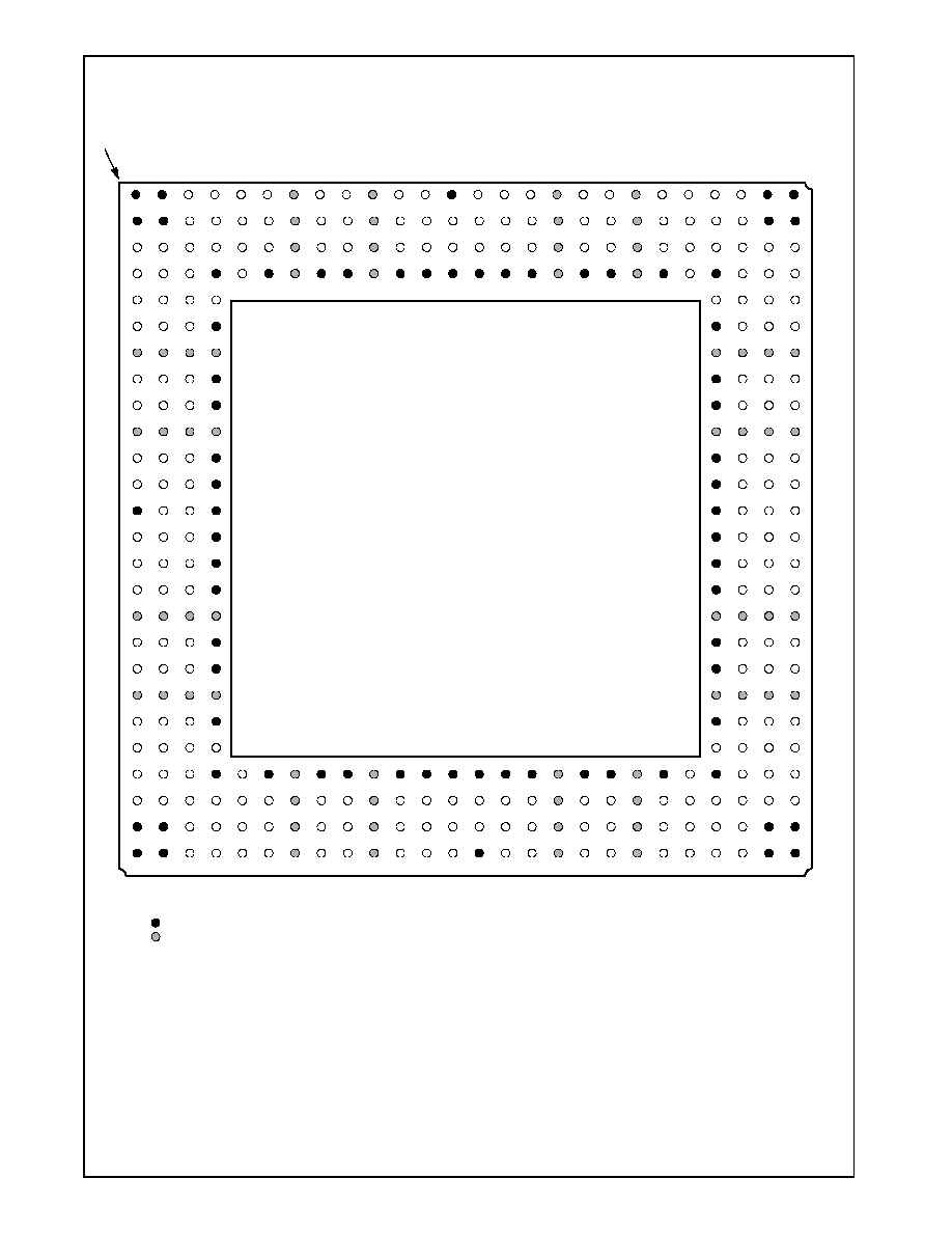
Figure 2-2 on page 14 shows the pin assignment for the
352 BGA with Tables 2-2 and 2-3 listing the pin assign-
ments sorted by pin number and alphabetically by signal
name, respectively.
Figure 2-3 on page 19 shows the pin assignment for the
320 SPGA with Tables 2-4 and 2-5 listing the pin assign-
ments sorted by pin number and alphabetically by signal
name, respectively.
In Section 2.2 "Signal Descriptions" starting on Page 24 a
description of each signal is provided within its associated
functional group.
Following the signal descriptions, information regarding
subsystem signal connections and split power planes and
decoupling is provided.
.
Figure 2-1. Functional Block Diagram
Table 2-1. Pin Type Definitions
Mnemonic
Definition
I
Standard input pin.
I/O
Bidirectional pin.
O
Totem-pole output.
OD
Open-drain output structure that allows
multiple devices to share the pin in a
wired-OR configuration
PU
Pull-up resistor
PD
Pull-down resistor
s/t/s
Sustained tri-state, an active-low tri-state
signal owned and driven by one and only
one agent at a time. The agent that
drives an s/t/s pin low must drive it high
for at least one clock before letting it float.
A new agent cannot start driving an s/t/s
signal any sooner than one clock after
the previous owner lets it float. A pull-up
resistor is required to sustain the inactive
state until another agent drives it, and
must be provided by the central resource.
VCC (PWR)
Power pin.
VSS (GND)
Ground pin
#
The "#" symbol at the end of a signal
name indicates that the active, or
asserted state occurs when the signal is
at a low voltage level. When "#" is not
present after the signal name, the signal
is asserted when at a high voltage level.
SYSCLK
CLKMODE[2:0]
RESET
INTR
IRQ13
SMI#
SUSP#
SUSPA#
SERIALP
AD[31:0]
C/BE[3:0]#
PAR
FRAME#
IRDY#
TRDY#
STOP#
LOCK#
DEVSEL#
PERR#
SERR#
REQ[2:0]#
GNT[2:0]#
MD[63:0]
MA[12:0]
BA[1:0]
RASA#, RASB#
CASA#, CASB#
CS[3:0]#
WEA#, WEB#
DQM[7:0]
CKEA, CKEB
SDCLK[3:0]
SDCLK_IN
SDCLK_OUT
PCLK
VID_CLK
DCLK
CRT_HSYNC
CRT_VSYNC
FP_VSYNC
FP_HSYNC
ENA_DISP
VID_RDY
VID_VAL
VID_DATA[7:0]
PIXEL[17:0]
Memory
Controller
Interface
Video
Interface
Signals
PCI
Interface
Signals
System
Interface
Signals
Signals
GeodeTM GXm
Processor
www.national.com
14
Revision 3.1
Signal Definitions (
Continued
)
GeodeTM
G
Xm
Pr
ocessor
Figure 2-2. 352 BGA Pin Assignment Diagram
For order information refer to Section A.1 "Order Information" on page 236.
1
2
3
4
5
6
7
8
9
10
11
12
13
14
15
16
17
18
19
20
21
22
23
24
25
26
A
B
C
D
E
F
G
H
J
K
L
M
N
P
R
T
U
V
W
Y
AA
AB
AC
AD
AE
AF
Index Corner
VSS
VSS
AD27 AD24 AD21 AD16 VCC2 FRAM#DEVS# VCC3 PERR# AD15
VSS
AD11 CBE0# AD6
VCC2
AD4
AD2
VCC3
AD0
AD1 TEST2 MD2
VSS
VSS
VSS
VSS
AD28 AD25 AD22 AD18 VCC2 CBE2# TRDY# VCC3 LOCK# PAR
AD14 AD12
AD9
AD7
VCC2 INTR
AD3
VCC3 TEST1 TEST3 MD1
MD33
VSS
VSS
AD29 AD31 AD30 AD26 AD23 AD19 VCC2 AD17 IRDY# VCC3 STOP# SERR# CBE1# AD13
AD10
AD8
VCC2
AD5
SMI# VCC3 TEST0 IRQ13 MD32 MD34
MD3
MD35
GNT0#
TDI
REQ2# VSS CBE3# VSS
VCC2
VSS
VSS
VCC3
VSS
VSS
VSS
VSS
VSS
VSS VCC2
VSS
VSS VCC3
VSS
MD0
VSS
MD4
MD36
TDN
GNT2#SUSPA#REQ0# AD20
MD6
TDP
MD5
MD37
TD0 GNT1# TEST
VSS
VSS
MD38
MD7
MD39
VCC3 VCC3 VCC3 VCC3
VCC3 VCC3 VCC3 VCC3
TMS SUSP# REQ1# VSS
VSS
MD8
MD40
MD9
FPVSY TCLK RESET VSS
VSS
MD41 MD10 MD42
VCC2 VCC2 VCC2 VCC2
VCC2 VCC2 VCC2 VCC2
CKM1 FPHSYSERLP VSS
VSS
MD11 MD43 MD12
CKM2 VIDVAL CKM0
VSS
VSS
MD44 MD13 MD45
VSS
PIX1
PIX0
VSS
VSS
MD14 MD46 MD15
VIDCLK PIX3
PIX2
VSS
VSS
MD47 CASA#SYSCLK
PIX4
PIX5
PIX6
VSS
VSS
WEB# WEA# CASB#
PIX7
PIX8
PIX9
VSS
VSS
DQM0 DQM4 DQM1
VCC3 VCC3 VCC3 VCC3
VCC3 VCC3 VCC3 VCC3
PIX10 PIX11 PIX12
VSS
VSS
DQM5 CS2# CS0#
PIX13 CRTHS PIX14
VSS
VSS RASA# RASB# MA0
VCC2 VCC2 VCC2 VCC2
VCC2 VCC2 VCC2 VCC2
PIX15 PIX16 CRTVS VSS
VSS
MA1
MA2
MA3
DCLK PIX17 VDAT6 VDAT7
MA4
MA5
MA6
MA7
PCLK
FLT# VDAT4 VSS VOLDET VSS
VCC2
VSS
VSS
VCC3
VSS
VSS
VSS
VSS
VSS
VSS
VCC2
VSS
VSS
VCC3
VSS
DQM6
VSS
MA8
MA9
MA10
VRDY VDAT5 VDAT3 VDAT0 EDISP MD63 VCC2 MD62 MD29 VCC3 MD59 MD26 MD56 MD55 MD22 CKEB VCC2 MD51 MD18 VCC3 MD48 DQM3 CS1# MA11
BA0
BA1
VSS
VSS VDAT2 SCLK3 SCLK1RWCLK VCC2 SCKIN MD61 VCC3 MD28 MD58 MD25 MD24 MD54 MD21 VCC2 MD20 MD50 VCC3 MD17 DQM7 CS3# MA12
VSS
VSS
VSS
VSS VDAT1 SCLK0 SCLK2 MD31 VCC2SCKOUTMD30 VCC3 MD60 MD27 MD57
VSS
MD23 MD53 VCC2 MD52 MD19 VCC3 MD49 MD16 DQM2 CKEA
VSS
VSS
1
2
3
4
5
6
7
8
9
10
11
12
13
14
15
16
17
18
19
20
21
22
23
24
25
26
A
B
C
D
E
F
G
H
J
K
L
M
N
P
R
T
U
V
W
Y
AA
AB
AC
AD
AE
AF
GeodeTM GXm
352 BGA - Top View
Note: Signal names have been abbreviated in this figure due to space constraints.
= GND terminal
= PWR terminal (VCC2 = VCC_CORE; VCC3 = VCC_IO)
Processor
Revision 3.1
15
www.national.com
Signal Definitions (
Continued
)
GeodeTM
G
Xm
P
r
ocessor
Table 2-2. 352 BGA Pin Assignments - Sorted by Pin Number
Pin
No.
Signal Name
A1 VSS
A2 VSS
A3 AD27
A4 AD24
A5 AD21
A6 AD16
A7 VCC2
A8 FRAME#
A9 DEVSEL#
A10 VCC3
A11 PERR#
A12 AD15
A13 VSS
A14 AD11
A15 C/BE0#
A16 AD6
A17 VCC2
A18 AD4
A19 AD2
A20 VCC3
A21 AD0
A22 AD1
A23 TEST2
A24 MD2
A25 VSS
A26 VSS
B1 VSS
B2 VSS
B3 AD28
B4 AD25
B5 AD22
B6 AD18
B7 VCC2
B8 C/BE2#
B9 TRDY#
B10 VCC3
B11 LOCK#
B12 PAR
B13 AD14
B14 AD12
B15 AD9
B16 AD7
B17 VCC2
B18 INTR
B19 AD3
B20 VCC3
B21 TEST1
B22 TEST3
B23 MD1
B24 MD33
B25 VSS
B26 VSS
C1 AD29
C2 AD31
C3 AD30
C4 AD26
C5 AD23
C6 AD19
C7 VCC2
C8 AD17
C9 IRDY#
C10 VCC3
C11 STOP#
C12 SERR#
C13 C/BE1#
C14 AD13
C15 AD10
C16 AD8
C17 VCC2
C18 AD5
C19 SMI#
C20 VCC3
C21 TEST0
C22 IRQ13
C23 MD32
C24 MD34
C25 MD3
C26 MD35
D1 GNT0#
D2 TDI
D3 REQ2#
D4 VSS
D5 C/BE3#
D6 VSS
D7 VCC2
D8 VSS
D9 VSS
D10 VCC3
D11 VSS
D12 VSS
D13 VSS
D14 VSS
D15 VSS
D16 VSS
D17 VCC2
D18 VSS
Pin
No.
Signal Name
D19 VSS
D20 VCC3
D21 VSS
D22 MD0
D23 VSS
D24 MD4
D25 MD36
D26 TDN
E1 GNT2#
E2 SUSPA#
E3 REQ0#
E4 AD20
E23 MD6
E24 TDP
E25 MD5
E26 MD37
F1 TDO
F2 GNT1#
F3 TEST
F4 VSS
F23 VSS
F24 MD38
F25 MD7
F26 MD39
G1 VCC3
G2 VCC3
G3 VCC3
G4 VCC3
G23 VCC3
G24 VCC3
G25 VCC3
G26 VCC3
H1 TMS
H2 SUSP#
H3 REQ1#
H4 VSS
H23 VSS
H24 MD8
H25 MD40
H26 MD9
J1 FP_VSYNC
J2 TCLK
J3 RESET
J4 VSS
J23 VSS
J24 MD41
J25 MD10
J26 MD42
Pin
No.
Signal Name
K1 VCC2
K2 VCC2
K3 VCC2
K4 VCC2
K23 VCC2
K24 VCC2
K25 VCC2
K26 VCC2
L1 CLKMODE1
L2 FP_HSYNC
L3 SERIALP
L4 VSS
L23 VSS
L24 MD11
L25 MD43
L26 MD12
M1 CLKMODE2
M2 VID_VAL
M3 CLKMODE0
M4 VSS
M23 VSS
M24 MD44
M25 MD13
M26 MD45
N1 VSS
N2 PIXEL1
N3 PIXEL0
N4 VSS
N23 VSS
N24 MD14
N25 MD46
N26 MD15
P1 VID_CLK
P2 PIXEL3
P3 PIXEL2
P4 VSS
P23 VSS
P24 MD47
P25 CASA#
P26 SYSCLK
R1 PIXEL4
R2 PIXEL5
R3 PIXEL6
R4 VSS
R23 VSS
R24 WEB#
R25 WEA#
R26 CASB#
Pin
No.
Signal Name
T1 PIXEL7
T2 PIXEL8
T3 PIXEL9
T4 VSS
T23 VSS
T24 DQM0
T25 DQM4
T26 DQM1
U1 VCC3
U2 VCC3
U3 VCC3
U4 VCC3
U23 VCC3
U24 VCC3
U25 VCC3
U26 VCC3
V1 PIXEL10
V2 PIXEL11
V3 PIXEL12
V4 VSS
V23 VSS
V24 DQM5
V25 CS2#
V26 CS0#
W1 PIXEL13
W2 CRT_HSYNC
W3 PIXEL14
W4 VSS
W23 VSS
W24 RASA#
W25 RASB#
W26 MA0
Y1 VCC2
Y2 VCC2
Y3 VCC2
Y4 VCC2
Y23 VCC2
Y24 VCC2
Y25 VCC2
Y26 VCC2
AA1 PIXEL15
AA2 PIXEL16
AA3 CRT_VSYNC
AA4 VSS
AA23 VSS
AA24 MA1
AA25 MA2
AA26 MA3
Pin
No.
Signal Name

www.national.com
16
Revision 3.1
Signal Definitions (
Continued
)
GeodeTM
G
Xm
Pr
ocessor
AB1 DCLK
AB2 PIXEL17
AB3 VID_DATA6
AB4 VID_DATA7
AB23 MA4
AB24 MA5
AB25 MA6
AB26 MA7
AC1 PCLK
AC2 FLT#
AC3 VID_DATA4
AC4 VSS
AC5 VOLDET
AC6 VSS
AC7 VCC2
AC8 VSS
AC9 VSS
AC10 VCC3
AC11 VSS
AC12 VSS
AC13 VSS
AC14 VSS
AC15 VSS
Pin
No.
Signal Name
AC16 VSS
AC17 VCC2
AC18 VSS
AC19 VSS
AC20 VCC3
AC21 VSS
AC22 DQM6
AC23 VSS
AC24 MA8
AC25 MA9
AC26 MA10
AD1 VID_RDY
AD2 VID_DATA5
AD3 VID_DATA3
AD4 VID_DATA0
AD5 ENA_DISP
AD6 MD63
AD7 VCC2
AD8 MD62
AD9 MD29
AD10 VCC3
AD11 MD59
AD12 MD26
Pin
No.
Signal Name
AD13 MD56
AD14 MD55
AD15 MD22
AD16 CKEB
AD17 VCC2
AD18 MD51
AD19 MD18
AD20 VCC3
AD21 MD48
AD22 DQM3
AD23 CS1#
AD24 MA11
AD25 BA0
AD26 BA1
AE1 VSS
AE2 VSS
AE3 VID_DATA2
AE4 SDCLK3
AE5 SDCLK1
AE6 RW_CLK
AE7 VCC2
AE8 SDCLK_IN
AE9 MD61
Pin
No.
Signal Name
AE10 VCC3
AE11 MD28
AE12 MD58
AE13 MD25
AE14 MD24
AE15 MD54
AE16 MD21
AE17 VCC2
AE18 MD20
AE19 MD50
AE20 VCC3
AE21 MD17
AE22 DQM7
AE23 CS3#
AE24 MA12
AE25 VSS
AE26 VSS
AF1 VSS
AF2 VSS
AF3 VID_DATA1
AF4 SDCLK0
AF5 SDCLK2
AF6 MD31
Pin
No.
Signal Name
AF7 VCC2
AF8 SDCLK_OUT
AF9 MD30
AF10 VCC3
AF11 MD60
AF12 MD27
AF13 MD57
AF14 VSS
AF15 MD23
AF16 MD53
AF17 VCC2
AF18 MD52
AF19 MD19
AF20 VCC3
AF21 MD49
AF22 MD16
AF23 DQM2
AF24 CKEA
AF25 VSS
AF26 VSS
Pin
No.
Signal Name
Table 2-2.
352 BGA Pin Assignments - Sorted by Pin Number (Continued)
Revision 3.1
17
www.national.com
Signal Definitions (
Continued
)
GeodeTM
G
Xm
P
r
ocessor
Table 2-3. 352 BGA Pin Assignments - Sorted Alphabetically by Signal Name
Signal Name
Type
Pin No.
AD0
I/O
A21
AD1
I/O
A22
AD2
I/O
A19
AD3
I/O
B19
AD4
I/O
A18
AD5
I/O
C18
AD6
I/O
A16
AD7
I/O
B16
AD8
I/O
C16
AD9
I/O
B15
AD10
I/O
C15
AD11
I/O
A14
AD12
I/O
B14
AD13
I/O
C14
AD14
I/O
B13
AD15
I/O
A12
AD16
I/O
A6
AD17
I/O
C8
AD18
I/O
B6
AD19
I/O
C6
AD20
I/O
E4
AD21
I/O
A5
AD22
I/O
B5
AD23
I/O
C5
AD24
I/O
A4
AD25
I/O
B4
AD26
I/O
C4
AD27
I/O
A3
AD28
I/O
B3
AD29
I/O
C1
AD30
I/O
C3
AD31
I/O
C2
BA0
O
AD25
BA1
O
AD26
CASA#
O
P25
CASB#
O
R26
C/BE0#
I/O
A15
C/BE1#
I/O
C13
C/BE2#
I/O
B8
C/BE3#
I/O
D5
CKEA
O
AF24
CKEB
O
AD16
CLKMODE0
I
M3
CLKMODE1
I
L1
CLKMODE2
I
M1
CRT_HSYNC
O
W2
CRT_VSYNC
O
AA3
CS0#
O
V26
CS1#
O
AD23
CS2#
O
V25
CS3#
O
AE23
DCLK
I
AB1
DEVSEL#
s/t/s
A9 (PU)
DQM0
O
T24
DQM1
O
T26
DQM2
O
AF23
DQM3
O
AD22
DQM4
O
T25
DQM5
O
V24
DQM6
O
AC22
DQM7
O
AE22
ENA_DISP
O
AD5
FLT#
I
AC2
FP_HSYNC
O
L2
FP_VSYNC
O
J1
FRAME#
s/t/s
A8 (PU)
GNT0#
O
D1
GNT1#
O
F2
GNT2#
O
E1
INTR
I
B18
IRDY#
s/t/s
C9 (PU)
IRQ13
O
C22
LOCK#
s/t/s
B11 (PU)
MA0
O
W26
MA1
O
AA24
MA2
O
AA25
MA3
O
AA26
MA4
O
AB23
MA5
O
AB24
MA6
O
AB25
MA7
O
AB26
MA8
O
AC24
MA9
O
AC25
MA10
O
AC26
MA11
O
AD24
MA12
O
AE24
MD0
I/O
D22
MD1
I/O
B23
MD2
I/O
A24
MD3
I/O
C25
MD4
I/O
D24
MD5
I/O
E25
MD6
I/O
E23
MD7
I/O
F25
MD8
I/O
H24
MD9
I/O
H26
MD10
I/O
J25
MD11
I/O
L24
MD12
I/O
L26
MD13
I/O
M25
MD14
I/O
N24
MD15
I/O
N26
MD16
I/O
AF22
MD17
I/O
AE21
MD18
I/O
AD19
MD19
I/O
AF19
Signal Name
Type
Pin No.
MD20
I/O
AE18
MD21
I/O
AE16
MD22
I/O
AD15
MD23
I/O
AF15
MD24
I/O
AE14
MD25
I/O
AE13
MD26
I/O
AD12
MD27
I/O
AF12
MD28
I/O
AE11
MD29
I/O
AD9
MD30
I/O
AF9
MD31
I/O
AF6
MD32
I/O
C23
MD33
I/O
B24
MD34
I/O
C24
MD35
I/O
C26
MD36
I/O
D25
MD37
I/O
E26
MD38
I/O
F24
MD39
I/O
F26
MD40
I/O
H25
MD41
I/O
J24
MD42
I/O
J26
MD43
I/O
L25
MD44
I/O
M24
MD45
I/O
M26
MD46
I/O
N25
MD47
I/O
P24
MD48
I/O
AD21
MD49
I/O
AF21
MD50
I/O
AE19
MD51
I/O
AD18
MD52
I/O
AF18
MD53
I/O
AF16
MD54
I/O
AE15
MD55
I/O
AD14
MD56
I/O
AD13
MD57
I/O
AF13
MD58
I/O
AE12
MD59
I/O
AD11
MD60
I/O
AF11
MD61
I/O
AE9
MD62
I/O
AD8
MD63
I/O
AD6
PAR
I/O
B12
PCLK
O
AC1
PERR#
s/t/s
A11 (PU)
PIXEL0
O
N3
PIXEL1
O
N2
PIXEL2
O
P3
PIXEL3
O
P2
PIXEL4
O
R1
PIXEL5
O
R2
Signal Name
Type
Pin No.
PIXEL6
O
R3
PIXEL7
O
T1
PIXEL8
O
T2
PIXEL9
O
T3
PIXEL10
O
V1
PIXEL11
O
V2
PIXEL12
O
V3
PIXEL13
O
W1
PIXEL14
O
W3
PIXEL15
O
AA1
PIXEL16
O
AA2
PIXEL17
O
AB2
RASA#
O
W24
RASB#
O
W25
REQ0#
I
E3 (PU)
REQ1#
I
H3 (PU)
REQ2#
I
D3 (PU)
RESET
I
J3
RW_CLK
O
AE6
SDCLK_IN
I
AE8
SDCLK_OUT
O
AF8
SDCLK0
O
AF4
SDCLK1
O
AE5
SDCLK2
O
AF5
SDCLK3
O
AE4
SERIALP
O
L3
SERR#
OD
C12 (PU)
SMI#
I
C19
STOP#
s/t/s
C11 (PU)
SUSP#
I
H2 (PU)
SUSPA#
O
E2
SYSCLK
I
P26
TCLK
I
J2 (PU)
TDI
I
D2 (PU)
TDN
O
D26
TDO
O
F1
TDP
O
E24
TEST
I
F3 (PD)
TEST0
O
C21
TEST1
O
B21
TEST2
O
A23
TEST3
O
B22
TMS
I
H1 (PU)
TRDY#
s/t/s
B9 (PU)
VCC2
PWR
A7
VCC2
PWR
A17
VCC2
PWR
B7
VCC2
PWR
B17
VCC2
PWR
C7
VCC2
PWR
C17
VCC2
PWR
D7
VCC2
PWR
D17
VCC2
PWR
K1
Signal Name
Type
Pin No.
www.national.com
18
Revision 3.1
Signal Definitions (
Continued
)
GeodeTM
G
Xm
Pr
ocessor
Note: PU/PD indicates pin is
internally connected to
a 20-kohm pull-up/-
down resistor.
VCC2
PWR
K2
VCC2
PWR
K3
VCC2
PWR
K4
VCC2
PWR
K23
VCC2
PWR
K24
VCC2
PWR
K25
VCC2
PWR
K26
VCC2
PWR
Y1
VCC2
PWR
Y2
VCC2
PWR
Y3
VCC2
PWR
Y4
VCC2
PWR
Y23
VCC2
PWR
Y24
VCC2
PWR
Y25
VCC2
PWR
Y26
VCC2
PWR
AC7
VCC2
PWR
AC17
VCC2
PWR
AD7
VCC2
PWR
AD17
VCC2
PWR
AE7
VCC2
PWR
AE17
VCC2
PWR
AF7
VCC2
PWR
AF17
VCC3
PWR
A10
VCC3
PWR
A20
VCC3
PWR
B10
VCC3
PWR
B20
VCC3
PWR
C10
VCC3
PWR
C20
VCC3
PWR
D10
VCC3
PWR
D20
VCC3
PWR
G1
VCC3
PWR
G2
VCC3
PWR
G3
VCC3
PWR
G4
VCC3
PWR
G23
VCC3
PWR
G24
Signal Name
Type
Pin No.
VCC3
PWR
G25
VCC3
PWR
G26
VCC3
PWR
U1
VCC3
PWR
U2
VCC3
PWR
U3
VCC3
PWR
U4
VCC3
PWR
U23
VCC3
PWR
U24
VCC3
PWR
U25
VCC3
PWR
U26
VCC3
PWR
AC10
VCC3
PWR
AC20
VCC3
PWR
AD10
VCC3
PWR
AD20
VCC3
PWR
AE10
VCC3
PWR
AE20
VCC3
PWR
AF10
VCC3
PWR
AF20
VID_CLK
O
P1
VID_DATA0
O
AD4
VID_DATA1
O
AF3
VID_DATA2
O
AE3
VID_DATA3
O
AD3
VID_DATA4
O
AC3
VID_DATA5
O
AD2
VID_DATA6
O
AB3
VID_DATA7
O
AB4
VID_RDY
I
AD1
VID_VAL
O
M2
VOLDET
O
AC5
VSS
GND
A1
VSS
GND
A2
VSS
GND
A13
VSS
GND
A25
VSS
GND
A26
VSS
GND
B1
VSS
GND
B2
Signal Name
Type
Pin No.
VSS
GND
B25
VSS
GND
B26
VSS
GND
D4
VSS
GND
D6
VSS
GND
D8
VSS
GND
D9
VSS
GND
D11
VSS
GND
D12
VSS
GND
D13
VSS
GND
D14
VSS
GND
D15
VSS
GND
D16
VSS
GND
D18
VSS
GND
D19
VSS
GND
D21
VSS
GND
D23
VSS
GND
F4
VSS
GND
F23
VSS
GND
H4
VSS
GND
H23
VSS
GND
J4
VSS
GND
J23
VSS
GND
L4
VSS
GND
L23
VSS
GND
M4
VSS
GND
M23
VSS
GND
N1
VSS
GND
N4
VSS
GND
N23
VSS
GND
P4
VSS
GND
P23
VSS
GND
R4
VSS
GND
R23
VSS
GND
T4
VSS
GND
T23
VSS
GND
V4
VSS
GND
V23
Signal Name
Type
Pin No.
VSS
GND
W4
VSS
GND
W23
VSS
GND
AA4
VSS
GND
AA23
VSS
GND
AC4
VSS
GND
AC6
VSS
GND
AC8
VSS
GND
AC9
VSS
GND
AC11
VSS
GND
AC12
VSS
GND
AC13
VSS
GND
AC14
VSS
GND
AC15
VSS
GND
AC16
VSS
GND
AC18
VSS
GND
AC19
VSS
GND
AC21
VSS
GND
AC23
VSS
GND
AE1
VSS
GND
AE2
VSS
GND
AE25
VSS
GND
AE26
VSS
GND
AF1
VSS
GND
AF2
VSS
GND
AF14
VSS
GND
AF25
VSS
GND
AF26
WEA#
O
R25
WEB#
O
R24
Signal Name
Type
Pin No.
Table 2-3.
352 BGA Pin Assignments - Sorted Alphabetically by Signal Name (Continued)
Revision 3.1
19
www.national.com
Signal Definitions (
Continued
)
GeodeTM
G
Xm
P
r
ocessor
Figure 2-3. 320 SPGA Pin Assignment Diagram
For order information refer to Section A.1 "Order Information" on page 236.
1
2
3
4
5
6
7
8
9
10 11 12 13 14 15 16 17 18 19 20 21 22 23 24 25 26
A
B
C
D
E
F
G
H
J
K
L
M
N
P
Q
R
S
T
U
V
AA
AB
AC
AD
AE
AF
Index Corner
27 28 29 30 31 32 33 34 35 36 37
AG
AH
AJ
AK
AL
AM
W
Y
X
Z
AN
A
B
C
D
E
F
G
H
J
K
L
M
N
P
Q
R
S
T
U
V
AA
AB
AC
AD
AE
AF
AG
AH
AJ
AK
AL
AM
W
Y
X
Z
AN
1
2
3
4
5
6
7
8
9
10 11 12 13 14 15 16 17 18 19 20 21 22 23 24 25 26 27 28 29 30 31 32 33 34 35 36 37
VCC3
AD25
VSS
VCC2
AD16
VCC3
STOP#
SERR#
VSS
AD11
AD8
VCC3
AD2
VCC2
VSS
TST0
VCC3
VSS
VSS
AD27
CBE3#
AD21
AD19
CBE2#
TRDY#
LOCK#
CBE1#
AD13
AD9
AD6
AD3
SMI#
AD1
TST2
MD33
MD2
VCC3
AD31
AD26
AD23
VCC2
AD18
FRAME#
VSS
PAR
VCC3
AD10
VSS
AD4
AD0
VCC2
IRQ13
MD1
MD34
VCC3
AD30
AD29
AD24
AD22
AD20
AD17
IRDY#
PERR#
AD14
AD12
AD7
INTR
TST1
TST3
MD0
MD32
MD3
MD35
REQ0#
REQ2#
AD28
VSS
VCC2
VCC2
VSS
DEVSEL#
AD15
VSS
CBE0#
AD5
VSS
VCC2
VCC2
VSS
MD4
MD36
TDN
GNT0#
TDI
MD5
TDP
VSS
CLKMODE2
VSS
VSS
MD37
VSS
GNT2#
SUSPA#
TDO
VSS
TEST
REQ1#
GNT1#
VCC2
VCC2
VCC2
RESET
SUSP#
VCC3
TMS
VSS
FPVSYN
TCK
SERIALP
VSS
NC
CKMD1 FPHSYN
CKMD0
VID_VAL
PIX0
PIX1
PIX2
VSS
VCC3
VSS
PIX3
VID_CLK
PIX6
PIX5
PIX4
NC
PIX9
PIX8
VSS
PIX7
NC
PIX10
VCC3
PIX11
VSS
PIX12
PIX13
VCC2
VCC2
VCC2
CRTHSYN
DCLK
PIX14
VSS
VCC2
PIX15
PIX16
VSS
PIX17
VSS
CRTVSYN VDAT6
MD6
MD38
VCC2
VSS
MD7
MD39
MD8
VCC2
VCC2
VCC2
MD40
MD9
VSS
MD41
VCC3
MD10
MD42
MD11
VSS
MD43
MD44
MD12
MD14
MD13
MD45
MD15
MD46
VSS
VCC3
VSS
SYSCLK
MD47
WEA#
WEB#
CASA#
DQM0
CASB#
DQM1
VSS
DQM4
CS2#
DQM5
VSS
CS0#
VCC3
RASB#
RASA#
VCC2
VCC2
VCC2
VCC2
VSS
MA1
MA2
MA0
MA4
MA3
VSS
MA5
VSS
MA8
MA6
MA10
PCLK
FLT#
VDAT5
VSS
VCC2
MD31
VSS
MD60
MD57
VSS
MD22
MD52
VSS
VCC2
VCC2
VSS
BA1
MA9
MA7
VRDY
VSS
VDAT0
SDCLK0 SDCLK2 SDCLKIN
MD29
MD27
MD56
MD55
MD21
MD20
MD50
MD16
DQM3
CS3#
VSS
BA0
VCC2
VDAT4
VDAT2
SDCLK1
VCC2
RWCLK SDCLKOUT
VSS
MD58
VCC3
MD23
VSS
MD19
MD49
VCC2
DQM6
CKEA
MA11
VCC3
VDAT7
VDAT3
ENDIS
SDCLK3
MD63
MD30
MD61
MD59
MD25
MD24
MD53
MD51
MD18
MD48
DQM7
DQM2
MA12
VOLDET
VSS
VCC2
VDAT1
VSS
VCC2
MD62
VCC3
MD28
MD26
VSS
MD54
CKEB
VCC3
MD17
VCC2
VSS
CS1#
VCC3
VSS
Note: Signal names have been abbreviated in this figure due to space constraints.
= Denotes GND terminal
= Denotes PWR terminal (VCC2 = VCC_CORE; VCC3 = VCC_IO)
320 SPGA - Top View
Processor
GeodeTM GXm
www.national.com
20
Revision 3.1
Signal Definitions (
Continued
)
GeodeTM
G
Xm
Pr
ocessor
Table 2-4. 320 SPGA Pin Assignments - Sorted by Pin Number
Pin
No.
Signal Name
A3 VCC3
A5 AD25
A7 VSS
A9 VCC2
A11 AD16
A13 VCC3
A15 STOP#
A17 SERR#
A19 VSS
A21 AD11
A23 AD8
A25 VCC3
A27 AD2
A29 VCC2
A31 VSS
A33 TEST0
A35 VCC3
A37 VSS
B2 VSS
B4 AD27
B6 C/BE3#
B8 AD21
B10 AD19
B12 C/BE2#
B14 TRDY#
B16 LOCK#
B18 C/BE1#
B20 AD13
B22 AD9
B24 AD6
B26 AD3
B28 SMI#
B30 AD1
B32 TEST2
B34 MD33
B36 MD2
C1 VCC3
C3 AD31
C5 AD26
C7 AD23
C9 VCC2
C11 AD18
C13 FRAME#
C15 VSS
C17 PAR
C19 VCC3
C21 AD10
C23 VSS
C25 AD4
C27 AD0
C29 VCC2
C31 IRQ13
C33 MD1
C35 MD34
C37 VCC3
D2 AD30
D4 AD29
D6 AD24
D8 AD22
D10 AD20
D12 AD17
D14 IRDY#
D16 PERR#
D18 AD14
D20 AD12
D22 AD7
D24 INTR
D26 TEST1
D28 TEST3
D30 MD0
D32 MD32
D34 MD3
D36 MD35
E1 REQ0#
E3 REQ2#
E5 AD28
E7 VSS
E9 VCC2
E11 VCC2
E13 VSS
E15 DEVSEL#
E17 AD15
E19 VSS
E21 C/BE0#
E23 AD5
E25 VSS
E27 VCC2
E29 VCC2
E31 VSS
E33 MD4
E35 MD36
E37 TDN
F2 GNT0#
F4 TDI
F34 MD5
F36 TDP
Pin
No.
Signal Name
G1 VSS
G3 CLKMODE2
G5 VSS
G33 VSS
G35 MD37
G37 VSS
H2 GNT2#
H4 SUSPA#
H34 MD6
H36 MD38
J1 TDO
J3 VSS
J5 TEST
J33 VCC2
J35 VSS
J37 MD7
K2 REQ1#
K4 GNT1#
K34 MD39
K36 MD8
L1 VCC2
L3 VCC2
L5 VCC2
L33 VCC2
L35 VCC2
L37 VCC2
M2 RESET
M4 SUSP#
M34 MD40
M36 MD9
N1 VCC3
N3 TMS
N5 VSS
N33 VSS
N35 MD41
N37 VCC3
P2 FP_VSYNC
P4 TCLK
P34 MD10
P36 MD42
Q1 SERIALP
Q3 VSS
Q5 NC
Q33 MD11
Q35 VSS
Q37 MD43
R2 CLKMODE1
R4 FP_HSYNC
Pin
No.
Signal Name
R34 MD44
R36 MD12
S1 CLKMODE0
S3 VID_VAL
S5 PIXEL0
S33 MD14
S35 MD13
S37 MD45
T2 PIXEL1
T4 PIXEL2
T34 MD15
T36 MD46
U1 VSS
U3 VCC3
U5 VSS
U33 VSS
U35 VCC3
U37 VSS
V2 PIXEL3
V4 VID_CLK
V34 SYSCLK
V36 MD47
W1 PIXEL6
W3 PIXEL5
W5 PIXEL4
W33 WEA#
W35 WEB#
W37 CASA#
X2 NC
X4 PIXEL9
X34 DQM0
X36 CASB#
Y1 PIXEL8
Y3 VSS
Y5 PIXEL7
Y33 DQM1
Y35 VSS
Y37 DQM4
Z2 NC
Z4 PIXEL10
Z34 CS2#
Z36 DQM5
AA1 VCC3
AA3 PIXEL11
AA5 VSS
AA33 VSS
AA35 CS0#
AA37 VCC3
Pin
No.
Signal Name
AB2 PIXEL12
AB4 PIXEL13
AB34 RASB#
AB36 RASA#
AC1 VCC2
AC3 VCC2
AC5 VCC2
AC33 VCC2
AC35 VCC2
AC37 VCC2
AD2 CRT_HSYNC
AD4 DCLK
AD34 MA2
AD36 MA0
AE1 PIXEL14
AE3 VSS
AE5 VCC2
AE33 VCC2
AE35 VSS
AE37 MA1
AF2 PIXEL15
AF4 PIXEL16
AF34 MA4
AF36 MA3
AG1 VSS
AG3 PIXEL17
AG5 VSS
AG33 VSS
AG35 MA5
AG37 VSS
AH2 CRT_VSYNC
AH4 VID_DATA6
AH32 MA10
AH34 MA8
AH36 MA6
AJ1 PCLK
AJ3 FTL#
AJ5 VID_DATA5
AJ7 VSS
AJ9 VCC2
AJ11 MD31
AJ13 VSS
AJ15 MD60
AJ17 MD57
AJ19 VSS
AJ21 MD22
AJ23 MD52
AJ25 VSS
Pin
No.
Signal Name
Revision 3.1
21
www.national.com
Signal Definitions (
Continued
)
GeodeTM
G
Xm
P
r
ocessor
AJ27 VCC2
AJ29 VCC2
AJ31 VSS
AJ33 BA1
AJ35 MA9
AJ37 MA7
AK2 VID_RDY
AK4 VSS
AK6 VID_DATA0
AK8 SDCLK0
AK10 SDCLK2
AK12 SDCLK_IN
AK14 MD29
AK16 MD27
AK18 MD56
AK20 MD55
AK22 MD21
Pin
No.
Signal Name
AK24 MD20
AK26 MD50
AK28 MD16
AK30 DQM3
AK32 CS3#
AK34 VSS
AK36 BA0
AL1 VCC2
AL3 VID_DATA4
AL5 VID_DATA2
AL7 SDCLK1
AL9 VCC2
AL11 RW_CLK
AL13 SDCLK_OUT
AL15 VSS
AL17 MD58
AL19 VCC3
Pin
No.
Signal Name
AL21 MD23
AL23 VSS
AL25 MD19
AL27 MD49
AL29 VCC2
AL31 DQM6
AL33 CKEA
AL35 MA11
AL37 VCC3
AM2 VID_DATA7
AM4 VID_DATA3
AM6 ENA_DISP
AM8 SDCLK3
AM10 MD63
AM12 MD30
AM14 MD61
AM16 MD59
Pin
No.
Signal Name
AM18 MD25
AM20 MD24
AM22 MD53
AM24 MD51
AM26 MD18
AM28 MD48
AM30 DQM7
AM32 DQM2
AM34 MA12
AM36 VOLDET
AN1 VSS
AN3 VCC2
AN5 VID_DATA1
AN7 VSS
AN9 VCC2
AN11 MD62
AN13 VCC3
Pin
No.
Signal Name
AN15 MD28
AN17 MD26
AN19 VSS
AN21 MD54
AN23 CKEB
AN25 VCC3
AN27 MD17
AN29 VCC2
AN31 VSS
AN33 CS1#
AN35 VCC3
AN37 VSS
Pin
No.
Signal Name
Table 2-4.
320 SPGA Pin Assignments - Sorted by Pin Number (Continued)

www.national.com
22
Revision 3.1
Signal Definitions (
Continued
)
GeodeTM
G
Xm
Pr
ocessor
Table 2-5. 320 SPGA Pin Assignments - Sorted Alphabetically by Signal Name
Signal Name
Type
Pin. No.
AD0
I/O
C27
AD1
I/O
B30
AD2
I/O
A27
AD3
I/O
B26
AD4
I/O
C25
AD5
I/O
E23
AD6
I/O
B24
AD7
I/O
D22
AD8
I/O
A23
AD9
I/O
B22
AD10
I/O
C21
AD11
I/O
A21
AD12
I/O
D20
AD13
I/O
B20
AD14
I/O
D18
AD15
I/O
E17
AD16
I/O
A11
AD17
I/O
D12
AD18
I/O
C11
AD19
I/O
B10
AD20
I/O
D10
AD21
I/O
B8
AD22
I/O
D8
AD23
I/O
C7
AD24
I/O
D6
AD25
I/O
A5
AD26
I/O
C5
AD27
I/O
B4
AD28
I/O
E5
AD29
I/O
D4
AD30
I/O
D2
AD31
I/O
C3
BA0
O
AK36
BA1
O
AJ33
CASA#
O
W37
CASB#
O
X36
C/BE0#
I/O
E21
C/BE1#
I/O
B18
C/BE2#
I/O
B12
C/BE3#
I/O
B6
CKEA
O
AL33
CKEB
O
AN23
CLKMODE0
I
S1
CLKMODE1
I
R2
CLKMODE2
I
G3
CRT_HSYNC
O
AD2
CRT_VSYNC
O
AH2
CS0#
O
AA35
CS1#
O
AN33
CS2#
O
Z34
CS3#
O
AK32
DCLK
I
AD4
DEVSEL#
s/t/s
E15 (PU)
DQM0
O
X34
DQM1
O
Y33
DQM2
O
AM32
DQM3
O
AK30
DQM4
O
Y37
DQM5
O
Z36
DQM6
O
AL31
DQM7
O
AM30
ENA_DISP
O
AM6
FLT#
I
AJ3
FP_HSYNC
O
R4
FP_VSYNC
O
P2
FRAME#
s/t/s
C13 (PU)
GNT0#
O
F2
GNT1#
O
K4
GNT2#
O
H2
INTR
I
D24
IRDY#
s/t/s
D14 (PU)
IRQ13
O
C31
LOCK#
s/t/s
B16 (PU)
MA0
O
AD36
MA1
O
AE37
MA2
O
AD34
MA3
O
AF36
MA4
O
AF34
MA5
O
AG35
MA6
O
AH36
MA7
O
AJ37
MA8
O
AH34
MA9
O
AJ35
MA10
O
AH32
MA11
O
AL35
MA12
O
AM34
MD0
I/O
D30
MD1
I/O
C33
MD2
I/O
B36
MD3
I/O
D34
MD4
I/O
E33
MD5
I/O
F34
MD6
I/O
H34
MD7
I/O
J37
MD8
I/O
K36
MD9
I/O
M36
MD10
I/O
P34
MD11
I/O
Q33
MD12
I/O
R36
MD13
I/O
S35
MD14
I/O
S33
MD15
I/O
T34
MD16
I/O
AK28
MD17
I/O
AN27
MD18
I/O
AM26
MD19
I/O
AL25
Signal Name
Type
Pin. No.
MD20
I/O
AK24
MD21
I/O
AK22
MD22
I/O
AJ21
MD23
I/O
AL21
MD24
I/O
AM20
MD25
I/O
AM18
MD26
I/O
AN17
MD27
I/O
AK16
MD28
I/O
AN15
MD29
I/O
AK14
MD30
I/O
AM12
MD31
I/O
AJ11
MD32
I/O
D32
MD33
I/O
B34
MD34
I/O
C35
MD35
I/O
D36
MD36
I/O
E35
MD37
I/O
G35
MD38
I/O
H36
MD39
I/O
K34
MD40
I/O
M34
MD41
I/O
N35
MD42
I/O
P36
MD43
I/O
Q37
MD44
I/O
R34
MD45
I/O
S37
MD46
I/O
T36
MD47
I/O
V36
MD48
I/O
AM28
MD49
I/O
AL27
MD50
I/O
AK26
MD51
I/O
AM24
MD52
I/O
AJ23
MD53
I/O
AM22
MD54
I/O
AN21
MD55
I/O
AK20
MD56
I/O
AK18
MD57
I/O
AJ17
MD58
I/O
AL17
MD59
I/O
AM16
MD60
I/O
AJ15
MD61
I/O
AM14
MD62
I/O
AN11
MD63
I/O
AM10
NC
Q5
NC
X2
NC
Z2
PAR
I/O
C17
PCLK
O
AJ1
PERR#
s/t/s
D16 (PU)
PIXEL0
O
S5
PIXEL1
O
T2
PIXEL2
O
T4
Signal Name
Type
Pin. No.
PIXEL3
O
V2
PIXEL4
O
W5
PIXEL5
O
W3
PIXEL6
O
W1
PIXEL7
O
Y5
PIXEL8
O
Y1
PIXEL9
O
X4
PIXEL10
O
Z4
PIXEL11
O
AA3
PIXEL12
O
AB2
PIXEL13
O
AB4
PIXEL14
O
AE1
PIXEL15
O
AF2
PIXEL16
O
AF4
PIXEL17
O
AG3
RASA#
O
AB36
RASB#
O
AB34
REQ0#
I
E1 (PU)
REQ1#
I
K2 (PU)
REQ2#
I
E3 (PU)
RESET
I
M2
RW_CLK
O
AL11
SDCLK_IN
I
AK12
SDCLK_OUT
O
AL13
SDCLK0
O
AK8
SDCLK1
O
AL7
SDCLK2
O
AK10
SDCLK3
O
AM8
SERIALP
O
Q1
SERR#
OD
A17 (PU)
SMI#
I
B28
STOP#
s/t/s
A15 (PU)
SUSP#
I
M4 (PU)
SUSPA#
O
H4
SYSCLK
I
V34
TCLK
I
P4 (PU)
TDI
I
F4 (PU)
TDN
O
E37
TDO
O
J1
TDP
O
F36
TEST
I
J5 (PD)
TEST0
O
A33
TEST1
O
D26
TEST2
O
B32
TEST3
O
D28
TMS
I
N3 (PU)
TRDY#
s/t/s
B14 (PU)
VCC2
PWR
A9
VCC2
PWR
A29
VCC2
PWR
C9
VCC2
PWR
C29
VCC2
PWR
E9
VCC2
PWR
E11
Signal Name
Type
Pin. No.

Revision 3.1
23
www.national.com
Signal Definitions (
Continued
)
GeodeTM
G
Xm
P
r
ocessor
Note: PU/PD indicates pin is
internally connected to
a 20-kohm pull-up/
down resistor
VCC2
PWR
E27
VCC2
PWR
E29
VCC2
PWR
J33
VCC2
PWR
L1
VCC2
PWR
L3
VCC2
PWR
L5
VCC2
PWR
L33
VCC2
PWR
L35
VCC2
PWR
L37
VCC2
PWR
AC1
VCC2
PWR
AC3
VCC2
PWR
AC5
VCC2
PWR
AC33
VCC2
PWR
AC35
VCC2
PWR
AC37
VCC2
PWR
AE5
VCC2
PWR
AE33
VCC2
PWR
AJ9
VCC2
PWR
AJ27
VCC2
PWR
AJ29
VCC2
PWR
AL1
VCC2
PWR
AL9
VCC2
PWR
AL29
VCC2
PWR
AN3
VCC2
PWR
AN9
VCC2
PWR
AN29
VCC3
PWR
A3
VCC3
PWR
A13
VCC3
PWR
A25
Signal Name
Type
Pin. No.
VCC3
PWR
A35
VCC3
PWR
C1
VCC3
PWR
C19
VCC3
PWR
C37
VCC3
PWR
N1
VCC3
PWR
N37
VCC3
PWR
U3
VCC3
PWR
U35
VCC3
PWR
AA1
VCC3
PWR
AA37
VCC3
PWR
AL19
VCC3
PWR
AL37
VCC3
PWR
AN13
VCC3
PWR
AN25
VCC3
PWR
AN35
VID_CLK
O
V4
VID_DATA0
O
AK6
VID_DATA1
O
AN5
VID_DATA2
O
AL5
VID_DATA3
O
AM4
VID_DATA4
O
AL3
VID_DATA5
O
AJ5
VID_DATA6
O
AH4
VID_DATA7
O
AM2
VID_RDY
I
AK2
VID_VAL
O
S3
VOLDET
O
AM36
VSS
GND
A7
VSS
GND
A19
Signal Name
Type
Pin. No.
VSS
GND
A31
VSS
GND
A37
VSS
GND
B2
VSS
GND
C15
VSS
GND
C23
VSS
GND
E7
VSS
GND
E13
VSS
GND
E19
VSS
GND
E25
VSS
GND
E31
VSS
GND
G1
VSS
GND
G5
VSS
GND
G33
VSS
GND
G37
VSS
GND
J3
VSS
GND
J35
VSS
GND
N5
VSS
GND
N33
VSS
GND
Q3
VSS
GND
Q35
VSS
GND
U1
VSS
GND
U5
VSS
GND
U33
VSS
GND
U37
VSS
GND
Y3
VSS
GND
Y35
VSS
GND
AA5
VSS
GND
AA33
VSS
GND
AE3
Signal Name
Type
Pin. No.
VSS
GND
AE35
VSS
GND
AG1
VSS
GND
AG5
VSS
GND
AG33
VSS
GND
AG37
VSS
GND
AJ7
VSS
GND
AJ13
VSS
GND
AJ19
VSS
GND
AJ25
VSS
GND
AJ31
VSS
GND
AK4
VSS
GND
AK34
VSS
GND
AL15
VSS
GND
AL23
VSS
GND
AN1
VSS
GND
AN7
VSS
GND
AN19
VSS
GND
AN31
VSS
GND
AN37
WEA#
O
W33
WEB#
O
W35
Signal Name
Type
Pin. No.
Table 2-5.
320 SPGA Pin Assignments - Sorted Alphabetically by Signal Name (Continued)

www.national.com
24
Revision 3.1
Signal Definitions (
Continued
)
GeodeTM
G
Xm
Pr
ocessor
2.2
SIGNAL DESCRIPTIONS
2.2.1
System Interface Signals
Signal Name
BGA
Pin No.
SPGA
Pin No.
Type
Description
SYSCLK
P26
V34
I
System Clock
System Clock runs synchronously with the PCI bus. The internal
clock of the GXm processor is generated by an internal PLL
which multiplies the SYSCLK input and can run up to eight times
faster. The SYSCLK to core clock multiplier is configured using
the CLKMOD[2:0] inputs.
The SYSCLK input is a fixed frequency which can only be
stopped or varied when the GXm processor is in a full 3V Sus-
pend. (Section 6.4 "3-Volt Suspend Mode" on page 174 for
details regarding this mode.)
CLKMODE[2:0]
M1, L1,
M3
G3, R2,
S1
I
Clock Mode
These signals are used to set the core clock multiplier. The PCI
clock "SYSCLK" is multiplied by the value programmed by CLK-
MODE[2:0] to generate the GXm processor's core clock.
CLKMODE2 is valid only for GXm processor revision 4.0 and up.
The value read from DIR1 (Device ID Register 1, refer to
page 51) affects the definition of the CLKMODE pins.
If DIR1 = 30h-33h then CLKMODE[1:0]:
00 = SYSCLK multiplied by 4 (Test mode only)
01 = SYSCLK multiplied by 6
10 = SYSCLK multiplied by 7
11 = SYSCLK multiplied by 5
If DIR1 = 34h-4Fh then CLKMODE[1:0]:
00 = SYSCLK multiplied by 4 (Test mode only)
01 = SYSCLK multiplied by 6
10 = SYSCLK multiplied by 7
11 = SYSCLK multiplied by 8
If DIR1 > or = 50h then CLKMODE[2:0]:
000 = SYSCLK multiplied by 4 (Test mode only)
001 = SYSCLK multiplied by 10
010 = SYSCLK multiplied by 9
011 = SYSCLK multiplied by 5
100 = SYSCLK multiplied by 4
101 = SYSCLK multiplied by 6
110 = SYSCLK multiplied by 7
111 = SYSCLK multiplied by 8
RESET
J3
M2
I
Reset
RESET aborts all operations in progress and places the
GXm processor into a reset state. RESET forces the CPU and
peripheral functions to begin executing at a known state. All data
in the on-chip cache is invalidated.
RESET is an asynchronous input but must meet specified setup
and hold times to guarantee recognition at a particular clock
edge. This input is typically generated during the Power-On-
Reset sequence.
Note:
Warm Reset does not require an input on the GXm pro-
cessor since the function is virtualized using SMM.

Revision 3.1
25
www.national.com
Signal Definitions (
Continued
)
GeodeTM
G
Xm
P
r
ocessor
INTR
B18
D24
I
(Maskable) Interrupt Request
INTR is a level-sensitive input that causes the GXm processor to
Suspend execution of the current instruction stream and begin
execution of an interrupt service routine. The INTR input can be
masked through the Flags Register IF bit. (See Table 3-4 on
page 43 for bit definitions.)
IRQ13
C22
C31
O
Interrupt Request Level 13
IRQ13 is asserted if an on-chip floating point error occurs.
When a floating point error occurs, the GXm processor asserts
the IRQ13 pin. The floating point interrupt handler then performs
an OUT instruction to I/O address F0h or F1h. The GXm proces-
sor accepts either of these cycles and clears the IRQ13 pin.
Refer to Section 3.4.1 "I/O Address Space" on page 60 for fur-
ther information on IN/OUT instructions.
SMI#
C19
B28
I
System Management Interrupt
SMI# is a level-sensitive interrupt. SMI# puts the GXm processor
into System Management Mode (SMM).
SUSP#
H2
(PU)
M4
(PU)
I
Suspend Request
This signal is used to request that the GXm processor enter Sus-
pend mode. After recognition of an active SUSP# input, the pro-
cessor completes execution of the current instruction, any
pending decoded instructions and associated bus cycles.
SUSP# is ignored following RESET# and is enabled by setting
the SUSP bit in CCR2. (See Table 16 on page 44 for CCR2 bit
definitions.)
Since the GXm processor includes system logic functions as well
as the CPU core, there are special modes designed to support
the different power management states associated with APM,
ACPI, and portable designs. The part can be configured to stop
only the CPU core clocks, or all clocks. When all clocks are
stopped, the external clock can also be stopped. (See Section
6.0 "Power Management" on page 174 for more details regarding
power management states.)
This pin is internally connected to a 20-kohm pull-up resistor.
SUSP# is pulled up when not active.
SUSPA#
E2
H4
O
Suspend Acknowledge
Suspend Acknowledge indicates that the GXm processor has
entered low-power Suspend mode as a result of SUSP# asser-
tion or execution of a HALT instruction. SUSPA# is enabled by
setting the SUSP bit in CCR2. (See Table 16 on page 44 for
CCR2 bit definitions.)
The SYSCLK input may be stopped after SUSPA# has been
asserted to further reduce power consumption if the system is
configured for 3V Suspend mode. (Section 6.4 "3-Volt Suspend
Mode" on page 174 for details regarding this mode.)
SERIALP
L3
Q1
O
Serial Packet
Serial Packet is the single wire serial-transmission signal to the
CS5530 chip. The clock used for this interface is the PCI clock
(SYSCLK). This interface carries packets of miscellaneous infor-
mation to the chipset to be used by the VSA software handlers.
2.2.1
System Interface Signals (Continued)
Signal Name
BGA
Pin No.
SPGA
Pin No.
Type
Description

www.national.com
26
Revision 3.1
Signal Definitions (
Continued
)
GeodeTM
G
Xm
Pr
ocessor
2.2.2
PCI Interface Signals
Signal Name
BGA
Pin No.
SPGA
Pin No
Type
Description
AD[31:0]
Refer
to Table
2-3
Refer
to Table
2-5
I/O
Multiplexed Address and Data
Addresses and data are multiplexed on the same PCI pins. A bus
transaction consists of an address phase in the cycle in which
FRAME# is asserted followed by one or more data phases. Dur-
ing the address phase, AD[31:0] contain a physical 32-bit
address. For I/O, this is a byte address, for configuration and
memory it is a DWORD address. During data phases, AD[7:0]
contain the least significant byte (LSB) and AD[31:24] contain
the most significant byte (MSB). Write data is stable and valid
when IRDY# is asserted and read data is stable and valid when
TRDY# is asserted. Data is transferred during those SYSCLKS
where both IRDY# and TRDY# are asserted.
C/BE[3:0]#
D5,
B8,
C13,
A15
B6,
B12,
B18,
E21
I/O
Multiplexed Command and Byte Enables
Bus command and byte enables are multiplexed on the same
PCI pins. During the address phase of a transaction when
FRAME# is active, C/BE[3:0]# define the bus command. During
the data phase C/BE[3:0]# are used as byte enables. The byte
enables are valid for the entire data phase and determine which
byte lanes carry meaningful data. C/BE0# applies to byte 0
(LSB) and C/BE3# applies to byte 3 (MSB).
The command encoding and types are listed below.
0000 = Interrupt Acknowledge
0001 = Special Cycle
0010 = I/O Read
0011 = I/O Write
0100 = Reserved
0101 = Reserved
0110 = Memory Read
0111 = Memory Write
1000 = Reserved
1001 = Reserved
1010 = Configuration Read
1011 = Configuration Write
1100 = Memory Read Multiple
1101 = Dual Address Cycle (Reserved)
1110 = Memory Read Line
1111 = Memory Write and Invalidate
PAR
B12
C17
I/O
Parity
Parity generation is required by all PCI agents: the master drives
PAR for address and write-data phases, the target drives PAR for
read-data phases. Parity is even across AD[31:0] and
C/BE[3:0]#.
For address phases, PAR is stable and valid one SYSCLK after
the address phase. It has the same timing as AD[31:0] but
delayed by one SYSCLK.
For data phases, PAR is stable and valid one SYSCLK after
either IRDY# is asserted on a write transaction or after TRDY# is
asserted on a read transaction. Once PAR is valid, it remains
valid until one SYSCLK after the completion of the data phase.
(Also see PERR#.)

Revision 3.1
27
www.national.com
Signal Definitions (
Continued
)
GeodeTM
G
Xm
P
r
ocessor
FRAME#
A8
(PU)
C13
(PU)
s/t/s
Frame
Cycle Frame is driven by the current master to indicate the
beginning and duration of an access. FRAME# is asserted to
indicate a bus transaction is beginning. While FRAME# is
asserted, data transfers continue. When FRAME# is deasserted,
the transaction is in the final data phase.
This pin is internally connected to a 20-kohm pull-up resistor.
IRDY#
C9
(PU)
D14
(PU)
s/t/s
Initiator Ready
Initiator Ready is asserted to indicate that the bus master is able
to complete the current data phase of the transaction. IRDY# is
used in conjunction with TRDY#. A data phase is completed on
any SYSCLK in which both IRDY# and TRDY# are sampled
asserted. During a write, IRDY# indicates valid data is present
on AD[31:0]. During a read, it indicates the master is prepared to
accept data. Wait cycles are inserted until both IRDY# and
TRDY# are asserted together.
This pin is internally connected to a 20-kohm pull-up resistor.
TRDY#
B9
(PU)
B14
(PU)
s/t/s
Target Ready
TRDY# is asserted to indicate that the target agent is able to
complete the current data phase of the transaction. TRDY# is
used in conjunction with IRDY#. A data phase is complete on any
SYSCLK in which both TRDY# and IRDY# are sampled
asserted. During a read, TRDY# indicates that valid data is
present on AD[31:0]. During a write, it indicates the target is pre-
pared to accept data. Wait cycles are inserted until both IRDY#
and TRDY# are asserted together.
This pin is internally connected to a 20-kohm pull-up resistor.
STOP#
C11
(PU)
A15
(PU)
s/t/s
Target Stop
STOP# is asserted to indicate that the current target is request-
ing the master to stop the current transaction. This signal is used
with DEVSEL# to indicate retry, disconnect or target abort. If
STOP# is sampled active while a master, FRAME# will be deas-
serted and the cycle stopped within three SYSCLK cycles. As an
input, STOP# can be asserted in the following cases. 1) If a PCI
master tries to access memory that has been locked by another
master. This condition is detected if FRAME# and LOCK# are
asserted during an address phase. 2) STOP# will also be
asserted if the PCI write buffers are full or if a previously buffered
cycle has not completed. 3) Finally, STOP# can be asserted on
read cycles that cross cache line boundaries. This is conditional
based upon the programming of bit 1 in PCI Control Function 2
Register. (See Table 4-37 on page 156 for programming details.)
This pin is internally connected to a 20-kohm pull-up resistor.
2.2.2
PCI Interface Signals (Continued)
Signal Name
BGA
Pin No.
SPGA
Pin No
Type
Description

www.national.com
28
Revision 3.1
Signal Definitions (
Continued
)
GeodeTM
G
Xm
Pr
ocessor
LOCK#
B11
(PU)
B16
(PU)
s/t/s
Lock Operation
LOCK# indicates an atomic operation that may require multiple
transactions to complete. When LOCK# is asserted, nonexclu-
sive transactions may proceed to an address that is not currently
locked (at least 16 bytes must be locked). A grant to start a trans-
action on PCI does not guarantee control of LOCK#. Control of
LOCK# is obtained under it own protocol in conjunction with
GNT#. It is possible for different agents to use PCI while a single
master retains ownership of LOCK#. The arbiter can implement
a complete system lock. In this mode, if LOCK# is active, no
other master can gain access to the system until the LOCK# is
deasserted.
This pin is internally connected to a 20-kohm pull-up resistor.
DEVSEL#
A9
(PU)
E15
(PU)
s/t/s
Device Select
DEVSEL# indicates that the driving device has decoded its
address as the target of the current access. As an input,
DEVSEL# indicates whether any device on the bus has been
selected. DEVSEL# will also be driven by any agent that has the
ability to accept cycles on a subtractive decode basis. As a mas-
ter, if no DEVSEL# is detected within and up to the subtractive
decode clock, a master abort cycle will result expect for special
cycles which do not expect a DEVSEL# returned.
This pin is internally connected to a 20-kohm pull-up resistor.
PERR#
A11
(PU)
D16
(PU)
s/t/s
Parity Error
PERR# is used for reporting of data parity errors during all PCI
transactions except a Special Cycle. The PERR# line is driven
two SYSCLKs after the data in which the error was detected.
This is one SYSCLK after the PAR that is attached to the data.
The minimum duration of PERR# is one SYSCLK for each data
phase in which a data parity error is detected. PERR# must be
driven high for one SYSCLK before being in TRI-STATE mode. A
target asserts PERR# on write cycles if it has claimed the cycle
with DEVSEL#. The master asserts PERR# on read cycles.
This pin is internally connected to a 20-kohm pull-up resistor.
SERR#
C12
(PU)
A17
(PU)
OD
System Error
System Error may be asserted by any agent for reporting errors
other than PCI parity. The intent is to have the PCI central agent
assert NMI to the processor. When the Parity Enable bit is set in
the Memory Controller Configuration register, SERR# will be
asserted upon detecting a parity error on read operations from
DRAM.
REQ[2:0]#
D3,
H3,
E3
(PU)
E3,
K2,
E1
(PU)
I
Request Lines
Request indicates to the arbiter that an agent desires use of the
bus. Each master has its own REQ# line. REQ# priorities are
based on the arbitration scheme chosen.
Each of these pins are internally connected to a 20-kohm pull-up
resistor.
2.2.2
PCI Interface Signals (Continued)
Signal Name
BGA
Pin No.
SPGA
Pin No
Type
Description
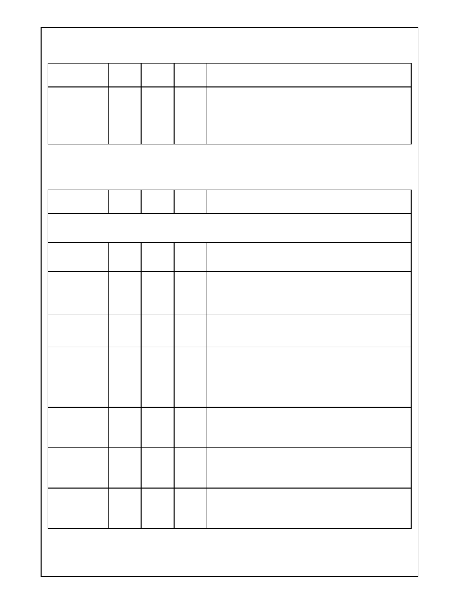
Revision 3.1
29
www.national.com
Signal Definitions (
Continued
)
GeodeTM
G
Xm
P
r
ocessor
GNT[2:0]#
E1,
F2,
D1
H2,
K4,
F2
O
Grant Lines
Grant indicates to the requesting master that it has been granted
access to the bus. Each master has its own GNT# line. GNT#
can be pulled away at any time a higher REQ# is received or if
the master does not begin a cycle within a minimum period of
time (16 SYSCLKs).
2.2.2
PCI Interface Signals (Continued)
Signal Name
BGA
Pin No.
SPGA
Pin No
Type
Description
2.2.3
Memory Controller Interface Signals
Signal Name
BGA
Pin No.
SPGA
Pin No.
Type
Description
Note:
The memory controller interface supports two types of memory configurations: SDRAM modules on the sys-
tem board and JEDEC DIMM connectors. Refer to Section 4.3 "Memory Controller" on page 103 for detailed
information regarding signal connections.
MD[63:0]
Refer
to Table
2-3
Refer
to Table
2-5
I/O
Memory Data Bus
The data bus lines driven to/from system memory.
MA[12:0]
Refer
to Table
2-3
Refer
to Table
2-5
O
Memory Address Bus
The multiplexed row/column address lines driven to the system
memory.
Supports 256 Mbit SDRAM.
BA[1:0]
AD26,
AD25
AJ33,
AK36
O
Bank Address Bits
These bits are used to select the component bank within the
SDRAM.
CS[3:0]#
AE23,
V25,
AD23,
V26
AK32,
Z34,
AN33,
AA35
O
Chip Selects
The chip selects are used to select the module bank within the
system memory. Each chip select corresponds to a specific mod-
ule bank.
If CS# is high, the bank(s) do not respond to RAS#, CAS#, WE#
until the bank is selected again.
RASA#,
RASB#
W24,
W25
AB36,
AB34
O
Row Address Strobe
RAS#, CAS#, WE# and CKE are encoded to support the differ-
ent SDRAM commands. RASA# is used with CS[1:0]#. RASB#
is used with CS[3:2]#.
CASA#,
CASB#
P25,
R26
W37,
X36
O
Column Address Strobe
RAS#, CAS#, WE# and CKE are encoded to support the differ-
ent SDRAM commands. CASA# is used with CS[1:0]#. CASB#
is used with CS[3:2]#.
WEA#,
WEB#
R25,
R24
W33,
W35
O
Write Enable
RAS#, CAS#, WE# and CKE are encoded to support the differ-
ent SDRAM commands. WEA# is used with CS[1:0]#. WEB# is
used with CS[3:2]#.

www.national.com
30
Revision 3.1
Signal Definitions (
Continued
)
GeodeTM
G
Xm
Pr
ocessor
DQM[7:0]
Refer
to Table
2-3
Refer
to Table
2-5
O
Data Mask Control Bits
During memory read cycles, these outputs control whether the
SDRAM output buffers are driven on the MD bus or not. All DQM
signals are asserted during read cycles.
During memory write cycles, these outputs control whether or
not MD data will be written into the SDRAM.
DQM[7:0] connect directly to the DQM7-0 pins of each connec-
tor.
CKEA,
CKEB
AF24,
AD16
AL33,
AN23
O
Clock Enable
For normal operation CKE is held high. CKE goes low during
Suspend.
SDCLK[3:0]
AE4,
AF5,
AE5,
AF4
AM8,
AK10,
AL7,
AK8
O
SDRAM Clocks
The SDRAM samples all the control, address, and data using
these clocks.
SDCLK_IN
AE8
AK12
I
SDRAM Clock Input
The GXm processor samples the memory read data on this
clock. Works in conjunction with the SDCLK_OUT signal.
SDCLK_OUT
AF8
AL13
O
SDRAM Clock Output
This output is routed back to SDCLK_IN. The board designer
should vary the length of the board trace to control skew
between SDCLK_IN and SDCLK.
2.2.3
Memory Controller Interface Signals (Continued)
Signal Name
BGA
Pin No.
SPGA
Pin No.
Type
Description
2.2.4
Video Interface Signals
Signal Name
BGA
Pin No
SPGA
Pin No
Type
Description
PCLK
AC1
AJ1
O
Pixel Port Clock
Pixel Port Clock represents the pixel dotclock or a 2x multiple of
the dotclock for some 16-bit-per-pixel modes. It determines the
data transfer rate from the GXm processor to the CS5530.
VID_CLK
P1
V4
O
Video Clock
Video Clock represents the video port clock to the CS5530. This
pin is only used if the Video Port is enabled.
DCLK
AB1
AD4
I
DOT Clock
The DCLK input is driven from the CS5530 and represents the
pixel dot clock. In some cases, such as when displaying 16 BPP
data with an eight-bit-graphics pixel port, this clock will actually
be a 2x multiple of the dotclock.
CRT_HSYNC
W2
AD2
O
CRT Horizontal Sync
CRT Horizontal Sync establishes the line rate and horizontal
retrace interval for an attached CRT. The polarity is programma-
ble and depends on the display mode.

Revision 3.1
31
www.national.com
Signal Definitions (
Continued
)
GeodeTM
G
Xm
P
r
ocessor
CRT_VSYNC
AA3
AH2
O
CRT Vertical Sync
CRT Vertical Sync establishes the screen refresh rate and verti-
cal retrace interval for an attached CRT. The polarity is program-
mable and depends on the display mode.
FP_HSYNC
L2
R4
O
Flat Panel Horizontal Sync
Flat Panel Horizontal Sync establishes the line rate and horizon-
tal retrace interval for a TFT display. Polarity is programmable
and depends on the display mode.
This signal is an input to the CS5530. The CS5530 re-drives this
signal to the flat panel.
If no flat panel is used in the system, this signal does not need to
be connected.
FP_VSYNC
J1
P2
O
Flat Panel Vertical Sync
Flat Panel Vertical Sync establishes the screen refresh rate and
vertical retrace interval for a TFT display. Polarity is programma-
ble and depends on the display mode.
This signal is an input to the CS5530. The CS5530 re-drives this
signal to the flat panel.
If no flat panel is used in the system, this signal does not need to
be connected.
ENA_DISP
AD5
AM6
O
Display Enable
Display Enable indicates the active display portion of a scan line
to the CS5530.
In a CS5530-based system, this signal is required to be con-
nected even if there is no TFT panel in the system.
VID_RDY
AD1
AK2
I
Video Ready
This input signal indicates that the video FIFO in the CS5530 is
ready to receive more data.
VID_VAL
M2
S3
O
Video Valid
VID_VAL qualifies valid video data to the CS5530.
VID_DATA[7:0]
Refer
to
Refer
to Table
2-5
O
Video Data Bus
When the Video Port is enabled, this bus drives Video (Y-U-V)
data synchronous to the VID_CLK output.
PIXEL[17:0]
Refer
to Table
2-3
Refer
to Table
2-5
O
Graphics Pixel Data Bus
This bus drives graphics pixel data synchronous to the PCLK
output.
2.2.4
Video Interface Signals (Continued)
Signal Name
BGA
Pin No
SPGA
Pin No
Type
Description

www.national.com
32
Revision 3.1
Signal Definitions (
Continued
)
GeodeTM
G
Xm
Pr
ocessor
2.2.5
Power, Ground, and No Connect Signals
Signal Name
BGA
Pin No.
SPGA
Pin No.
Type
Description
VOLDET
AC5
AM36
O
Voltage Detect
In early schematic revisions this pin was identified as VOLDET.
However, in the production version this pin is a "no connect" and
should be left disconnected.
VSS
Refer
to Table
2-3
(Total
of 71)
Refer
to Table
2-5
(Total
of 50)
GND
Ground Connection
VCC2
Refer
to Table
2-3
(Total
of 32)
Refer
to Table
2-5
(Total
of 32)
PWR
2.9V (nominal) Core Power Connection
VCC3
Refer
to Table
2-3
(Total
of 32)
Refer
to Table
2-5
(Total
of 18)
PWR
3.3V (nominal) I/O Power Connection
NC
--
Q5, X2,
Z2
No Connection
A line designated as NC should be left disconnected.
2.2.6
Internal Test and Measurement Signals
Signal Name
BGA
Pin No.
SPGA
Pin No.
Type
Description
FLT#
AC2
AJ3
I
Float
Float Outputs force the GXm processor to float all outputs in the
high-impedance state and to enter a power-down state.
RW_CLK
AE6
AL11
O
Raw Clock
This output is the GXm processor clock. This debug signal can
be used to verify clock operation.
TEST[3:0]
B22,
A23,
B21,
C21
D28,
B32,
D26,
A33
O
SDRAM Test Outputs
These outputs are used for internal debug only.
TCLK
J2
(PU)
P4
(PU)
I
Test Clock
JTAG test clock.
This pin is internally connected to a 20-kohm pull-up resistor.
TDI
D2
(PU)
F4
(PU)
I
Test Data Input
JTAG serial test-data input.
This pin is internally connected to a 20-kohm pull-up resistor.
TDO
F1
J1
O
Test Data Output
JTAG serial test-data output.

Revision 3.1
33
www.national.com
Signal Definitions (
Continued
)
GeodeTM
G
Xm
P
r
ocessor
TMS
H1
(PU)
N3
(PU)
I
Test Mode Select
JTAG test-mode select.
This pin is internally connected to a 20-kohm pull-up resistor.
TEST
F3
(PD)
J5
(PD)
I
Test
Test-mode input.
This pin is internally connected to a 20-kohm pull-down resistor.
TDP
E24
F36
O
Thermal Diode Positive
TDP is the positive terminal of the thermal diode on the die. The
diode is used to do thermal characterization of the device in a
system. This signal works in conjunction with TDN.
TDN
D26
E37
O
Thermal Diode Negative
TDN is the negative terminal of the thermal diode on the die. The
diode is used to do thermal characterization of the device in a
system. This signal works in conjunction with TDP.
2.2.6
Internal Test and Measurement Signals
Signal Name
BGA
Pin No.
SPGA
Pin No.
Type
Description
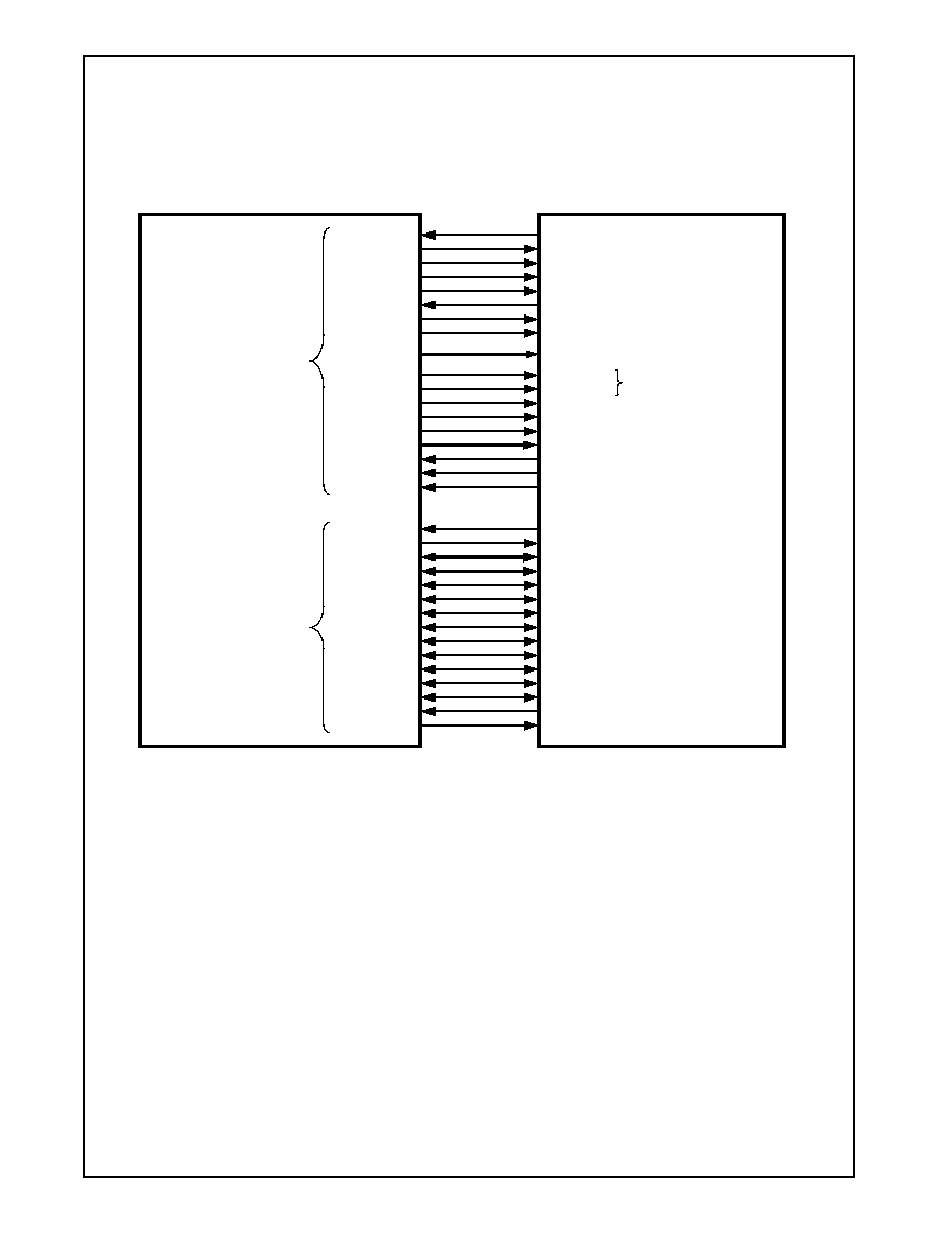
www.national.com
34
Revision 3.1
Signal Definitions (
Continued
)
GeodeTM
G
Xm
Pr
ocessor
2.3
SUBSYSTEM SIGNAL CONNECTIONS
As previously stated, the GXm Integrated Subsystem with
MMX support consists of two chips: the GXm Processor
and the CS5530 I/O companion. Figure 2-4 shows the
signal connections between the processor and the I/O
companion chip.
Figure 2-4. Subsystem Signal Connections
SYSCLK
SERIALP
IRQ13
SMI#
PCLK
CRT_HSYNC
CRT_VSYNC
PIXEL[17:0]
FP_HSYNC
FP_VSYNC
ENA_DISP
VID_VAL
VID_CLK
VID_DATA[7:0]
VID_RDY
INTR
SUSP#
SUSPA#
AD[31:0]
C/BE[3:0]#
PAR
FRAME#
IRDY#
TRDY#
STOP#
LOCK#
DEVSEL#
PERR#
SERR#
REQ0#
GX_CLK
PSERIAL
IRQ13
SMI#
PCLK
HSYNC
VSYNC
PIXEL[23:0]
FP_HSYNC
FP_VSYNC
FP_ENA_DISP
VID_VAL
VID_CLK
VID_DATA[7:0]
VID_RDY
CPU_RST
INTR
SUSP#
SUSPA#
AD[31:0]
C/BE[3:0]#
PAR
FRAME#
IRDY#
TRDY#
STOP#
LOCK#
DEVSEL#
PERR#
SERR#
REQ#
GNT#
GNT0#
GeodeTM CS5530
I/O Companion
Exclusive
Interconnect
Signals
(Do not connect to
any other device)
Nonexclusive
Interconnect
Signals
(May also connect
to other circuitry)
Not needed if
CRT only (no TFT)
(Note)
Note:
Refer to Figure 2-5 for interconnection of these lines.
RESET
DCLK
DCLK
GeodeTM GXm
Processor
Revision 3.1
35
www.national.com
Signal Definitions (
Continued
)
GeodeTM
G
Xm
P
r
ocessor
Figure 2-5. PIXEL Signal Connections
PIXEL17
PIXEL16
PIXEL15
PIXEL14
PIXEL13
PIXEL12
PIXEL11
PIXEL10
PIXEL9
PIXEL8
PIXEL7
PIXEL6
PIXEL5
PIXEL4
PIXEL3
PIXEL2
PIXEL1
GeodeTM CS5530
I/O Companion
PIXEL0
PIXEL23
PIXEL22
PIXEL21
PIXEL20
PIXEL19
PIXEL18
PIXEL17
PIXEL16
PIXEL15
PIXEL14
PIXEL13
PIXEL12
PIXEL11
PIXEL10
PIXEL9
PIXEL8
PIXEL7
PIXEL6
PIXEL5
PIXEL4
PIXEL3
PIXEL2
PIXEL1
PIXEL0
GeodeTM GXm
Processor

www.national.com
36
Revision 3.1
Signal Definitions (
Continued
)
GeodeTM
G
Xm
Pr
ocessor
2.4
POWER PLANES
Figure 2-6 shows layout recommendations for splitting the
power plane between VCC2 (core: 2.9V) and VCC3 (I/O:
3.3V) volts in the BGA package.
The illustration assumes there is one power plane, and no
components on the back of the board
Figure 2-7 shows layout recommendations for splitting the
power plane between VCC2 (core: 2.9V) and VCC3 (I/O:
3.3V) volts for the GXm in the SPGA package.
Figure 2-6. BGA Recommended Split Power Plane and Decoupling
1
26
A
AF
AF
A
26
1
= High frequency capacitor
= 220µF, low ESR capacitor
= 3.3V connection
= 2.9V connection
GeodeTM GXm
352 BGA - Top View
2.9V Plane
(VCC2)
3.3V Plane
(VCC3)
3.3V Plane
(VCC3)
3.3V Plane
(VCC3)
2.9V Plane
(VCC2)
Legend
Processor
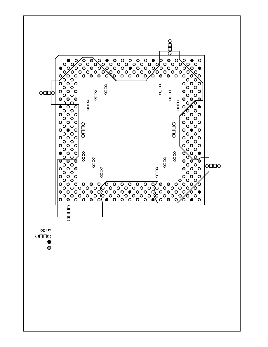
Revision 3.1
37
www.national.com
Signal Definitions (
Continued
)
GeodeTM
G
Xm
P
r
ocessor
Figure 2-7. SPGA Recommended Split Power Plane and Decoupling
1
37
A
AN
A
AN
1
37
2.9V Plane
(VCC2)
3.3V Plane
(VCC3)
3.3V Plane
(VCC3)
3.3V Plane
(VCC3)
3.3V Plane
(VCC3)
2.9V Plane
(VCC2)
To 2.9V
Regulator
Note: Where signals cross plane splits, it is recommended to include AC
decoupling between planes with 47pF capacitors.
= High frequency capacitor
= 220 µF, low ESR capacitor
= 3.3V connection
= 2.9V connection
Legend
320 SPGA - Top View
GeodeTM GXm
Processor
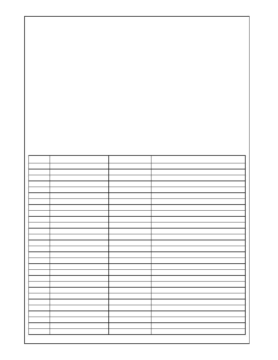
www.national.com
38
Revision 3.1
GeodeTM
G
Xm
Pr
ocessor
3.0
Processor Programming
This section describes the internal operations of the
Geode GXm processor from a programmer's point of view.
It includes a description of the traditional "core" process-
ing and FPU operations. The integrated function registers
are described at the end of this chapter.
The primary register sets within the processor core
include:
∑ Application Register Set
∑ System Register Set
∑ Model Specific Register Set
∑ Floating Point Unit Register Set.
The initialization of the major registers within in core are
shown in Table 3-1.
The integrated function sets are located in main memory
space and include:
∑ Internal Bus Interface Unit Register Set
∑ Graphics Pipeline Register Set
∑ Display Controller Register Set
∑ Memory Controller Register Set
∑ Power Management Register Set
3.1
CORE PROCESSOR INITIALIZATION
The GXm processor is initialized when the RESET signal
is asserted. The processor is placed in real mode and the
registers listed in Table 3-1 are set to their initialized val-
ues. RESET invalidates and disables the CPU cache, and
turns off paging. When RESET is asserted, the CPU ter-
minates all local bus activity and all internal execution.
During the entire time that RESET is asserted, the inter-
nal pipeline is flushed and no instruction execution or bus
activity occurs.
Approximately 150 to 250 external clock cycles after
RESET is deasserted, the processor begins executing
instructions at the top of physical memory (address loca-
tion FFFFFFF0h). The actual time depends on the clock
scaling in use. Also, an additional 2
20
clock cycles are
needed when self-test is requested.
Typically, an intersegment jump is placed at FFFFFFF0h.
This instruction will force the processor to begin execution
in the lowest 1 MB of address space.
The following table, Table 3-1, lists the core registers and
illustrates how they are initialized.
Table 3-1. Initialized Core Register Controls
Register
Register Name
Initialized Contents
Comments
EAX
Accumulator
xxxxxxxxh
00000000h indicates self-test passed.
EBX
Base
xxxxxxxxh
ECX
Count
xxxxxxxxh
EDX
Data
xxxx 04 [DIR0]h
DIR0 = Device ID
EBP
Base Pointer
xxxxxxxxh
ESI
Source Index
xxxxxxxxh
EDI
Destination Index
xxxxxxxxh
ESP
Stack Pointer
xxxxxxxxh
EFLAGS
Extended FLAGS
00000002h
See Table 3-4 on page 43 for bit definitions.
EIP
Instruction Pointer
0000FFF0h
ES
Extra Segment
0000h
Base address set to 00000000h. Limit set to FFFFh.
CS
Code Segment
F000h
Base address set to FFFF0000h. Limit set to FFFFh.
SS
Stack Segment
0000h
Base address set to 00000000h. Limit set to FFFFh.
DS
Data Segment
0000h
Base address set to 00000000h. Limit set to FFFFh.
FS
Extra Segment
0000h
Base address set to 00000000h. Limit set to FFFFh.
GS
Extra Segment
0000h
Base address set to 00000000h. Limit set to FFFFh.
IDTR
Interrupt Descriptor Table Register
Base = 0, Limit = 3FFh
GDTR
Global Descriptor Table Register
xxxx xxxxh
LDTR
Local Descriptor Table Register
xxxxh
TR
Task Register
xxxxh
CR0
Machine Status Word
60000010h
See Table 3-7 on page 49 for bit definitions.
CR2
Control Register 2
xxxxxxxxh
See Table 3-7 on page 49 for bit definitions.
CR3
Control Register 3
xxxxxxxxh
See Table 3-7 on page 49 for bit definitions.
CR4
Control Register 4
00000000h
See Table 3-7 on page 49 for bit definitions.
CCR1
Configuration Control 1
00h
See Table 3-11 on page 49 for bit definitions.
CCR2
Configuration Control 2
00h
See Table 3-11 on page 49 for bit definitions.
CCR3
Configuration Control 3
00h
See Table 3-11 on page 49 for bit definitions.
CCR7
Configuration Control 7
00h
See Table 3-11 on page 50 for bit definitions.
SMAR0
SMM Address 0
00h
See Table 3-11 on page 51 for bit definitions.

Revision 3.1
39
www.national.com
Processor Programming (
Continued
)
GeodeTM
G
Xm
P
r
ocessor
3.2
INSTRUCTION SET OVERVIEW
The GXm processor instruction set can be divided into
nine types of operations:
∑ Arithmetic
∑ Bit Manipulation
∑ Shift/Rotate
∑ String Manipulation
∑ Control Transfer
∑ Data Transfer
∑ Floating Point
∑ High-Level Language Support
∑ Operating System Support
GXm processor instructions operate on as few as zero
operands and as many as three operands. An NOP
instruction (no operation) is an example of a zero-operand
instruction. Two-operand instructions allow the specifica-
tion of an explicit source and destination pair as part of
the instruction. These two-operand instructions can be
divided into ten groups according to operand types:
∑ Register to Register
∑ Register to Memory
∑ Memory to Register
∑ Memory to Memory
∑ Register to I/O
∑ I/O to Register
∑ Memory to I/O
∑ I/O to Memory
∑ Immediate Data to Register
∑ Immediate Data to Memory
An operand can be held in the instruction itself (as in the
case of an immediate operand), in one of the processor's
registers or I/O ports, or in memory. An immediate oper-
and is fetched as part of the opcode for the instruction.
Operand lengths of 8, 16, 32 or 48 bits are supported as
well as 64 or 80 bits associated with floating-point instruc-
tions. Operand lengths of 8 or 32 bits are generally used
when executing code written for 386- or 486-class (32-bit
code) processors. Operand lengths of 8 or 16 bits are
generally used when executing existing 8086 or 80286
code (16-bit code). The default length of an operand can
be overridden by placing one or more instruction prefixes
in front of the opcode. For example, the use of prefixes
allows a 32-bit operand to be used with 16-bit code or a
16-bit operand to be used with 32-bit code.
Section 9.1 "General Instruction Set Format" on page 202
contains the clock count table that lists each instruction in
the CPU instruction set. Included in the table are the
associated opcodes, execution clock counts, and effects
on the EFLAGS register.
3.2.1
Lock Prefix
The LOCK prefix may be placed before certain instruc-
tions that read, modify, then write back to memory. The
PCI will not be granted access in the middle of locked
instructions. The LOCK prefix can be used with the follow-
ing instructions only when the result is a write operation to
memory.
∑ Bit Test Instructions (BTS, BTR, BTC)
∑ Exchange Instructions (XADD, XCHG, CMPXCHG)
∑ One-Operand Arithmetic and Logical Instructions
(DEC, INC, NEG, NOT)
∑ Two-Operand Arithmetic and Logical Instructions
(ADC, ADD, AND, OR, SBB, SUB, XOR).
An invalid opcode exception is generated if the LOCK pre-
fix is used with any other instruction or with one of the
instructions above when no write operation to memory
occurs (for example, when the destination is a register).
SMAR1
SMM Address 1
00h
See Table 3-11 on page 50 for bit definitions.
SMAR2
SMM Address 2 / SMAR Size
00h
See Table 3-11 on page 50 for bit definitions.
DIR0
Device Identification 0
4xh
Device ID and reads back initial CPU clock-speed set-
ting. See Table 3-11 on page 51 for bit definitions.
DIR1
Device Identification 1
xxh
Stepping and Revision ID (RO). See Table 3-11 on
page 51 for bit definitions.
DR7
Debug Register 7
00000400h
See Table 3-13 on page 53 for bit definitions.
Note: x = Undefined value
Table 3-1. Initialized Core Register Controls (Continued)
Register
Register Name
Initialized Contents
Comments

www.national.com
40
Revision 3.1
Processor Programming (
Continued
)
GeodeTM
G
Xm
Pr
ocessor
3.3
REGISTER SETS
The accessible registers in the processor are grouped into
three sets:
1)
The Application Register Set contains the registers
frequently used by application programmers. Table 3-
2 shows the general purpose, segment, the instruc-
tion pointer and the EFLAGS Registers.
2)
The System Register Set contains the registers typi-
cally reserved for operating-systems programmers:
control, system address, debug, configuration, and
test registers.
3)
The Model Specific Register (MSR) Set is used to
monitor the performance of the processor or a
specific component within the processor. The model
specific register set has one 64-bit register called the
Time Stamp Counter.
Each of these register sets are discussed in detail in the
subsections that follow. Additional registers to support
integrated GXm processor subsystems are described in
Section 4.1 "Integrated Functions Programming Interface"
on page 92.
3.3.1
Application Register Set
The Application Register Set consists of the registers most
often used by the applications programmer. These regis-
ters are generally accessible, although some bits in the
EFLAGS register are protected.
The General Purpose Register contents are frequently
modified by instructions and typically contain arithmetic
and logical instruction operands.
In real mode, Segment Registers contain the base
address for each segment. In protected mode, the seg-
ment registers contain segment selectors. The segment
selectors provide indexing for tables (located in memory)
that contain the base address for each segment, as well
as other memory addressing information.
The Instruction Pointer Register points to the next
instruction that the processor will execute. This register is
automatically incremented by the processor as execution
progresses.
The EFLAGS Register contains control bits used to
reflect the status of previously executed instructions. This
register also contains control bits that affect the operation
of some instructions.
3.3.1.1
General Purpose Registers
The General Purpose Registers are divided into four data
registers, two pointer registers, and two index registers as
shown in Table 3-2.
The Data Registers are used by the applications pro-
grammer to manipulate data structures and to hold the
results of logical and arithmetic operations. Different por-
tions of general data registers can be addressed by using
different names.
An "E" prefix identifies the complete 32-bit register. An "X"
suffix without the "E" prefix identifies the lower 16 bits of
the register.
The lower two bytes of a data register are addressed with
an "H" suffix (identifies the upper byte) or an "L" suffix (iden-
tifies the lower byte). These _L and _H portions of the
data registers act as independent registers. For example,
if the AH register is written to by an instruction, the AL reg-
ister bits remain unchanged.
The Pointer and Index Registers are listed below.
SI or ESI
Source Index
DI or EDI
Destination Index
SP or ESP
Stack Pointer
BP or EBP
Base Pointer
These registers can be addressed as 16- or 32-bit registers,
with the "E" prefix indicating 32 bits. The pointer and index
registers can be used as general purpose registers; how-
ever, some instructions use a fixed assignment of these
registers. For example, repeated string operations always
use ESI as the source pointer, EDI as the destination
pointer, and ECX as a counter. The instructions that use
fixed registers include multiply and divide, I/O access,
string operations, stack operations, loop, variable shift and
rotate, and translate instructions.
The GXm processor implements a stack using the ESP
register. This stack is accessed during the PUSH and
POP instructions, procedure calls, procedure returns,
interrupts, exceptions, and interrupt/exception returns.
The GXm processor automatically adjusts the value of the
ESP during operations that result from these instructions.
The EBP register may be used to refer to data passed on
the stack during procedure calls. Local data may also be
placed on the stack and accessed with BP. This register
provides a mechanism to access tack data in high-level
languages.

Revision 3.1
41
www.national.com
Processor Programming (
Continued
)
GeodeTM
G
Xm
P
r
ocessor
Table 3-2. Application Register Set
31 30 29 28 27 26 25 24 23 22 21 20 19 18 17 16 15 14 13 12 11 10
9
8
7
6
5
4
3
2
1
0
General Purpose Registers
AX
AH
AL
EAX (Extended A Register)
BX
BH
BL
EBX (Extended B Register)
CX
CH
CL
ECX (Extended C Register)
DX
DH
DL
EDX (Extended D Register)
SI (Source Index)
ESI (Extended Source Index)
DI (Destination Index)
EDI (Extended Destination Index)
BP (Base Pointer)
EBP (Extended Base Pointer)
SP (Stack Pointer)
ESP (Extended Stack Pointer)
Segment (Selector) Registers
CS (Code Segment)
SS (Stack Segment)
DS (D Data Segment)
ES (E Data Segment)
FS (F Data Segment)
GS (G Data Segment)
Instruction Pointer and EFLAGS Registers
EIP (Extended Instruction Pointer)
ESP (Extended FLAGS Register)

www.national.com
42
Revision 3.1
Processor Programming (
Continued
)
GeodeTM
G
Xm
Pr
ocessor
3.3.1.2
Segment Registers
The 16-bit segment registers, part of the main memory
addressing mechanism, are described in Section 3.5 "Off-
set, Segment, and Paging Mechanisms" on page 61. The
six segment registers are:
CS
-
Code Segment
DS
-
Data Segment
SS
-
Stack Segment
ES
-
Extra Segment
FS
-
Additional Data Segment
GS
-
Additional Data Segment
The segment registers are used to select segments in
main memory. A segment acts as private memory for dif-
ferent elements of a program such as code space, data
space, and stack space.
There are two segment mechanisms, one for real and vir-
tual 8086 operating modes and one for protective mode.
Initialization and transition to protective mode is described
in Section 3.13.4 "Initialization and Transition to Protected
Mode" on page 87. The segment mechanisms are
described in Section 3.7 "Descriptors and Segment Mech-
anisms" on page 62.
The active segment register is selected according to the
rules listed in Table 3-3 and the type of instruction being
currently processed. In general, the DS register selector is
used for data references. Stack references use the SS
register, and instruction fetches use the CS register. While
some of these selections may be overridden, instruction
fetches, stack operations, and the destination write opera-
tion of string operations cannot be overridden. Special
segment-override instruction prefixes allow the use of
alternate segment registers. These segment registers
include the ES, FS, and GS registers.
3.3.1.3
Instruction Pointer Register
The Instruction Pointer (EIP) Register contains the off-
set into the current code segment of the next instruction to
be executed. The register is normally incremented by the
length of the current instruction with each instruction exe-
cution unless it is implicitly modified through an interrupt,
exception, or an instruction that changes the sequential
execution flow (for example JMP and CALL).
Table 3-3 illustrates the code segment selection rules.
Table 3-3. Segment Register Selection Rules
Type of Memory Reference
Implied (Default)
Segment
Segment-Override
Prefix
Code Fetch
CS
None
Destination of PUSH, PUSHF, INT, CALL, PUSHA instructions
SS
None
Source of POP, POPA, POPF, IRET, RET instructions
SS
None
Destination of STOS, MOVS, REP STOS, REP MOVS instructions
ES
None
Other data references with effective address using base registers of:
EAX, EBX, ECX, EDX, ESI, EDI, EBP, ESP
DS
SS
CS, ES, FS, GS, SS
CS, DS, ES, FS, GS
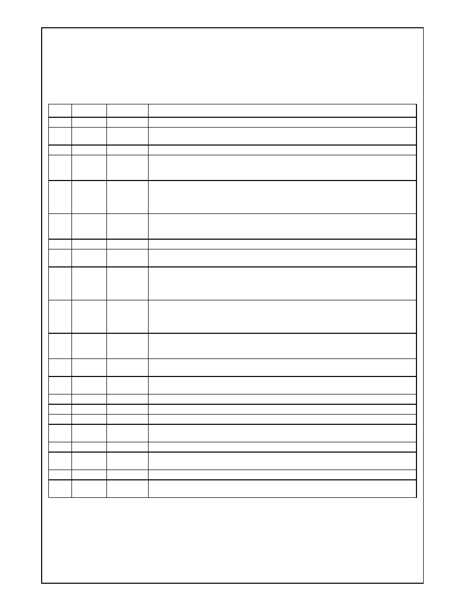
Revision 3.1
43
www.national.com
Processor Programming (
Continued
)
GeodeTM
G
Xm
P
r
ocessor
3.3.1.4
EFLAGS Register
The EFLAGS Register contains status information and
controls certain operations on the GXm processor. The
lower 16 bits of this register are referred to as the
EFLAGS register that is used when executing 8086 or
80286 code. Table 3-4 gives the bit formats for the
EFLAGS Register
Table 3-4. EFLAGS Register
Bit
Name
Flag Type
Description
31:22
RSVD
--
Reserved: Set to 0.
21
ID
System
Identification Bit: The ability to set and clear this bit indicates that the CPUID instruction is sup-
ported. The ID can be modified only if the CPUID bit in CCR4 (Index E8h[7]) is set.
20:19
RSVD
--
Reserved: Set to 0.
18
AC
System
Alignment Check Enable: In conjunction with the AM flag (bit 18) in CR0, the AC flag deter-
mines whether or not misaligned accesses to memory cause a fault. If AC is set, alignment faults
are enabled.
17
VM
System
Virtual 8086 Mode: If set while in protected mode, the processor switches to virtual 8086 opera-
tion handling segment loads as the 8086 does, but generating exception 13 faults on privileged
opcodes. The VM bit can be set by the IRET instruction (if current privilege level
is 0) or by task switches at any privilege level.
16
RF
Debug
Resume Flag: Used in conjunction with debug register breakpoints. RF is checked at instruction
boundaries before breakpoint exception processing. If set, any debug fault is ignored on the next
instruction.
15
RSVD
--
Reserved: Set to 0.
14
NT
System
Nested Task: While executing in protected mode, NT indicates that the execution of the current
task is nested within another task.
13:12
IOPL
System
I/O Privilege Level: While executing in protected mode, IOPL indicates the maximum current
privilege level (CPL) permitted to execute I/O instructions without generating an exception 13
fault or consulting the I/O permission bit map. IOPL also indicates the maximum CPL allowing
alteration of the IF bit when new values are popped into the EFLAGS register.
11
OF
Arithmetic
Overflow Flag: Set if the operation resulted in a carry or borrow into the sign bit of the result but
did not result in a carry or borrow out of the high-order bit. Also set if the operation resulted in a
carry or borrow out of the high-order bit but did not result in a carry or borrow into the sign bit of
the result.
10
DF
Control
Direction Flag: When cleared, DF causes string instructions to auto-increment (default) the
appropriate index registers (ESI and/or EDI). Setting DF causes auto-decrement of the index
registers to occur.
9
IF
System
Interrupt Enable Flag: When set, maskable interrupts (INTR input pin) are acknowledged and
serviced by the CPU.
8
TF
Debug
Trap Enable Flag: Once set, a single-step interrupt occurs after the next instruction completes
execution. TF is cleared by the single-step interrupt.
7
SF
Arithmetic
Sign Flag: Set equal to high-order bit of result (0 indicates positive, 1 indicates negative).
6
ZF
Arithmetic
Zero Flag: Set if result is zero; cleared otherwise.
5
RSVD
--
Reserved: Set to 0.
4
AF
Arithmetic
Auxiliary Carry Flag: Set when a carry out of (addition) or borrow into (subtraction) bit position 3
of the result occurs; cleared otherwise.
3
RSVD
--
Reserved: Set to 0.
2
PF
Arithmetic
Parity Flag: Set when the low-order 8 bits of the result contain an even number of ones; other-
wise PF is cleared.
1
RSVD
Reserved: Set to 1.
0
CF
Arithmetic
Carry Flag: Set when a carry out of (addition) or borrow into (subtraction) the most significant bit
of the result occurs; cleared otherwise.
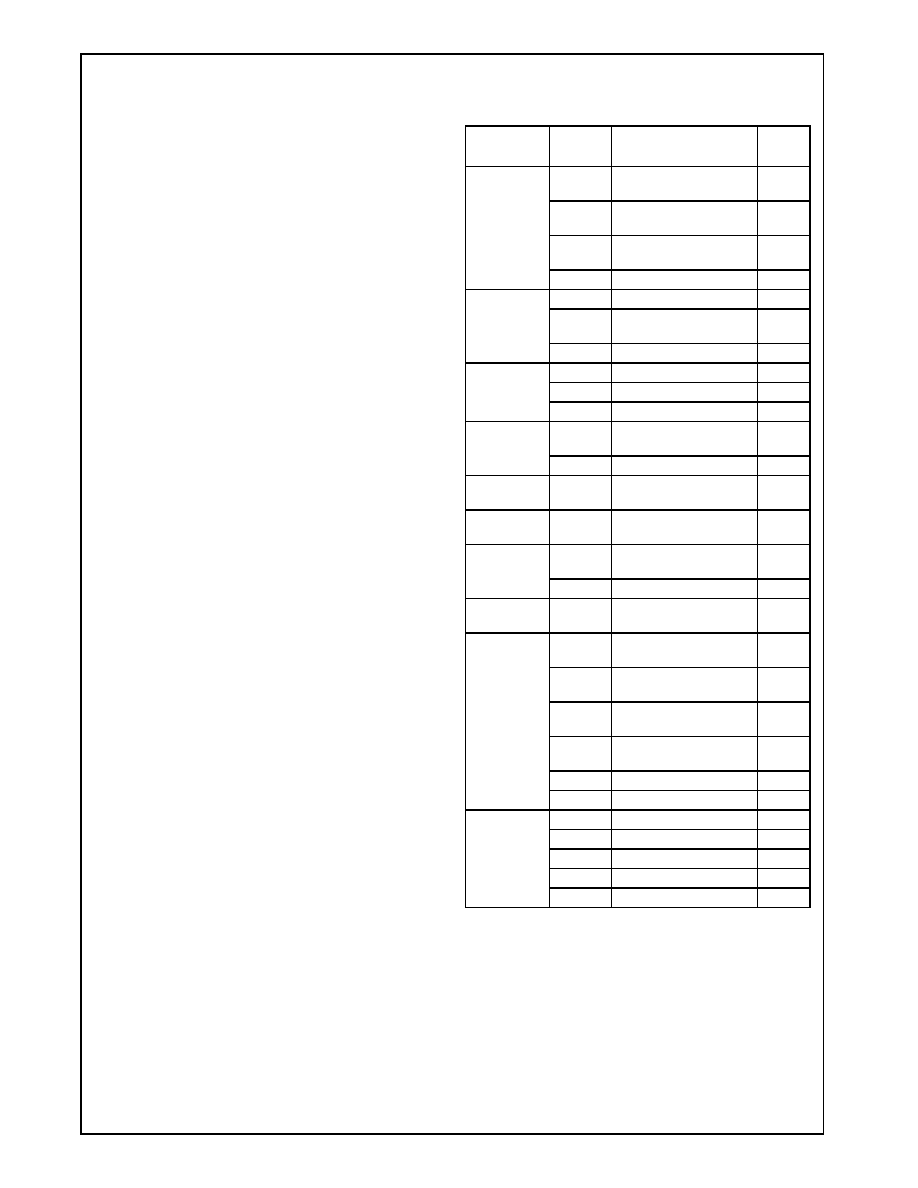
www.national.com
44
Revision 3.1
Processor Programming (
Continued
)
GeodeTM
G
Xm
Pr
ocessor
3.3.2
System Register Set
The system register set, shown in Table 3-5, consists of
registers not generally used by application programmers.
These registers are typically employed by system level
programmers who generate operating systems and mem-
ory management programs. Associated with the system
register set are certain tables and segments which are
listed in Table 3-5.
The Control Registers control certain aspects of the
GXm processor such as paging, coprocessor functions,
and segment protection.
The Descriptor Tables hold descriptors that manage
memory segments and tables, interrupts and task switch-
ing. The tables are defined by corresponding registers.
The two Task State Segments Tables defined by TSS reg-
ister are used to save and load the computer state when
switching tasks.
The Configuration Registers are used to define the
GXm CPU setup including cache management.
The ID registers allow BIOS and other software to identify
the specific CPU and stepping. System Management
Mode (SMM) control information is stored in the SMM reg-
isters.
The Debug Registers provide debugging facilities for the
GXm processor and enable the use of data access break-
points and code execution breakpoints.
The Test Registers provide a mechanism to test the con-
tents of both the on-chip 16 KB cache and the Translation
Lookaside Buffer (TLB). The TLB is used as a cache for
the tables that are used in to translate linear addresses to
physical addresses while paging is enabled.
Table 3-5 lists the system register sets along with their
size and function.
Table 3-5. System Register Set
Group
Name
Function
Width
(Bits)
Control
Registers
CR0
System Control
Register
32
CR2
Page Fault Linear
Address Register
32
CR3
Page Directory Base
Register
32
CR4
Time Stamp Counter
32
Descriptor
Tables
GDT
General Descriptor Table
32
IDT
Interrupt Descriptor
Table
32
LDT
Local Descriptor Table
16
Descriptor
Table
Registers
GDTR
GDT Register
32
IDTR
IDT Register
32
LDTR
LDT Register
16
Task State
Segment and
Registers
TSS
Task State Segment
Tables
16
TR
TSS Register Setup
16
Configuration
Registers
CCRn
Configuration Control
Registers
8
ID
Registers
DIRn
Device Identification
Registers
8
SMM
Registers
SMARn
SMM Address Region
Registers
8
SMHRn
SMM Header Addresses
8
Performance
Registers
PCR0
Performance Control
Register
8
Debug
Registers
DR0
Linear Breakpoint
Address 0
32
DR1
Linear Breakpoint
Address 1
32
DR2
Linear Breakpoint
Address 2
32
DR3
Linear Breakpoint
Address 3
32
DR6
Breakpoint Status
32
DR7
Breakpoint Control
32
Test
Registers
TR3
Cache Test
32
TR4
Cache Test
32
TR5
Cache Test
32
TR6
TLB Test Control
32
TR7
TLB Test Status
32
Revision 3.1
45
www.national.com
Processor Programming (
Continued
)
GeodeTM
G
Xm
P
r
ocessor
3.3.2.1
Control Registers
A map of the Control Registers (CR0, CR2, CR3, and
CR4) is shown in Table 3-6 and the bit definitions are given
in Table 3-7. (These registers should not be confused with
the CRRn registers.) The CR0 register contains system
control bits which configure operating modes and indicate
the general state of the CPU. The lower 16 bits of CR0 are
referred to as the Machine Status Word (MSW).
When operating in real mode, any program can read and
write the control registers. In protected mode, however,
only privilege level 0 (most-privileged) programs can read
and write these registers.
Table 3-6. Control Registers Map
31 30 29 28 27 26 25 24 23 22 21 20 19 18 17 16 15 14 13 12 11 10
9
8
7
6
5
4
3
2
1
0
CR4 Register
Control Register 4 (R/W)
RSVD
T
S
C
RSVD
CR3 Register
Control Register 3 (R/W)
PDBR (Page Directory Base Register)
RSVD
0
0
RSVD
CR2 Register
Control Register 2 (R/W)
PFLA (Page Fault Linear Address)
CR1 Register
Control Register 1 (R/W)
RSVD
CR0 Register
Control Register 0 (R/W)
P
G
C
D
N
W
RSVD
A
M
R
S
V
D
W
P
RSVD
N
E
R
S
V
D
T
S
E
M
M
P
P
E
Machine Status Word (MSW)
Table 3-7. CR4-CR0 Bit Definitions
Bit
Name
Description
CR4 Register
Control Register 4 (R/W)
31:3
RSVD
Reserved: Set to 0 (always returns 0 when read).
2
TSC
Time Stamp Counter Instruction:
If = 1 RDTSC instruction enabled for CPL = 0 only; reset state.
If = 0 RDTSC instruction enabled for all CPL states.
1:0
RSVD
Reserved: Set to 0 (always returns 0 when read).
CR3 Register
Control Register 3 (R/W)
31:12
PDBR
Page Directory Base Register: Identifies page directory base address on a 4 KB page boundary.
11:0
RSVD
Reserved: Set to 0.
CR2 Register
Control Register 2 (R/W)
31:0
PFLA
Page Fault Linear Address: With paging enabled and after a page fault, PFLA contains the linear address of the
address that caused the page fault.
CR1 Register
Control Register 1 (R/W)
31:0
RSVD
Reserved
CR0 Register
Control Register 0 (R/W)
31
PG
Paging Enable Bit: If PG = 1 and protected mode is enabled (PE = 1), paging is enabled. After changing the
state of PG, software must execute an unconditional branch instruction (e.g., JMP, CALL) to have the change
take effect.
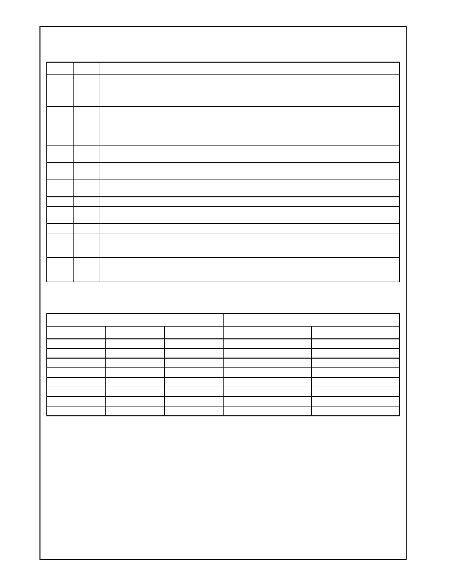
www.national.com
46
Revision 3.1
Processor Programming (
Continued
)
GeodeTM
G
Xm
Pr
ocessor
30
CD
Cache Disable: If CD = 1, no further cache line fills occur. However, data already present in the cache continues
to be used if the requested address hits in the cache. Writes continue to update the cache and cache invalida-
tions due to inquiry cycles occur normally. The cache must also be invalidated with a WBINVD instruction to com-
pletely disable any cache activity.
29
NW
Not Write-Through: If NW = 1, the on-chip cache operates in write-back mode. In write-back mode, writes are
issued to the external bus only for a cache miss, a line replacement of a modified line, execution of a locked
instruction, or a line eviction as the result of a flush cycle. If NW = 0, the on-chip cache operates in write-through
mode. In write-through mode, all writes (including cache hits) are issued to the external bus. This bit cannot be
changed if LOCK_NW = 1 in CCR2.
18
AM
Alignment Check Mask: If AM = 1, the AC bit in the EFLAGS register is unmasked and allowed to enable align-
ment check faults. Setting AM = 0 prevents AC faults from occurring.
16
WP
Write Protect: Protects read-only pages from supervisor write access. WP = 0 allows a read-only page to be
written from privilege level 0-2. WP = 1 forces a fault on a write to a read-only page from any privilege level.
5
NE
Numerics Exception: NE = 1 to allow FPU exceptions to be handled by interrupt 16. NE = 0 if FPU exceptions
are to be handled by external interrupts.
4
RSVD
Reserved: Do not attempt to modify, always 1.
3
TS
Task Switched: Set whenever a task switch operation is performed. Execution of a floating point instruction with
TS = 1 causes a DNA fault. If MP = 1 and TS = 1, a WAIT instruction also causes a DNA fault.
2
EM
Emulate Processor Extension: If EM = 1, all floating point instructions cause a DNA fault 7.
1
MP
Monitor Processor Extension: If MP = 1 and TS = 1, a WAIT instruction causes Device Not Available (DNA)
fault 7. The TS bit is set to 1 on task switches by the CPU. Floating point instructions are not affected by the state
of the MP bit. The MP bit should be set to one during normal operations.
0
PE
Protected Mode Enable: Enables the segment based protection mechanism. If PE = 1, protected mode is
enabled. If PE = 0, the CPU operates in real mode and addresses are formed as in an 8086-style CPU. Refer to
Section 3.13 "Protection" on page 86.
Table 3-7. CR4-CR0 Bit Definitions (Continued)
Bit
Name
Description
Table 3-8. Effects of Various Combinations of EM, TS, and MP Bits
CR0[3:1]
Instruction Type
TS
EM
MP
WAIT
ESC
0
0
0
Execute
Execute
0
0
1
Execute
Execute
1
0
0
Execute
Fault 7
1
0
1
Fault 7
Fault 7
0
1
0
Execute
Fault 7
0
1
1
Execute
Fault 7
1
1
0
Execute
Fault 7
1
1
1
Fault 7
Fault 7
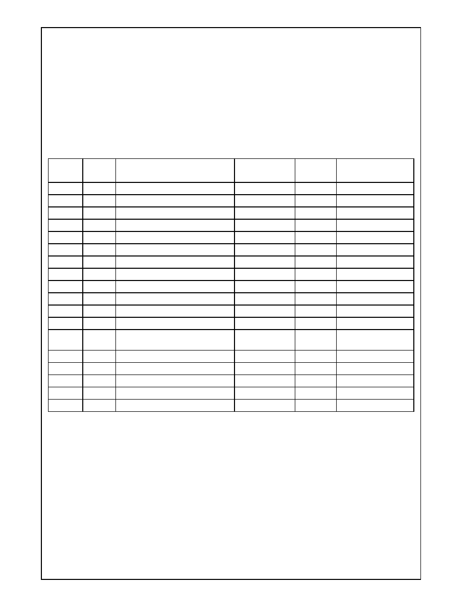
Revision 3.1
47
www.national.com
Processor Programming (
Continued
)
GeodeTM
G
Xm
P
r
ocessor
3.3.2.2
Configuration Registers
The configuration registers listed in Table 3-9 are CPU
registers and are selected by register index numbers. The
registers are accessed through I/O memory locations 22h
and 23h. Registers are selected for access by writing an
index number to I/O Port 22h using an OUT instruction
prior to transferring data through I/O Port 23h.
Each data transfer through I/O Port 23h must be preceded
by a register index selection through I/O Port 22h; other-
wise, subsequent I/O Port 23h operations are directed off-
chip and produce external I/O cycles.
If MAPEN, bit 4 of CCR3 (Index C3h[4]) = 0, external I/O
cycles occur if the register index number is outside the
range C0h-CFh, FEh, and FFh. The MAPEN bit should
remain 0 during normal operation to allow system regis-
ters located at I/O Port 22h to be accessed.
Table 3-9. Configuration Register Summary
Index
Type
Name
Access
Controlled By*
Default
Value
Reference
(Bit Formats)
C1h
R/W
CCR1 -- Configuration Control 1
SMI_LOCK
00h
Table 3-11 on page 49
C2h
R/W
CCR2 -- Configuration Control 2
--
00h
Table 3-11 on page 49
C3h
R/W
CCR3 -- Configuration Control 3
SMI_LOCK
00h
Table 3-11 on page 49
E8h
R/W
CCR4 -- Configuration Control 4
MAPEN
85h
Table 3-11 on page 50
EBh
R/W
CCR7 -- Configuration Control 7
--
00h
Table 3-11 on page 50
20h
R/W
PCR -- Performance Control
MAPEN
07h
Table 3-11 on page 50
B0h
R/W
SMHR0 -- SMM Header Address 0
MAPEN
xxh
Table 3-11 on page 50
B1h
R/W
SMHR1 -- SMM Header Address 1
MAPEN
xxh
Table 3-11 on page 50
B2h
R/W
SMHR2 -- SMM Header Address 2
MAPEN
xxh
Table 3-11 on page 50
B3h
R/W
SMHR3 -- SMM Header Address 3
MAPEN
xxh
Table 3-11 on page 50
B8h
R/W
GCR -- Graphics Control Register
MAPEN
00h
Table 4-1 on page 92
B9h
VGACTL -- VGA Control Register
--
00h
Table 5-5 on page 173
BAh-
BDh
VGAM0 -- VGA Mask Register
--
00h
Table 5-5 on page 173
CDh
R/W
SMAR0 -- SMM Address 0
SMI_LOCK
00h
Table 3-11 on page 51
CEh
R/W
SMAR1 -- SMM Address 1
SMI_LOCK
00h
Table 3-11 on page 51
CFh
R/W
SMAR2 -- SMM Address 2
SMI_LOCK
00h
Table 3-11 on page 51
FEh
RO
DIR0 -- Device ID 0
--
4xh
Table 3-11 on page 51
FFh
RO
DIR1 -- Device ID 1
--
xxh
Table 3-11 on page 51
Note:
*MAPEN = Index C3h[4] (CCR3) and SMI_LOCK = Index C3h[0] (CCR3).
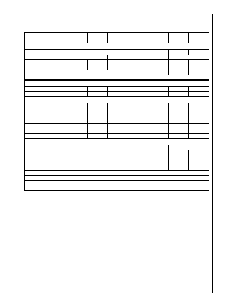
www.national.com
48
Revision 3.1
Processor Programming (
Continued
)
GeodeTM
G
Xm
Pr
ocessor
Table 3-10. Configuration Register Map
Register
(Index)
Bit 7
Bit 6
Bit 5
Bit 4
Bit 3
Bit 2
Bit 1
Bit 0
Control Registers
CCR1 (C1h)
RSVD
SMAC
USE_SMI
RSVD
CCR2 (C2h)
USE_SUSP
RSVD
WT1
SUSP_HLT
LOCK_NW
RSVD
CCR3 (C3h)
LSS_34
LSS_23
LSS_12
MAPEN
RSVD
NMI_EN
SMI_LOCK
CCR4 (E8h)
CPUID
SMI_NEST
RSVD
DTE_EN
MEM_BYP
IORT2
IORT1
IORT0
CCR7 (EBh)
RSVD
NMI
RSVD
EMMX
PCR (20h)
LSSER
RSVD
Device ID Registers
DIR0 (FEh)
DID3
DID2
DID1
DID0
RSVD
CLKMODE1
RSVD
CLMODE0
DIR1 (FFh)
SID3
SID2
SID1
SID0
RID3
RID2
RID1
RID0
SMM Base Header Address Registers
SMAR0 (CDh)
A31
A30
A29
A28
A27
A26
A25
A24
SMAR1 (CEh)
A23
A22
A21
A20
A19
A18
A17
A16
SMAR2 (CFh)
A15
A14
A13
A12
SIZE3
SIZE2
SIZE1
SIZE0
SMHR0 (B0h)
A7
A6
A5
A4
A3
A2
A1
A0
SMHR1 (B1h)
A15
A14
A13
A12
A11
A10
A9
A8
SMHR2 (B2h)
A23
A22
A21
A20
A19
A18
A17
A16
SMHR3 (B3h)
A31
A30
A29
A28
A27
A26
A26
A24
Graphics/VGA Related Registers
GCR (B8h)
RSVD
Scratchpad Size
Base Address Code
VGACTL (B9h)
RSVD
Enable SMI
for VGA
memory
B8000h to
BFFFFh
Enable SMI
for VGA
memory
B0000h to
B7FFFh
Enable SMI
for VGA
memory
A0000h to
AFFFFh
VGAM0 (BAh)
VGA Mask Register Bits [7:0]
VGAM1 (BBh)
VGA Mask Register Bits [15:8]
VGAM2 (BCh)
VGA Mask Register Bits [23:16]
VGAM3 (BDh)
VGA Mask Register Bits [31:24]
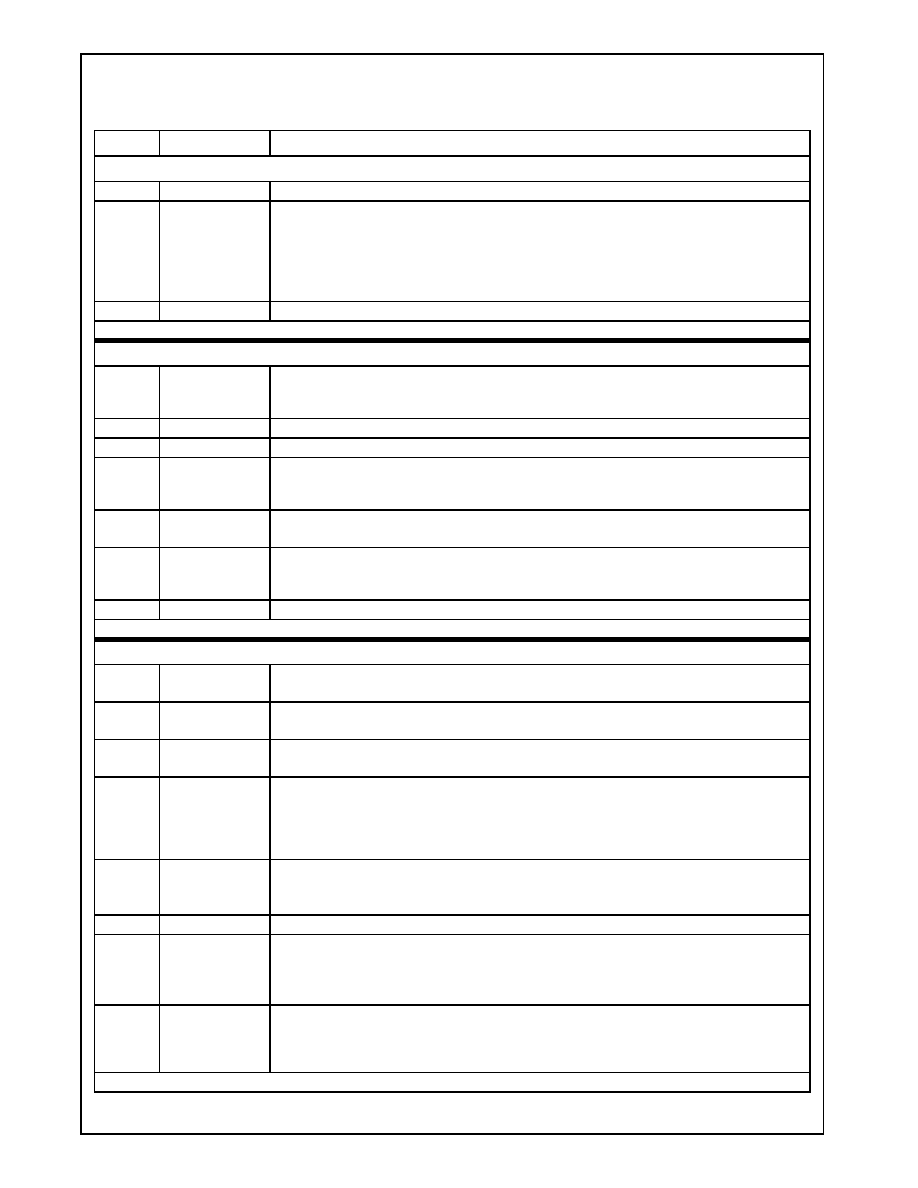
Revision 3.1
49
www.national.com
Processor Programming (
Continued
)
GeodeTM
G
Xm
P
r
ocessor
Table 3-11. Configuration Registers
Bit
Name
Description
Index C1h
CCR1 -- Configuration Control Register 1 (R/W)
Default Value = 00h
7:3
RSVD
Reserved: Set to 0.
2:1
SMAC
System Management Memory Access:
If = 00: SMM is disabled.
If = 01: SMI# pin is active to enter SMM. SMINT instruction is inactive.
If = 10: SMM is disabled.
If = 11: SMINT instruction is active to enter SMM. SMI# pin is inactive.
Note: SMI_LOCK (CCR3[0]) must = 0, or the CPU must be in SMI mode, to write this bit.
0
RSVD
Reserved: Set to 0.
Note: Bits 1 and 2 are cleared to zero at reset.
Index C2h
CCR2 -- Configuration Control Register 2 (R/W)
Default Value = 00h
7
USE_SUSP
Enable Suspend Pins:
If = 1: SUSP# input and SUSPA# output are enabled.
If = 0: SUSP# input is ignored.
6
RSVD
Reserved: This is a test bit that must be set to 0.
5
RSVD
Reserved: Set to 0.
4
WT1
Write-Through Region 1:
If = 1: Forces all writes to the address region between 640 KB to 1 MB that hit in the on-chip cache
to be issued on the external bus.
3
SUSP_HLT
Suspend on HALT:
If = 1: CPU enters suspend mode following execution of a HALT instruction.
2
LOCK_NW
Lock NW Bit:
If = 1: Prohibits changing the state of the NW bit (CR0[29]) (refer to Table 3-7 on page 45).
Set to 1 after setting NW.
1:0
RSVD
Reserved: Set to 0.
Note: All bits are cleared to zero at reset.
Index C3h
CCR3 -- Configuration Control Register 3 (R/W)
Default Value = 00h
7
LSS_34
Load/Store Serialize 3 GB to 4 GB:
If = 1: Strong R/W ordering imposed in address range C0000000h to FFFFFFFFh:
6
LSS_23
Load/Store Serialize 2 GB to 3 GB:
If = 1: Strong R/W ordering imposed in address range 80000000h to BFFFFFFFh:
5
LSS_12
Load/Store Serialize 1 GB to 2 GB:
If = 1: Strong R/W ordering imposed in address range 40000000h to 7FFFFFFFh
4
MAPEN
Map Enable:
If = 1: All configuration registers are accessible. All accesses to Port 22h are trapped.
If = 0: Only configuration registers Index C1h through CFh, FEh, FFh (CCRn, SMAR, DIRn) are
accessible. Other configuration registers (including PCR, SMHRn, GCR, VGACTL, VGAM0) are not
accessible.
3
SUSP_SMM_EN
Enable Suspend in SMM Mode:
0 = SUSP# ignored in SMM mode.
1 = SUSP# recognized in SMM mode.
2
RSVD
Reserved: Set to 0.
1
NMI_EN
NMI Enable:
If = 1: NMI is enabled during SMM.
If = 0: NMI is not recognized during SMM.
Note: SMI_LOCK (CCR3[0]) must = 0 or the CPU must be in SMI mode to write to this bit.
0
SMI_LOCK
SMM Register Lock:
If = 1: SMM Address Region Register (SMAR[31:0]), SMAC (CCR1[2]), USE_SMI (CCR1[1])
cannot be modified unless in SMM routine. Once set, SMI_LOCK can only be cleared by asserting
the RESET pin.
Note: All bits are cleared to zero at reset.
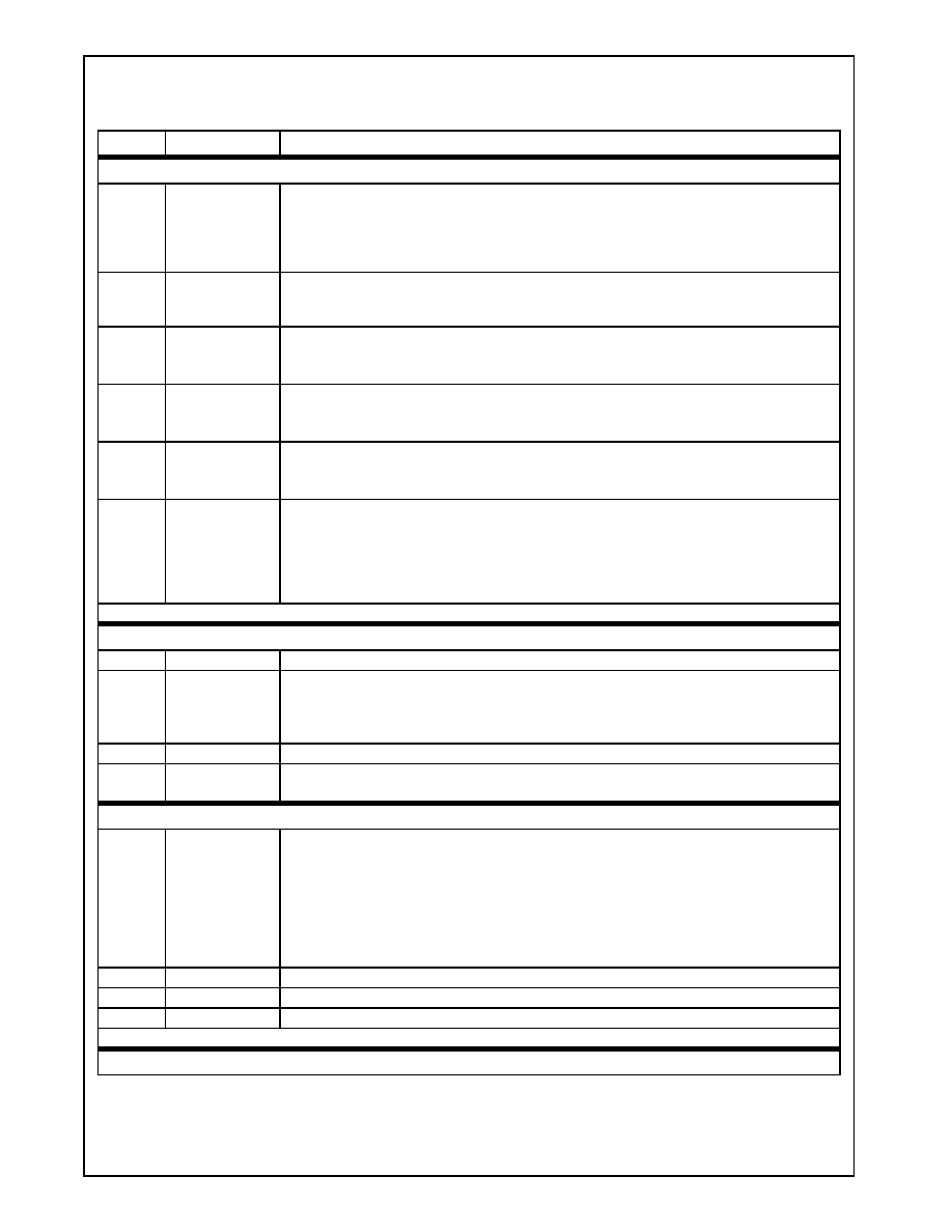
www.national.com
50
Revision 3.1
Processor Programming (
Continued
)
GeodeTM
G
Xm
Pr
ocessor
Index E8h
CCR4 -- Configuration Control Register 4 (R/W)
Default Value = 85h
7
CPUID
Enable CPUID Instruction:
If = 1: The ID bit in the EFLAGS register to be modified and execution of the CPUID instruction
occurs as documented in Table 9-2 on page 202.
If = 0: The ID bit can not be modified and execution of the CPUID instruction causes an invalid
opcode exception.
6
SMI_NEST
SMI Nest:
If = 1: SMI interrupts can occur during SMM mode. SMI handlers can optionally set SMI_NEST high
to allow higher-priority SMI interrupts while handling the current event
5
FPU_FAST_EN
FPU Fast Mode Enable:
If = 0: Disable FPU Fast Mode
If = 1: Enable FPU Fast Mode.
4
DTE_EN
Directory Table Entry Cache:
If = 1: Enables directory table entry to be cached.
Cleared to 0 at reset.
3
MEM_BYP
Memory Read Bypassing:
If = 1: Enables memory read bypassing.
Cleared to 0 at reset.
2:0
IORT(2:0)
I/O Recovery Time: Specifies the minimum number of bus clocks between I/O accesses:
000 = No clock delay
100 = 16-clock delay
001 = 2-clock delay
101 = 32-clock delay (default value after reset)
010 = 4-clock delay
110 = 64-clock delay
011 = 8-clock delay
111 = 128-clock delay
Cleared to 0 at reset.
Note: MAPEN (CCR3[4]) must = 1 to read or write to this register.
Index EBh
CCR7 -- Configuration Control Register 7 (R/W)
Default Value = 00h
7:3
RSVD
Reserved: Set to 0.
2
NMI
Generate NMI:
0 = Do nothing
1 = Generate NMI
In order to generate multiple NMIs, this bit must be set to zero between each setting of 1.
1
RSVD
Reserved: Set to 0.
0
EMMX
Extended MMX Instructions Enable:
If = 1: extended MMX instructions are enabled
Index 20h
PCR -- Performance Control Register (R/W)
Default Value = 07h
7
LSSER
Load/Store Serialize Enable (Reorder Disable): LSSER should be set to ensure that memory-
mapped I/O devices operating outside of the address range 640K to 1M will operate correctly. For
memory accesses above 1 GB, refer to CCR3[7:5] (LSS_34, LSS_23, LSS_12.)
If = 1: All memory read and write operations will occur in execution order (load/store serializing
enabled, reordering disabled).
If = 0: Memory reads and write can be reordered for optimum performance (load/store serializing
disabled, reordering enabled).
Memory accesses in the address range 640K to 1M will always be issued in execution order.
6
RSVD
Reserved: Set to 0.
5
RSVD
Reserved: This is a test bit that must be set to 0.
4:0
RSVD
Reserved: Set to 0.
Note: MAPEN (CCR3[4]) must = 1 to read or write to this register.
Index B0h, B1h, B2h, B3h
SMHR -- SMI Header Address Register (R/W)
Default Value = xxh
Table 3-11. Configuration Registers (Continued)
Bit
Name
Description

Revision 3.1
51
www.national.com
Processor Programming (
Continued
)
GeodeTM
G
Xm
P
r
ocessor
Index
SMHR Bits
SMM Header Address Bits [A31:0]: SMHR address bits [31:0] contain the physical base address
for the SMM header space. For example, bits [31:24] correspond with Index B3h
Refer to Section 3.11.4 "SMM Configuration Registers" on page 80 for more information.
B3h
B2h
B1h
B0h
A[31:24]
A[23:16]
A[15:12]
A[7:0]
Note: MAPEN (CCR3[4]) must = 1 to read or write to this register.
Index CDh, CEh, CFh
SMAR -- SMM Address Region/Size Register (R/W)
Default Value = 00h
Index
SMAR Bits
SMM Address Region Bits [A31:A12]: SMAR address bits [31:12] contain the base address for
the SMM region.
Bits [31:24] correspond with Index CDh
Bits [23:16] correspond with Index CEh
Bits [15:12] correspond with Index CFh[7:4]
Index CFh allows simultaneous access to SMAR address regions bits SMAR[15:12] and size code
bits SIZE[3:0]. During access, the upper 4-bits of Port 23h hold SMAR[15:12].
Refer to Section 3.11.4 "SMM Configuration Registers" on page 80 for more information.
CDh
CEh
CFh[7:4]
A[31:24]
A[23:16]
A[15:12]
CFh[3:0]
SIZE[3:0]
SMM Region Size Bits [3:0]: SIZE bits contain the size code for the SMM region. During access
the lower 4-bits of port 23 hold SIZE[3:0]. Index CFh allows simultaneous access to SMAR address
regions bits SMAR[15:12] (see above) and size code bits.
0000 = SMM Disabled
0100 = 32 KB
1000 = 512 KB
1100 = 8 MB
0001 = 4 KB
0101 = 64 KB
1001 = 1 MB
1101 = 16 MB
0010 = 8 KB
0110 = 128 KB
1010 = 2 MB
1110 = 32 MB
0011 = 16 KB
0111 = 256 KB
1011 = 4 MB
1111 = 4 KB (same as
0001)
Note: SMI_LOCK (CCR3[0]) must = 0, or the CPU must be in SMI mode, to write these registers/bits.
Index FEh
DIR0 -- Device Identification Register 0 (RO)
Default Value = 4xh
7:4
DID[3:0]
Device ID (Read Only): Identifies device as GXm processor.
3:0
MULT[3:0]
Core Multiplier (Read Only) -- Identifies the core multiplier set by the CLKMODE[2:0] pins (see
signal descriptions page 21)
If DIR1 (Index FFh) is 30h-4Fh then MULT[3:0]:
0000 = SYSCLK multiplied by 4 (Test mode only)
0001 = SYSCLK multiplied by 6
0010 = SYSCLK multiplied by 4 (Test mode only)
0011 = SYSCLK multiplied by 6
0100 = SYSCLK multiplied by 7
0101 = SYSCLK multiplied by 8
0110 = SYSCLK multiplied by 7
0111 = SYSCLK multiplied by 5
1xxx = Reserved
If DIR1 (Index FFh) is 50h or greater then MULT[3:0]:
0000 = SYSCLK multiplied by 4 (Test mode only)
0001 = SYSCLK multiplied by 10
0010 = SYSCLK multiplied by 4 (Test mode only)
0011 = SYSCLK multiplied by 6
0100 = SYSCLK multiplied by 9
0101 = SYSCLK multiplied by 5
0110 = SYSCLK multiplied by 7
0111 = SYSCLK multiplied by 8
1xxx = Reserved
Index FFh
DIR1 -- Device Identification Register 1 (RO)
Default Value = xxh
7:0
DIR1
Device Identification Revision (Read Only) -- DIR1 indicates device revision number.
If DIR1 is 30h-33h = GXm processor revision 1.0 - 2.3
If DIR1 is 34h-4Fh = GXm processor revision 2.4 - 3.x
If DIR1 is 50h or greater = GXm processor revision 5.0 - 5.4..
Table 3-11. Configuration Registers (Continued)
Bit
Name
Description
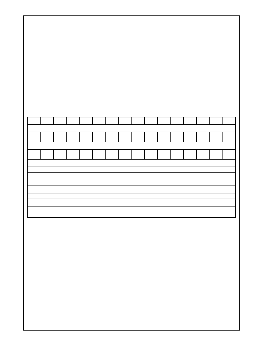
www.national.com
52
Revision 3.1
Processor Programming (
Continued
)
GeodeTM
G
Xm
Pr
ocessor
3.3.2.3
Debug Registers
Six debug registers (DR0-DR3, DR6 and DR7) support
debugging on the GXm processor. Memory addresses
loaded in the debug registers, referred to as "breakpoints,"
generate a debug exception when a memory access of
the specified type occurs to the specified address. A
breakpoint can be specified for a particular kind of mem-
ory access such as a read or write operation. Code and
data breakpoints can also be set allowing debug excep-
tions to occur whenever a given data access (read or write
operation) or code access (execute) occurs. The size of
the debug target can be set to 1, 2, or 4 bytes. The debug
registers are accessed through MOV instructions that can
be executed only at privilege level 0 (real mode is always
privilege level 0).
The Debug Address Registers (DR0-DR3) each contain
the linear address for one of four possible breakpoints.
Each breakpoint is further specified by bits in the Debug
Control Register (DR7). For each breakpoint address in
DR0-DR3, there are corresponding fields L, R/W, and
LEN in DR7 that specify the type of memory access asso-
ciated with the breakpoint.
The R/W field can be used to specify instruction execution
as well as data access breakpoints. Instruction execution
breakpoints are always taken before execution of the
instruction that matches the breakpoint. The Debug Reg-
isters are mapped in Table 3-12
Table 3-12. Debug Registers
31 30 29 28 27 26 25 24 23 22 21 20 19 18 17 16 15 14 13 12 11 10
9
8
7
6
5
4
3
2
1
0
DR7 Register
Debug Control Register 7 (R/W)
LEN3
R/W3
LEN2
R/W2
LEN1
R/W1
LEN0
R/W0
0
0
G
D
0
0
1
0
0
G
3
L
3
G
2
L
2
G
1
L
1
G
0
L0
DR6 Register
Debug Status Register 6 (RO)
0
0
0
0
0
0
0
0
0
0
0
0
0
0
0
0
B
T
B
S
0
1
1
1
1
1
1
1
1
1
B3 B2 B1 B0
DR3 Register`
Debug Address Register 3 (R/W))
Breakpoint 3 Linear Address
DR2 Register
Debug Address Register 2 (R/W)
Breakpoint 2 Linear Address
DR1 Register
Debug Address Register 1 (R/W)
Breakpoint 1 Linear Address
DR0 Register
Debug Address Register 0 (R/W)
Breakpoint 0 Linear Address
Note: All bits marked as 0 or 1 are reserved and should not be modified.
Revision 3.1
53
www.national.com
Processor Programming (
Continued
)
GeodeTM
G
Xm
P
r
ocessor
The Debug Status Register (DR6) reflects conditions that
were in effect at the time the debug exception occurred.
The contents of the DR6 register are not automatically
cleared by the processor after a debug exception occurs,
and therefore should be cleared by software at the appro-
priate time. Table 3-13 lists the field definitions for the DR6
and DR7 registers.
Code execution breakpoints may also be generated by
placing the breakpoint instruction (INT3) at the location
where control is to be regained. The single-step feature
may be enabled by setting the TF flag (bit 8) in the
EFLAGS register. This causes the processor to perform a
debug exception after the execution of every instruction.
Debug Registers 6 and 7 are shown in Table 3-13.
Table 3-13. DR7 and DR6 Bit Definitions
Field(s)
Number
of Bits
Description
DR7 Register
Debug Control Register 7 (R/W)
R/Wn
2
Applies to the DRn breakpoint address register:
00 = Break on instruction execution only
01 = Break on data write operations only
10 = Not used
11 = Break on data reads or write operations.
LENn
2
Applies to the DRn breakpoint address register:
00 = One-byte length
01 = Two-byte length
10 = Not used
11 = Four-byte length.
Gn
1
If = 1: breakpoint in DRn is globally enabled for all tasks and is not cleared by the processor as the
result of a task switch.
Ln
1
If = 1: breakpoint in DRn is locally enabled for the current task and is cleared by the processor as the
result of a task switch.
GD
1
Global disable of debug register access. GD bit is cleared whenever a debug exception occurs.
DR6 Register
Debug Status Register 6 (RO)
Bn
1
Bn is set by the processor if the conditions described by DRn, R/Wn, and LENn occurred when the
debug exception occurred, even if the breakpoint is not enabled via the Gn or Ln bits.
BT
1
BT is set by the processor before entering the debug handler if a task switch has occurred to a task with
the T bit in the TSS set.
BS
1
BS is set by the processor if the debug exception was triggered by the single-step execution mode (TF
flag, bit 8, in EFLAGS set).
Note: n = 0, 1, 2, and 3
www.national.com
54
Revision 3.1
Processor Programming (
Continued
)
GeodeTM
G
Xm
Pr
ocessor
3.3.2.4
Test Registers
The five test registers are used in testing the processor's
Translation Lookaside Buffer (TLB) and on-chip cache. TR6
and TR7 are used for TLB testing, and TR3-TR5 are used
for cache testing. Table 3-14 is a register map for the Test
Registers with their bit definitions given in Tables 3-15 and
3-17.
TLB Test Registers
The processor's TLB is a 32-entry, four-way set associa-
tive memory. Each TLB entry consists of a 24-bit tag and
20-bit data. The 24-bit tag represents the high-order 20
bits of the linear address, a valid bit, and three attribute
bits. The 20-bit data portion represents the upper 20 bits
of the physical address that corresponds to the linear
address.
The TLB Test Data Register (TR7) contains the upper 20
bits of the physical address (TLB data field), three LRU
bits and a control bit. During TLB write operations, the
physical address in TR7 is written into the TLB entry
selected by the contents of TR6. During TLB lookup oper-
ations, the TLB data selected by the contents of TR6 is
loaded into TR7. Table 3-15 lists the bit definitions for TR7
and TR6.
The TLB Test Control Register (TR6) contains a com-
mand bit, the upper 20 bits of a linear address, a valid bit
and the attribute bits used in the test operation. The con-
tents of TR6 are used to create the 24-bit TLB tag during
both write and read (TLB lookup) test operations. The
command bit defines whether the test operation is a read
or a write.
Table 3-14. TLB Test Registers
31 30 29 28 27 26 25 24 23 22 21 20 19 18 17 16 15 14 13 12 11 10
9
8
7
6
5
4
3
2
1
0
TR7 Register
TLB Test Data Register (R/W)
Physical Address
0
0
TLB LRU
0
0
PL
REP
0
0
TR6 Register
TLB Test Control Register (R/W)
Linear Address
V
D D# U U# R R#
0
0
0
0
C

Revision 3.1
55
www.national.com
Processor Programming (
Continued
)
GeodeTM
G
Xm
P
r
ocessor
Table 3-15. TR7-TR6 Bit Definitions
Bit
Name
Description
TR7 Register
TLB Test Data Register (R/W)
31:12
Physical
Address
Physical Address:
TLB lookup: Data field from the TLB.
TLB write: Data field written into the TLB.
11:10
RSVD
Reserved: Set to 0.
9:7
TLB LRU
LRU Bits:
TLB lookup: LRU bits associated with the TLB entry before the TLB lookup.
TLB write: Ignored.
4
PL
PL Bit:
TLB lookup: If PL = 1, read hit occurred. If PL = 0, read miss occurred.
TLB write: If PL = 1, REP field is used to select the set. If PL = 0, the pseudo-LRU replacement algorithm
is used to select the set.
3:2
REP
Set Selection:
TLB lookup: If PL = 1, this field indicates the set in which the tag was found. If PL = 0, undefined data.
TLB write: If PL = 1, this field selects one of the four sets for replacement. If PL = 0, ignored.
1:0
RSVD
Reserved: Set to 0.
TR6 Register
TLB Test Control Register (R/W)
31:12
Linear
Address
Linear Address:
TLB lookup: The TLB is interrogated per this address. If one and only one match occurs in the TLB, the
rest of the fields in TR6 and TR7 are updated per the matching TLB entry.
TLB write: A TLB entry is allocated to this linear address.
11
V
Valid Bit:
TLB write: If V = 1, the TLB entry contains valid data. If V = 0, target entry is invalidated.
10:9
8:7
6:5
D, D#
U, U#
R, R#
Dirty Attribute Bit and its Complement (D, D#)
User/Supervisor Attribute Bit and its Complement (U, U#)
Read/Write Attribute Bit and its Complement (R, R#)
Effect on TLB Lookup
Effect on TLB Write
00 =
Do not match
Undefined
01 =
Match if D, U, or R bit is a 0
Clear the bit
10 =
Match if D, U, or R bit is a 1
Set the bit
11 =
Match if D, U, or R bit is either a 1 or 0
Undefined
4:1
RSVD
Reserved: Set to 0.
0
C
Command Bit:
If C = 1: TLB lookup.
If C = 0: TLB write.
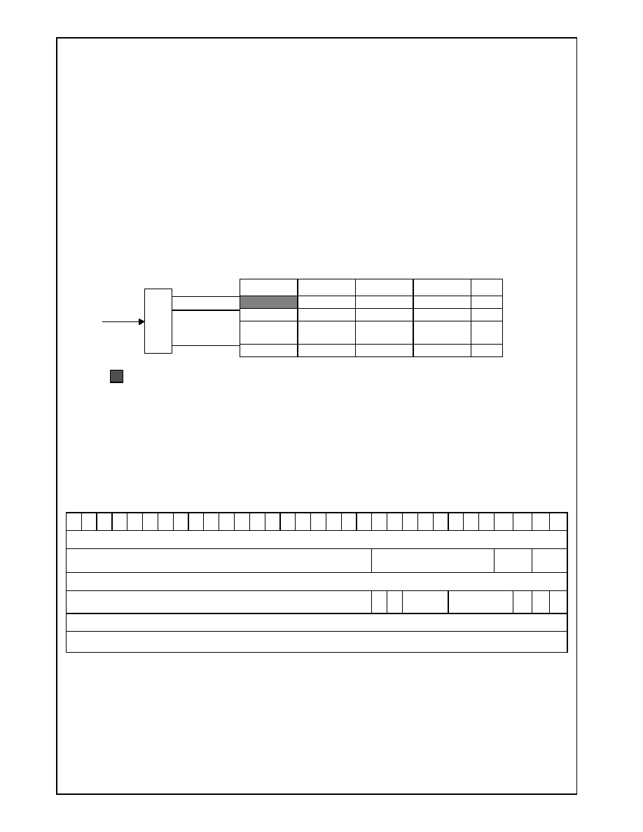
www.national.com
56
Revision 3.1
Processor Programming (
Continued
)
GeodeTM
G
Xm
Pr
ocessor
Cache Test Registers
The processor's 16 KB on-chip cache is a four-way set
associative memory that is configured as write-back
cache. Each cache set contains 256 entries. Each entry
consists of a 20-bit tag address, a 16-byte data field, a
valid bit, and four dirty bits.
The 20-bit tag represents the high-order 20 bits of the
physical address. The 16-byte data represents the 16
bytes of data currently in memory at the physical address
represented by the tag. The valid bit indicates whether the
data bytes in the cache actually contain valid data. The
four dirty bits indicate if the data bytes in the cache have
been modified internally without updating external mem-
ory (write-back configuration). Each dirty bit indicates the
status for one double-word (4 bytes) within the 16-byte
data field.
For each line in the cache, there are three LRU bits that
indicate which of the four sets was most recently
accessed. A line is selected using bits [11:4] of the physi-
cal address. Figure 3-1 illustrates the CPU cache archi-
tecture.
The CPU contains three test registers (TR5-TR3) that
allow testing of its internal cache. Bit definitions for the
cache test registers are shown in Table 3-17. Using a 16-
byte cache fill buffer and a 16-byte cache flush buffer,
cache reads and writes may be performed.
.
Figure 3-1. CPU Cache Architecture
D
E
C
O
D
E
255
254
.
.
0
A11-A4
Line
Address
= Cache Entry (153 bits)
Tag Address (20 bits)
Data (128 bits)
Valid Status (1 bit)
Dirty Status (4 bits)
Set 0
Set 1
Set 2
Set 3
LRU
.
.
.
.
.
.
.
.
.
.
152 --- 0
152 --- 0
152 --- 0
152 --- 0
2 --- 0
Table 3-16. Cache Test Registers
31 30 29 28 27 26 25 24 23 22 21 20 19 18 17 16 15 14 13 12 11 10
9
8
7
6
5
4
3
2
1
0
TR5 Register (R/W)
RSVD
Line Selection
Set/
DWORD
Control
Bits
TR4 Register (R/W)
Cache Tag Address
0
V
a
lid
LRU Bits
Dirty Bits
0
0
0
TR3 Register (R/W)
Cache Data

Revision 3.1
57
www.national.com
Processor Programming (
Continued
)
GeodeTM
G
Xm
P
r
ocessor
Table 3-17. TR5-TR3 Bit Definitions
Bit
Name
Description
TR5 Register (R/W)
11:4
Line Selection
Line Selection:
Physical address bits 11-4 used to select one of 256 lines.
3:2
Set/DWORD
Set/DWord Selection:
Cache read: Selects which of the four sets in the cache is used as the source for data
transferred to the cache flush buffer.
Cache write: Selects which of the four sets in the cache is used as the destination for data transferred
from the cache fill buffer.
Flush buffer read: Selects which of the four Dword in the flush buffer is
used during a TR3 read.
Fill buffer write: Selects which of the four Dword in the fill buffer is written during a TR3 write.
1:0
Control Bits
Control Bits:
If = 00: flush read or fill buffer write.
If = 01: cache write.
If = 10: cache read.
If = 11: cache flush.
TR4 Register (R/W)
31:12
Upper Tag
Address
Upper Tag Address:
Cache read: Upper 20 bits of tag address of the selected entry.
Cache write: Data written into the upper 20 bits of the tag address of the selected entry.
10
Valid Bit
Valid Bit:
Cache read: Valid bit for the selected entry.
Cache write: Data written into the valid bit for the selected entry.
9:7
LRU Bits
LRU Bits:
Cache read: The LRU bits for the selected line.
xx1 = Set 0 or Set 1 most recently accessed.
xx0 = Set 2 or Set 3 most recently accessed.
x1x = Most recent access to Set 0 or Set 1 was to Set 0.
x0x = Most recent access to Set 0 or Set 1 was to Set 1.
1xx = Most recent access to Set 2 or Set 3 was to Set 2.
0xx = Most recent access to Set 2 or Set 3 was to Set 3.
Cache write: Ignored.
6:3
Dirty Bits
Dirty Bits:
Cache read: The dirty bits for the selected entry (one bit per DWord).
Cache write: Data written into the dirty bits for the selected entry.
2:0
RSVD
Reserved: Set to 0.
TR3 Register (R/W)
31:0
Cache Data
Cache Data:
Flush buffer read: Data accessed from the cache flush buffer.
Fill buffer write: Data to be written into the cache fill buffer.
www.national.com
58
Revision 3.1
Processor Programming (
Continued
)
GeodeTM
G
Xm
Pr
ocessor
There are five types of test operations that can be exe-
cuted:
∑ Flush buffer read
∑ Fill buffer write
∑ Cache write
∑ Cache read
∑ Cache flush
These operations are described in detail in Table 3-18. To
fill a cache line with data, the fill buffer must be written four
times. Once the fill buffer holds a complete cache line of
data (16 bytes), a cache write operation transfers the data
from the fill buffer to the cache.
To read the contents of a cache line, a cache read opera-
tion transfers the data in the selected cache line to the
flush buffer. Once the flush buffer is loaded, the program-
mer accesses the contents of the flush buffer by executing
four flush buffer read operations.
Table 3-18. Cache Test Operations
Test Operation
Code Sequence
Action Taken
Flush Buffer Read
MOV TR5, 0h
MOV dest,TR3
Set DWORD = 0, control = 00 = flush buffer read.
Flush buffer (31:0) --> dest.
MOV TR5, 4h
MOV dest,TR3
Set DWORD = 1, control = 00 = flush buffer read.
Flush buffer (63:32) --> dest.
MOV TR5, 8h
MOV dest,TR3
Set DWORD = 2, control = 00 = flush buffer read.
Flush buffer (95:64) --> dest.
MOV TR5, Ch
MOV dest,TR3
Set DWORD = 3, control = 00 = flush buffer read.
Flush buffer (127:96) --> dest.
Fill Buffer Write
MOV TR5, 0h
MOV TR3, cache_data
Set DWORD = 0, control = 00 = fill buffer write.
Cache_data --> fill buffer (31:0).
MOV TR5, 4h
MOV TR3, cache_data
Set DWORD = 1, control = 00 = fill buffer write.
Cache_data --> fill buffer (63:32).
MOV TR5, 8h
MOV TR3, cache_data
Set DWORD = 2, control = 00 = fill buffer write.
Cache_data --> fill buffer (95:64).
MOV TR5, Ch
MOV TR3, cache_data
Set DWORD = 3, control = 00 = fill buffer write.
Cache_data --> fill buffer (127:96).
Cache Write
MOV TR4, cache_tag
Cache_tag --> tag address, valid and dirty bits.
MOV TR5, line+set+control=01
Fill buffer (127:0) --> cache line (127:0).
Cache Read
MOV TR5, line+set+control=10
MOV dest, TR4
Cache line (127:0) --> flush buffer (127:0).
Cache line tag address, valid/LRU/dirty bits --> dest.
Cache Flush
MOV TR5, 3h
Control = 11 = cache flush, all cache valid bits = 0.

Revision 3.1
59
www.national.com
Processor Programming (
Continued
)
GeodeTM
G
Xm
P
r
ocessor
3.3.3
Model Specific Register Set
The Model Specific Register (MSR) Set is used to monitor
the performance of the processor or a specific component
within the processor.
A MSR can be read using the RDMSR instruction, opcode
0F32h. During a MSR read, the contents of the particular
MSR, specified by the ECX Register, is loaded into the
EDX:EAX Registers.
A MSR can be written using the WRMSR instruction,
opcode 0F30h. During a MSR write, the contents of
EX:EAX are loaded into the MSR specified in the ECX
Register.
The RDMSR and WRMSR instructions are privileged
instructions.
The GXm processor contains one 64-bit Model Specific
Register (MSR10) the Time Stamp Counter (TSC).
3.3.4
Time Stamp Counter
The processor contains a model specific register (MSR)
called the Time Stamp Counter (TSC). The TSC,
(MSR[10]), is a 64-bit counter that counts the internal
CPU clock cycles since the last reset. The TSC uses a
continuous CPU core clock and will continue to count
clock cycles even when the processor is in suspend or
shutdown mode.
The TSC is read using a RDMSR instruction, opcode 0F
32h, with the ECX register set to 10h. During a TSC read,
the contents of the TSC is loaded into the EDX:EAX regis-
ters.
The TSC is written to using a WRMSR instruction, opcode
0F 30h with the ECX register set to 10h. During a TSC
write, the contents of EX:EAX are loaded into the TSC.
The RDMSR and WRMSR instructions are privileged
instructions.
In addition, the TSC can be read using the RDTSC
instruction, opcode 0F 31h. The RDTSC instruction loads
the contents of the TSC into EDX:EAX. The use of the
RDTSC instruction is restricted by the TSC flag (bit 2) in
the CR4 register (refer to Tables 3-6 and 3-7 on pages 45
and 45 for CR4 register information). When the TSC bit =
0, the RDTSC instruction can be executed at any privilege
level. When the TSC bit = 1, the RDTSC instruction can
only be executed at privilege level 0.
www.national.com
60
Revision 3.1
Processor Programming (
Continued
)
GeodeTM
G
Xm
Pr
ocessor
3.4
ADDRESS SPACES
The GXm processor can directly address either memory
or I/O space. Figure 3-2 illustrates the range of addresses
available for memory address space and I/O address
space. For the CPU, the addresses for physical memory
range between 0000 0000h and FFFFFFFFh (4 GBytes).
The accessible I/O addresses space ranges between
00000000h and 0000 FFFFh (64 KB). The CPU does not
use coprocessor communication space in upper I/O space
between 800000F8h and 8000 00FFh as do the 386-style
CPUs. The I/O locations 22h and 23h are used for GXm
processor configuration register access.
3.4.1
I/O Address Space
The CPU I/O address space is accessed using IN and
OUT instructions to addresses referred to as "ports." The
accessible I/O address space is 64 KB and can be
accessed as 8-bit, 16-bit or 32-bit ports.
The GXm processor configuration registers reside within
the I/O address space at port addresses 22h and 23h and
are accessed using the standard IN and OUT instructions.
The configuration registers are modified by writing the
index of the configuration register to port 22h, and then
transferring the data through port 23h. Accesses to the
on-chip configuration registers do not generate external
I/O cycles. However, each operation on port 23h must be
preceded by a write to port 22h with a valid index value.
Otherwise, subsequent port 23h operations will communi-
cate through the I/O port to produce external I/O cycles with-
out modifying the on-chip configuration registers. Write
operations to port 22h outside of the CPU index range
(C0h-CFh and FEh-FFh) result in external I/O cycles and
do not affect the on-chip configuration registers. Reading
port 22h generates external I/O cycles.
I/O accesses to port address range 3B0h through 3DFh
can be trapped to SMI by the CPU if this option is enabled
in the BC_XMAP_1 register (see SMIB, SMIC, and SMID
bits in Table 4-10 on page 101). Figure 3-2 illustrates the
I/O address space.
3.4.2
Memory Address Space
The processor directly addresses up to 4 GB of physical
memory even though the memory controller addresses
only 1 GB of DRAM. Memory address space is accessed
as bytes, words (16 bits) or DWORDs (32 bits). Words
and DWORDs are stored in consecutive memory bytes
with the low-order byte located in the lowest address. The
physical address of a word or DWORD is the byte address
of the low-order byte.
The processor allows memory to be addressed using nine
different addressing modes. These addressing modes are
used to calculate an offset address, often referred to as an
effective address. Depending on the operating mode of
the CPU, the offset is then combined, using memory man-
agement mechanisms, into a physical address that is
applied to the physical memory devices.
Memory management mechanisms consist of segmenta-
tion and paging. Segmentation allows each program to
use several independent, protected address spaces. Pag-
ing translates a logical address into a physical address
using translation lookup tables. Virtual memory is often
implemented using paging. Either or both of these mecha-
nisms can be used for management of the GXm proces-
sor memory address space.
Figure 3-2. Memory and I/O Address Spaces
Physical
Memory Space
Accessible
Programmed
I/O Space
FFFFFFFFh
0000FFFFh
00000000h
FFFFFFFFh
00000000h
Physical Memory
4 GB
Not
Accessible
64 KB
CPU General
Configuration
Register I/O
Space
00000023h
00000022h

Revision 3.1
61
www.national.com
Processor Programming (
Continued
)
GeodeTM
G
Xm
P
r
ocessor
3.5
OFFSET, SEGMENT, AND PAGING MECHANISMS
The mapping of address space into a sequence of mem-
ory locations (often cached) is performed by the offset,
segment and paging mechanisms.
In general, the offset, segment and paging mechanisms
work in tandem as shown below:
instruction offset
offset mechanism
offset address
offset address
segment mechanism
linear address
linear address
paging mechanism
physical page.
As will be explained, the actual operations depend on sev-
eral factors such as the current operating mode and if
paging is enabled. Note: the paging mechanism uses part
of the linear address as an offset on the physical page.
3.6
OFFSET MECHANISM
In all operating modes, the offset mechanism computes
an offset (effective) address by adding together up to
three values: a base, an index and a displacement. The
base, if present, is the value in one of eight general regis-
ters at the time of the execution of the instruction. The
index, like the base, is a value that is contained in one of
the general registers (except the ESP register) when the
instruction is executed. The index differs from the base in
that the index is first multiplied by a scale factor of 1, 2, 4
or 8 before the summation is made. The third component
added to the memory address calculation is the displace-
ment that is a value supplied as part of the instruction.
Figure 3-3 illustrates the calculation of the offset address.
Nine valid combinations of the base, index, scale factor
and displacement can be used with the CPU instruction
set. These combinations are listed in Table 3-19 on page
61. The base and index both refer to contents of a register
as indicated by [Base] and [Index].
In real mode operation, the CPU only addresses the low-
est 1 MB of memory and the offset contains 16-bits. In
protective mode the offset contains 32 bits. Initialization
and transition to protective mode is described in Section
3.13.4 "Initialization and Transition to Protected Mode" on
page 87.
Figure 3-3. Offset Address Calculation
Table 3-19. Memory Addressing Modes
Index
Base
Displacement
Scaling
x1, x2, x4, x8
Offset Address
(Effective Address)
+
Addressing Mode
Base
Index
Scale
Factor
(SF)
Displacement
(DP)
Offset Address (OA)
Calculation
Direct
x
OA = DP
Register Indirect
x
OA = [BASE]
Based
x
x
OA = [BASE] + DP
Index
x
x
OA = [INDEX] + DP
Scaled Index
x
x
x
OA = ([INDEX] * SF) + DP
Based Index
x
x
OA = [BASE] + [INDEX]
Based Scaled Index
x
x
x
OA = [BASE] + ([INDEX] * SF)
Based Index with
Displacement
x
x
x
OA = [BASE] + [INDEX] + DP
Based Scaled Index with
Displacement
x
x
x
x
OA = [BASE] + ([INDEX] * SF) + DP

www.national.com
62
Revision 3.1
Processor Programming (
Continued
)
GeodeTM
G
Xm
Pr
ocessor
3.7
DESCRIPTORS AND SEGMENT MECHANISMS
Memory is divided into contiguous regions called "seg-
ments." The segments allow the partitioning of individual
elements of a program. Each segment provides a zero
address-based private memory for such elements as
code, data and stack space.
The segment mechanisms select a segment in memory.
Memory is divided into an arbitrary number of segments,
each containing usually much less than the 2
32
byte (4
GByte) maximum.
There are two segment mechanisms, one for Real and
Virtual 8086 Operating Modes, and one for Protective
Mode.
3.7.1
Real and Virtual 8086 Mode Segment
Mechanisms
Real Mode Segment Mechanism
In real mode operation, the CPU addresses only the low-
est 1 MB of memory. In this mode a selector located in
one of the segment registers is used to locate a segment.
To calculate a physical memory address, the 16-bit seg-
ment base address located in the selected segment regis-
ter is multiplied by 16 and then a 16-bit offset address is
added. The resulting 20-bit address is then extended with
twelve zeros in the upper address bits to crate 32-bit phys-
ical address.
The value of the selector (the INDEX field) is multiplied by
16 to produce a base address (Figure 3-4.) The base
address is summed with the instruction offset value to pro-
duce a physical address.
Virtual 8086 Mode Segment Mechanism
In Virtual 8086 mode the operation is performed as in real
mode except that a paging mechanism is added. When
paging is enabled, the paging mechanism translates the
linear address into a physical address using cached look-
up tables (refer to Section 3.9 "Paging Mechanism" on
page 72).
Figure 3-4. Real Mode Address Calculation
Offset Mechanism
Selected Segment
Register
Offset Address
000h
X 16
16
12
20
20
16
32
Linear Address
(Physical Address)
Base Address
12 High Order Address Bits
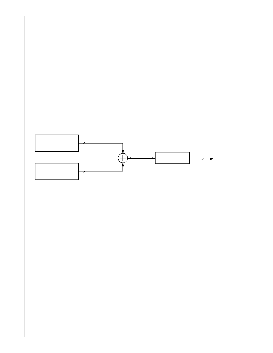
Revision 3.1
63
www.national.com
Processor Programming (
Continued
)
GeodeTM
G
Xm
P
r
ocessor
3.7.2
Segment Mechanism in Protective Mode
The segment mechanism in protective mode is more com-
plex. Basically as in Real and Virtual 8086 modes the off-
set address is added to the segment base address to
produce a linear address (Figure 3-5). However, the cal-
culation of the segment base address is based on the
contents of descriptor tables.
Again, if paging is enabled the linear address is further
processed by the paging mechanism.
A more detailed look at the segment mechanisms for real,
virtual 8086 and protective modes is illustrated in Figure
3-6. In protective mode, the segment selector is cached.
This is illustrated in Figure 3-7 on page 65.
3.7.2.1
Segment Selectors
The segment registers are used to store segment selec-
tors. In protective mode, the segment selectors are
divided in to three fields: the RPL, TI and INDEX fields as
shown in Figure 3-6.
The segments are assigned permission levels to prevent
application program errors from disrupting operating pro-
grams. The Requested Privilege Level (RPL) determines
the Effective Privilege Level of an instruction. RPL = 0 indi-
cates the most privileged level, and RPL = 3 indicates the
least privileged level. Refer to Section 3.13 "Protection" on
page 86.
Descriptor tables hold descriptors that allow management
of segments and tables in address space while in protec-
tive mode. The Table Indicator Bit (TI) in the selector
selects either the General Descriptor Table (GDT) or one
Local Descriptor Tables (LDT) tables. If TI = 0, GDT is
selected; if TI =1, LDT is selected. The 13-bit INDEX field
in the segment selector is used to index a GDT or LDT
table.
Figure 3-5. Protected Mode Address Calculation
Offset Mechanism
Selector Mechanism
Offset Address
32
32
32
32
Optional
Physical
Segment Base
Address
Address
Paging Mechanism
Linear
Address
Memory
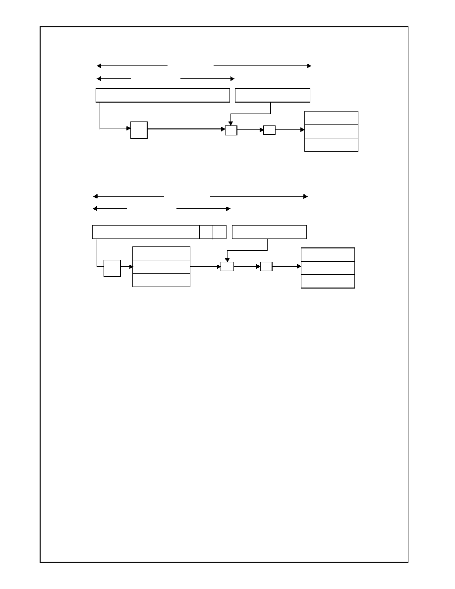
www.national.com
64
Revision 3.1
Processor Programming (
Continued
)
GeodeTM
G
Xm
Pr
ocessor
Figure 3-6. Selector Mechanisms
15
3
2 1
0
INDEX
TI
INSTRUCTION OFFSET
Segment Selector
Segment Descriptor
Base
GDT or LDT Descriptor Table
Main Memory
Segment
p
p = Paging Mechanism
RPL
+
Linear
Address
Address
Physical
Address
15
0
INDEX
INSTRUCTION OFFSET
Logical Address
Base
Main Memory
Segment
p
+
Linear
Address
Address
Physical
Address
x 16
p= Paging Mechanism for Virtual 8086 Mode only
Real and Virtual 8086 Modes
Address
Logical
Segment Selector
Protective Mode
Logical Address
x 8
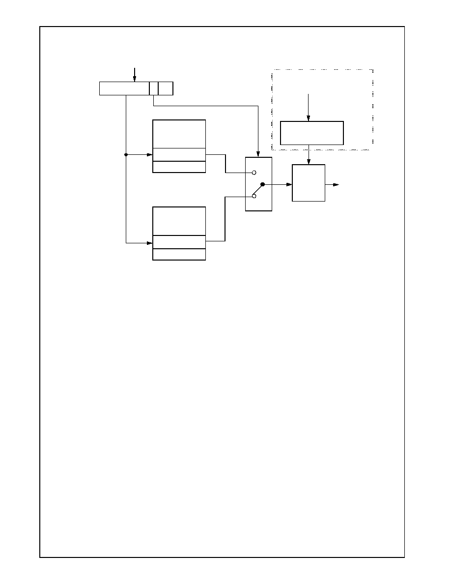
Revision 3.1
65
www.national.com
Processor Programming (
Continued
)
GeodeTM
G
Xm
P
r
ocessor
Figure 3-7. Selector Mechanism Caching
INDEX
TI RPL
Selector Load Instruction
15
0
Selector
In Segment
Register
Segment
Descriptor
Segment
Descriptor
Global Descriptor
Table
Local Descriptor
Table
TI = 0
TI = 1
Cached Segment
Segment
Segment
Segment Register
Selected By Decoded
Instruction
Caching
Cached
and Descriptor
Selector
Used If
Available
Base
Address

www.national.com
66
Revision 3.1
Processor Programming (
Continued
)
GeodeTM
G
Xm
Pr
ocessor
3.7.3
GDTR and LDTR Registers
The GDT, and LDT descriptor tables are defined by the
Global Descriptor Table Register (GDTR) and the Local
Descriptor Table Register (LDTR) respectively. Some texts
refer to these registers as GDT, and LDT descriptors.
The following instructions are used in conjunction with the
GDT and LDT registers:
∑ LGDT - Load memory to GDTR
∑ LLDT - Load memory to LDTR
∑ SGDT - Store GDTR to memory
∑ SLDT - Store LDTR to memory
The GDTR is set up in REAL mode using the LGDT
instruction. This is possible as the LGDT instruction is one
of two instructions that directly load a linear address
(instead of a segment relative address) in protective
mode. (The other instruction is the Load Interrupt Descrip-
tor Table [LIDT]).
As shown in Table 3-20, the GDT registers contain a
BASE ADDRESS field and a LIMIT field that define the
GDT tables. (The IDTR is described in Section 3.7.3.2
"Task, Gate and Interrupt Descriptors" on page 67.)
Also shown in Table 3-20, the LDTR is only two bytes wide
as it contains only a SELECTOR field. The contents of the
SELECTOR field point to a descriptor in the GDT.
3.7.3.1
Segment Descriptors
There are several types of descriptors. A segment
descriptor defines the base address, limit and attributes of
a memory segment.
The GDT or LDT can hold several types of descriptors. In
particular, the segment descriptors are stored in either of
two registers, the GDT, or the LDT as shown in Table 3-
20). Either of these tables can store as many as 8,192
(2
13
) eight-byte selectors taking as much as 64 KB of
memory.
The first descriptor in the GDT (location 0) is not used by
the CPU and is referred to as the "null descriptor."
Types of Segment Descriptors
The type of memory segments are defined by correspond-
ing types of segment descriptors:
∑ Code Segment Descriptors
∑ Data Segment Descriptors
∑ Stack Segment Descriptors
∑ LDT Segment Descriptors
Table 3-20. GDTR, LDTR and IDTR Registers
47
16 15 14 13 12 11 10
9
8
7
6
5
4
3
2
1
0
GDT Register
Global Descriptor Table Register
BASE
LIMIT
IDT Register
Interrupt Descriptor Table Register
BASE
LIMIT
LDT Register
Local Descriptor Table Register
SELECTOR
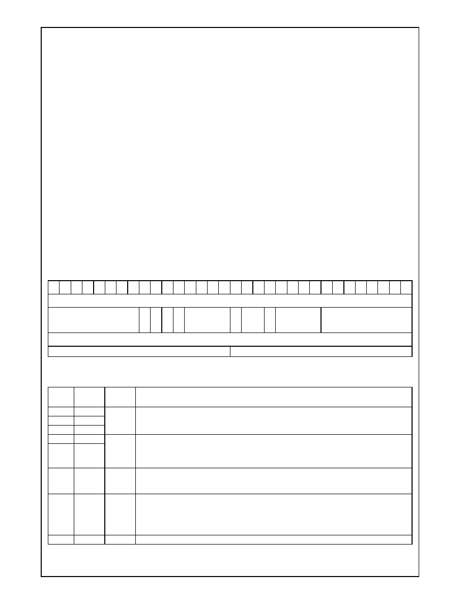
Revision 3.1
67
www.national.com
Processor Programming (
Continued
)
GeodeTM
G
Xm
P
r
ocessor
3.7.3.2
Task, Gate and Interrupt Descriptors
Besides segment descriptors there are descriptors used
in task switching, switching between tasks with different
priority and those used to control interrupt functions:
∑ Task State Segment Table Descriptors
∑ Gate Table Descriptors
∑ Interrupt Descriptors.
All descriptors have some things in common. They are all
eight bytes in length and have three fields (BASE, LIMIT
and TYPE). The BASE field defines the starting location
for the table or segment. The LIMIT field defines the size
and the TYPE field depends on the type of descriptor.
One of the main functions of the TYPE field is to define
the access rights to the associated segment or table.
Interrupt Descriptor Table
The Interrupt Descriptor Table is an array of 256 8-byte (4-
byte for real mode) interrupt descriptors, each of which is
used to point to an interrupt service routine. Every inter-
rupt that may occur in the system must have an associ-
ated entry in the IDT. The contents of the IDTR are
completely visible to the programmer through the use of
the SIDT instruction.
The IDT descriptor table is defined by the Interrupt
Descriptor Table Register (IDTR). Some texts refer to this
register as an IDT descriptor.
The following instructions are used in conjunction with the
IDTR registers:
∑ LIDT - Load memory to IDTR
∑ SIDT - Store IDTR to memory
The IDTR is set up in REAL mode using the LIDT instruc-
tion. This is possible as the LIDT instructions is only one
of two instructions that directly load a linear address
(instead of a segment relative address) in protective
mode.
As previously shown in Table 3-20, the IDTR contains a
BASE ADDRESS field and a LIMIT field that define the
IDT tables.
3.7.4
Descriptor Bit Structure
The bit structure for application and system descriptors is
shown in Table 3-21. The explanation of the TYPE field is
shown in Table 3-23 on page 68.
Table 3-21. Application and System Segment Descriptors
31 31 29 28 27 26 25 24 23 22 21 20 19 18 17 16 15 14 13 12 11 10
9
8
7
6
5
4
3
2
1
0
Memory Offset +4
BASE[31:24]
G
D
0
A
V
L
LIMIT[19:16]
P
DPL
S
TYPE
BASE[23:16]
Memory Offset +0
BASE[15:0]
LIMIT[15:0]
Table 3-22. Application and System Segment Descriptors Bit Definitions
Bit
Memory
Offset
Name
Description
31:24
+4
BASE
Segment Base Address: Three fields which collectively define the base location for the segment in
4 GB physical address space.
7:0
+4
31:16
+0
19:16
+4
LIMIT
Segment Limit: Two fields that define the size of the segment based on the Segment Limit
Granularity Bit.
If G = 1: Limit value interpreted in units of 4 KB.
If G = 0: Limit value is interpreted in bytes.
15:0
+0
23
+4
G
Segment Limit Granularity Bit: Defines LIMIT multiplier.
If G = 1: Limit value interpreted in units of 4 KB. Segment size ranges from 1 byte to 1 MB.
If G = 0: Limit value is interpreted in bytes. Segment size ranges from 4 KB to 4 GB.
22
+4
D
Default Length for Operands and Effective Addresses:
If D = 1: Code segment = 32-bit length for operands and effective addresses
If D = 0: Code segment = 16-bit length for operands and effective addresses
If D = 1: Data segment = Pushes, calls and pop instructions use 32-bit ESP register
If D = 0: Data segment = Stack operations use 16-bit SP register
20
+4
AVL
Segment Available: This field is available for use by system software.
www.national.com
68
Revision 3.1
Processor Programming (
Continued
)
GeodeTM
G
Xm
Pr
ocessor
15
+4
P
Segment Present:
If = 1: Segment is memory segment allocated.
If = 0: The BASE and LIMIT fields become available for use by the system. Also, If = 0, a segment-
not-present exception generated when selector for the descriptor is loaded into a segment register
allowing virtual memory management.
14:13
+4
DPL
Descriptor Privilege Level:
If = 00: Highest privilege level
If = 11: Low privilege level
12
+4
S
Descriptor Type:
If = 1: Code or data segment
If = 0: System segment
11:8
+4
TYPE
Segment Type: Refer to Table 3-23 on page 68 for TYPE bit definitions.
Bit 11 = Executable
Bit 10 = Conforming if bit 12 = 1
Bit 10 = Expand Down if bit 12 = 0
Bit 9 = Readable, if Bit 12 = 1
Bit 9 = Writable, if Bit 12 = 0
Bit 8 = Accessed
Table 3-22. Application and System Segment Descriptors Bit Definitions (Continued)
Bit
Memory
Offset
Name
Description
Table 3-23. Application and System Segment Descriptors TYPE Bit Definitions
TYPE
Bits [11:8]
System Segment and Gate Types
Bit 12 = 0
Application Segment Types
Bit 12 = 1
Num
SEWA
TYPE (Data Segments)
0
0000
Reserved
Data
Read-Only
1
0001
Available 16-Bit TSS
Data
Read-Only, accessed
2
0010
LDT
Data
Read/Write
3
0011
Busy 16-Bit TSS
Data
Read/Write accessed
4
0100
16-Bit Call Gate
Data
Read-Only, expand down
5
0101
Task Gate
Data
Read-Only, expand down, accessed
6
0110
16-Bit Interrupt Gate
Data
Read/Write, expand down
7
0111
16-Bit Trap Gate
Data
Read/Write, expand down, accessed
Num
SCRA
TYPE (Code Segments)
8
1000
Reserved
Code
Execute-Only
9
1001
Available 32-Bit TSS
Code
Execute-Only, accessed
A
1010
Reserved
Code
Execute/Read
B
1011
Busy 32-Bit TSS
Code
Execute/Read, accessed
C
1100
32-Bit Call Gate
Code
Execute/Read, conforming
D
1101
Reserved
Code
Execute/Read, conforming, accessed
E
1110
32-Bit Interrupt Gate
Code
Execute/Read-Only, conforming
F
1111
32-Bit Trap Gate
Code
Execute/Read-Only, conforming accessed
S = Code Segment (not Data Segment)
E = Expand Down
W = Write Enable
A = Accessed
C = Conforming Code Segment
R = Read Enable
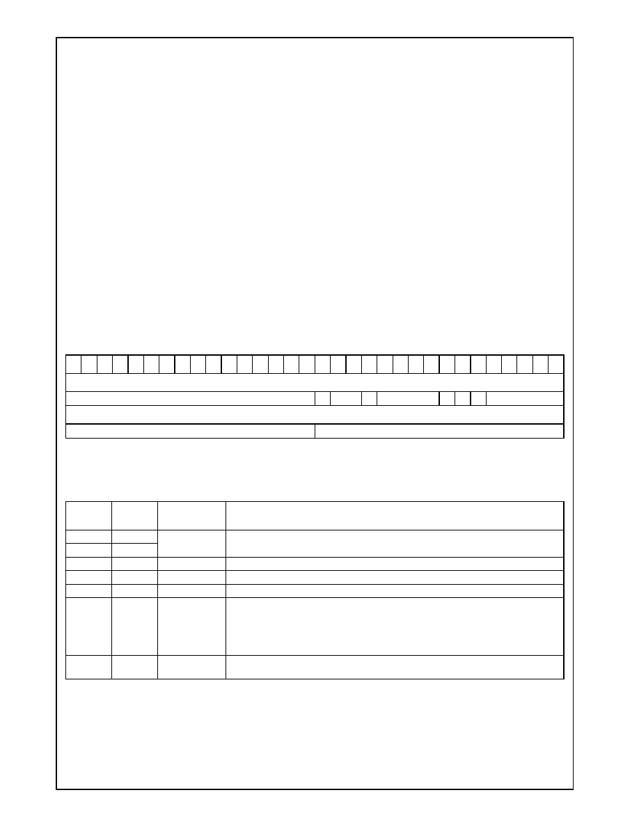
Revision 3.1
69
www.national.com
Processor Programming (
Continued
)
GeodeTM
G
Xm
P
r
ocessor
3.7.5
Gate Descriptors
Four kinds of gate descriptors are used to provide protec-
tion during control transfers: call gates, trap gates, inter-
rupt gates and task gates. (For more information on
protection refer to Section 3.13 "Protection" on page 86.)
Call Gate Descriptor (CGD). Call gates are used to
define legal entry points to a procedure with a higher priv-
ilege level. The call gates are used by CALL and JUMP
instructions in much the same manner as code segment
descriptors. When the CPU decodes an instruction and
sees it refers to a call gate descriptor in the GDT table or a
LDT table, the call gate is used to point to another
descriptor in the table that defines the destination code
segment.
The following privilege levels are tested during the transfer
through the call gate:
∑ CPL = Current Privilege Level
∑ RPL = Segment Selector Field
∑ DPL = Descriptor Privilege Level in the call gate
descriptor.
∑ DPL = Descriptor Privilege Level in the destination
code segment.
The maximum value of the CPL and RPL must be equal
or less than the gate DPL. For a JMP instruction the desti-
nation DPL equals the CPL. For a CALL instruction the
destination DPL is less or equals the CPL.
Conforming Code Segments. Transfer to a procedure
with a higher privilege level can also be accomplished by
bypassing the use of call gates, if the requested proce-
dure is to be executed in a conforming code segment.
Conforming code segments have the C bit set in the
TYPE field in their descriptor.
The bit structure and definitions for gate descriptors are
shown in Tables 3-24 and Table 3-25 on page 69.
Table 3-24. Gate Descriptors
31 30 29 28 27 26 25 24 23 22 21 20 19 18 17 16 15 14 13 12 11 10
9
8
7
6
5
4
3
2
1
0
Memory Offset +4
OFFSET[31:16]
P
DPL
0
TYPE
0
0
0
PARAMETERS
Memory Offset +0
SELECTOR[15:0]
OFFSET[15:0]
Table 3-25. Gate Descriptors Bit Definitions
Bit
Memory
Offset
Name
Description
31:16
+4
OFFSET
Offset: Offset used during a call gate to calculate the branch target.
15:0
+0
31:16
+0
SELECTOR
Segment Selector
15
+4
P
Segment Present
14:13
+4
DPL
Descriptor Privilege Level
11:8
+4
TYPE
Segment Type:
0100 = 16-bit call gate
1100 = 32-bit call gate
0101 = Task gate
1110 = 32-bit interrupt gate
0110 = 16-bit interrupt gate
1111 = 32-bit trap gate
0111 = 16-bit trap gate
4:0
+4
PARAMETERS
Parameters: Number of parameters to copy from the caller's stack to the called proce-
dure's stack.

www.national.com
70
Revision 3.1
Processor Programming (
Continued
)
GeodeTM
G
Xm
Pr
ocessor
3.8
MULTITASKING AND TASK STATE SEGMENTS
The CPU enables rapid task switching using JMP and
CALL instructions that refer to Task State Segments
(TSS). During a switch, the complete task state of the cur-
rent task is stored in its TSS, and the task state of the
requested task is loaded from its TSS. The TSSs are
defined through special segment descriptors and gates.
The Task Register (TR) holds 16-bit descriptors that con-
tain the base address and segment limit for each task
state segment. The TR is loaded and stored via the LTR
and STR instructions, respectively. The TR can only be
accessed only during protected mode and can be loaded
when the privilege level is 0 (most privileged). When the
TR is loaded, the TR selector field indexes a TSS descrip-
tor that must reside in the Global Descriptor Table (GDT).
Only the 16-bit selector of a TSS descriptor in the TR is
accessible. The BASE, TSS LIMT and ACCESS RIGHT
fields are program invisible.
During task switching, the processor saves the current
CPU state in the TSS before starting a new task. The TSS
can be either a 386/486-type 32-bit TSS (see Table 3-26) or a
286-type 16-bit TSS (see Table 3-27 on page 71).
Task Gate Descriptors. A task gate descriptor provides
controlled access to the descriptor for a task switch. The
DPL of the task gate is used to control access. The selec-
tor's RPL and the CPL of the procedure must be a higher
level (numerically less) than the DPL of the descriptor.
The RPL in the task gate is not used.
The I/O Map Base Address field in the 32-bit TSS points
to an I/O permission bit map that often follows the TSS at
location +68h.
Table 3-26. 32-Bit Task State Segment (TSS) Table
31
16 15
0
I/O Map Base Address
0
0
0
0
0
0
0
0
0
0
0
0
0
0
0
T
+64h
0
0
0
0
0
0
0
0
0
0
0
0
0
0
0
0
Selector for Task's LDT
+60h
0
0
0
0
0
0
0
0
0
0
0
0
0
0
0
0
GS
+5Ch
0
0
0
0
0
0
0
0
0
0
0
0
0
0
0
0
FS
+58h
0
0
0
0
0
0
0
0
0
0
0
0
0
0
0
0
DS
+54h
0
0
0
0
0
0
0
0
0
0
0
0
0
0
0
0
SS
+50h
0
0
0
0
0
0
0
0
0
0
0
0
0
0
0
0
CS
+4Ch
0
0
0
0
0
0
0
0
0
0
0
0
0
0
0
0
ES
+48h
EDI
+44h
ESI
+40h
EBP
+3Ch
ESP
+38h
EBX
+34h
EDX
+30h
ECX
+2Ch
EAX
+28h
EFLAGS
+24h
EIP
+20h
CR3
+1Ch
0
0
0
0
0
0
0
0
0
0
0
0
0
0
0
0
SS for CPL = 2
+18h
ESP for CPL = 2
+14h
0
0
0
0
0
0
0
0
0
0
0
0
0
0
0
0
SS for CPL = 1
+10h
ESP for CPL = 1
+Ch
0
0
0
0
0
0
0
0
0
0
0
0
0
0
0
0
SS for CPL = 0
+8h
ESP for CPL = 0
+4h
0
0
0
0
0
0
0
0
0
0
0
0
0
0
0
0
Back Link (Old TSS Selector)
+0h
Note: 0 = Reserved
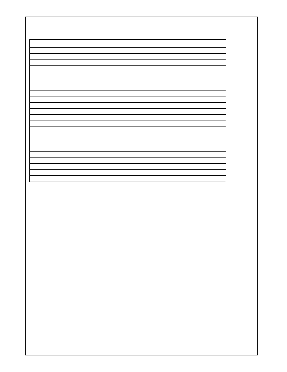
Revision 3.1
71
www.national.com
Processor Programming (
Continued
)
GeodeTM
G
Xm
P
r
ocessor
Table 3-27. 16-Bit Task State Segment (TSS) Table
15
0
Selector for Task's LDT
+2Ah
DS
+28h
SS
+26h
CS
+24h
ES
+22h
DI
+20h
SI
+1Eh
BP
+1Ch
SP
+1Ah
BX
+18h
DX
+16h
CX
+14h
AX
+12h
EFLAGS
+10h
IP
+Eh
SS for Privilege Level 0
+Ch
SP for Privilege Level 1
+Ah
SS for Privilege Level 1
+8h
SP for Privilege Level 1
+6h
SS for Privilege Level 0
+4h
SP for Privilege Level 0
+2h
Back Link (Old TSS Selector)
+0h
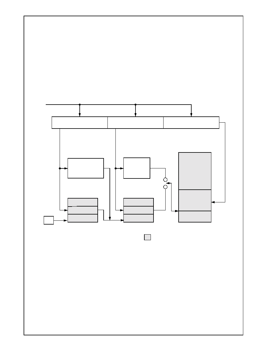
www.national.com
72
Revision 3.1
Processor Programming (
Continued
)
GeodeTM
G
Xm
Pr
ocessor
3.9
PAGING MECHANISM
The paging mechanism translates a linear address to its
corresponding physical address. If the required page is
not currently present in RAM, an exception is generated.
When the operating system services the exception, the
required page can be loaded into memory and the instruc-
tion restarted. Pages are either 4 KB or 1 MB in size. The
CPU defaults to 4 KB pages that are aligned to 4 KB
boundaries.
A page is addressed by using two levels of tables as illus-
trated in Figure 3-8. Bits[31:22] of the 32-bit linear
address, the Directory Table Index (DTI) are used to
locate an entry in the page directory table. The page
directory table acts as a 32-bit master index to up to 1 K
individual second-level page tables. The selected entry in
the page directory table, referred to as the directory table
entry (DTE), identifies the starting address of the second-
level page table. The page directory table itself is a page
and is, therefore, aligned to a 4 KB boundary. The physi-
cal address of the current page directory table is stored in
the CR3 control register, also referred to as the Page
Directory Base Register (PDBR).
Figure 3-8. Paging Mechanism
Directory Table Index
(DTI)
Page Table Index
(PTI)
Page Frame Offset
(PFO)
31
22 21
12 11
0
Linear
Address
DTE Cache
2-Entry
Fully Associative
Main TLB
32-Entry
4-Way Set
Associative
DTE
0
4 KB
PTE
0
4 KB
Physical Page
4 GB
-4 KB
-0
0
External Memory
Directory Table
Page Table
Memory
CR3
Control
Register
1
0
31
0
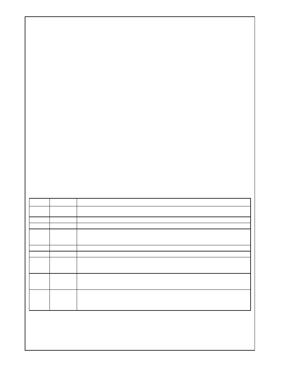
Revision 3.1
73
www.national.com
Processor Programming (
Continued
)
GeodeTM
G
Xm
P
r
ocessor
Bits [21:12] of the 32-bit linear address, referred to as the
Page Table Index (PTI), locate a 32-bit entry in the sec-
ond-level page table. This Page Table Entry (PTE) con-
tains the base address of the desired page frame. The
second-level page table addresses up to 1K individual
page frames. A second-level page table is 4 KB in size
and is itself a page. Bits [11:0] of the 32-bit linear address,
the Page Frame Offset (PFO), locate the desired physical
data within the page frame.
Since the page directory table can point to 1 K page
tables, and each page table can point to 1 K page frames,
a total of 1 M page frames can be implemented. Since
each page frame contains 4 KB, up to 4 GB of virtual
memory can be addressed by the CPU with a single page
directory table.
Along with the base address of the page table or the page
frame, each directory table entry or page table entry con-
tains attribute bits and a present bit as illustrated in Table
3-28.
If the present bit (P) is set in the DTE, the page table is
present and the appropriate page table entry is read. If P
= 1 in the corresponding PTE (indicating that the page is
in memory), the accessed and dirty bits are updated, if
necessary, and the operand is fetched. Both accessed
bits are set (DTE and PTE), if necessary, to indicate that
the table and the page have been used to translate a linear
address. The dirty bit (D) is set before the first write is made
to a page.
The present bits must be set to validate the remaining bits
in the DTE and PTE. If either of the present bits are not
set, a page fault is generated when the DTE or PTE is
accessed. If P = 0, the remaining DTE/PTE bits are avail-
able for use by the operating system. For example, the
operating system can use these bits to record where on
the hard disk the pages are located. A page fault is also
generated if the memory reference violates the page pro-
tection attributes.
Translation Look-Aside Buffer
The translation look-aside buffer (TLB) is a cache for the
paging mechanism and replaces the two-level page table
lookup procedure for TLB hits. The TLB is a four-way set
associative 32-entry page table cache that automatically
keeps the most commonly used page table entries in the
processor. The 32-entry TLB, coupled with a 4 K page
size, results in coverage of 128 KB of memory addresses.
The TLB must be flushed when entries in the page tables
are changed. The TLB is flushed whenever the CR3 regis-
ter is loaded. An individual entry in the TLB can be flushed
using the INVLPG instruction.
DTE Cache
The DTE cache caches the two most recent DTEs so that
future TLB misses only require a single page table read to
calculate the physical address. The DTE cache is dis-
abled following reset and can be enabled by setting the
DTE_EN bit in CCR4[4] (Index E8h).
Table 3-28. Directory Table Entry (DTE) and Page Table Entry (PTE)
Bit
Name
Description
31:12
BASE
ADDRESS
Base Address: Specifies the base address of the page or page table.
11:9
AVAILABLE
Available: Undefined and Available to the Programmer
8:7
RSVD
Reserved: Unavailable to programmer
6
D
Dirty Bit:
PTE format -- If = 1: Indicates that a write access has occurred to the page.
DTE format -- Reserved.
5
A
Accessed Flag: If set, indicates that a read access or write access has occurred to the page.
4:3
RSVD
Reserved: Set to 0.
2
U/S
User/Supervisor Attribute:
If = 1: Page is accessible by User at privilege level 3.
If = 0: Page is accessible by Supervisor only when CPL
2.
1
W/R
Write/Read Attribute:
If = 1: Page is writable.
If = 0: Page is read only.
0
P
Present Flag:
If = 1: The page is present in RAM and the remaining DTE/PTE bits are validated
If = 0: The page is not present in RAM and the remaining DTE/PTE bits are available for use by the pro-
grammer.

www.national.com
74
Revision 3.1
Processor Programming (
Continued
)
GeodeTM
G
Xm
Pr
ocessor
3.10 INTERRUPTS AND EXCEPTIONS
The processing of either an interrupt or an exception
changes the normal sequential flow of a program by trans-
ferring program control to a selected service routine.
Except for SMM interrupts, the location of the selected
service routine is determined by one of the interrupt vec-
tors stored in the interrupt descriptor table.
True interrupts are hardware interrupts and are generated
by signal sources external to the processor. All exceptions
(including so-called software interrupts) are produced inter-
nally by the processor.
3.10.1 Interrupts
External events can interrupt normal program execution
by using one of the three interrupt pins on the GXm pro-
cessor:
∑ Non-maskable Interrupt (NMI pin)
∑ Maskable Interrupt (INTR pin)
∑ SMM Interrupt (SMI# pin)
For most interrupts, program transfer to the interrupt rou-
tine occurs after the current instruction has been com-
pleted. When the execution returns to the original
program, it begins immediately following the interrupted
instruction.
The NMI interrupt cannot be masked by software and
always uses interrupt vector 2 to locate its service routine.
Since the interrupt vector is fixed and is supplied inter-
nally, no interrupt acknowledge bus cycles are performed.
This interrupt is normally reserved for unusual situations
such as parity errors and has priority over INTR interrupts.
Once NMI processing has started, no additional NMIs are
processed until an IRET instruction is executed, typically
at the end of the NMI service routine. If NMI is re-asserted
before execution of the IRET instruction, one and only one
NMI rising edge is stored and then processed after execu-
tion of the next IRET.
During the NMI service routine, maskable interrupts may
be enabled. If an unmasked INTR occurs during the NMI
service routine, the INTR is serviced and execution
returns to the NMI service routine following the next IRET.
If a HALT instruction is executed within the NMI service
routine, the CPU restarts execution only in response to
RESET, an unmasked INTR or a System Management
Mode (SMM) interrupt. NMI does not restart CPU execu-
tion under this condition.
The INTR interrupt is unmasked when the Interrupt
Enable Flag (IF, bit 9) in the EFLAGS register is set to 1.
Except for string operations, INTR interrupts are acknowl-
edged between instructions. Long string operations have
interrupt windows between memory moves that allow
INTR interrupts to be acknowledged.
When an INTR interrupt occurs, the processor performs
an interrupt-acknowledge bus cycle. During this cycle, the
CPU reads an 8-bit vector that is supplied by an external
interrupt controller. This vector selects which of the 256
possible interrupt handlers will be executed in response to
the interrupt.
The SMM interrupt has higher priority than either INTR or
NMI. After SMI# is asserted, program execution is passed
to an SMI service routine that runs in SMM address space
reserved for this purpose. The remainder of this section
does not apply to the SMM interrupts. SMM interrupts are
described in greater detail later in this section.
3.10.2 Exceptions
Exceptions are generated by an interrupt instruction or a
program error. Exceptions are classified as traps, faults or
aborts depending on the mechanism used to report them
and the restartability of the instruction which first caused
the exception.
A Trap exception is reported immediately following the
instruction that generated the trap exception. Trap excep-
tions are generated by execution of a software interrupt
instruction (INTO, INT3, INTn, BOUND), by a single-step
operation or by a data breakpoint.
Software interrupts can be used to simulate hardware
interrupts. For example, an INTn instruction causes the
processor to execute the interrupt service routine pointed
to by the nth vector in the interrupt table. Execution of the
interrupt service routine occurs regardless of the state of
the IF flag (bit 9) in the EFLAGS register.
The one byte INT3, or breakpoint interrupt (vector 3), is a
particular case of the INTn instruction. By inserting this
one byte instruction in a program, the user can set break-
points in the code that can be used during debug.

Revision 3.1
75
www.national.com
Processor Programming (
Continued
)
GeodeTM
G
Xm
P
r
ocessor
Single-step operation is enabled by setting the TF bit (bit
8) in the EFLAGS register. When TF is set, the CPU gen-
erates a debug exception (vector 1) after the execution of
every instruction. Data breakpoints also generate a debug
exception and are specified by loading the debug regis-
ters (DR0-DR7) with the appropriate values.
A Fault exception is reported before completion of the
instruction that generated the exception. By reporting the
fault before instruction completion, the processor is left in
a state that allows the instruction to be restarted and the
effects of the faulting instruction to be nullified. Fault
exceptions include divide-by-zero errors, invalid opcodes,
page faults and coprocessor errors. Debug exceptions
(vector 1) are also handled as faults (except for data
breakpoints and single-step operations). After execution
of the fault service routine, the instruction pointer points to
the instruction that caused the fault.
An Abort exception is a type of fault exception that is
severe enough that the CPU cannot restart the program at
the faulting instruction. The double fault (vector 8) is the
only abort exception that occurs on the processor.
3.10.3 Interrupt Vectors
When the processor services an interrupt or exception,
the current program's instruction pointer and flags are
pushed onto the stack to allow resumption of execution of
the interrupted program. In protected mode, the processor
also saves an error code for some exceptions. Program
control is then transferred to the interrupt handler (also
called the interrupt service routine). Upon execution of an
IRET at the end of the service routine, program execution
resumes at the instruction pointer address saved on the
stack when the interrupt was serviced.
3.10.3.1 Interrupt Vector Assignments
Each interrupt (except SMI#) and exception is assigned
one of 256 interrupt vector numbers as shown in Table 3-
29. The first 32 interrupt vector assignments are defined
or reserved. INT instructions acting as software interrupts
may use any of interrupt vectors, 0 through 255.
The non-maskable hardware interrupt (NMI) is assigned
vector 2. Illegal opcodes including faulty FPU instructions
will cause an illegal opcode exception, interrupt vector 6.
NMI interrupts are enabled by setting bit 2 of the CCR7
register (Index EBh[2] = 1, see Table 3-11 on page 49 for
register format).
In response to a maskable hardware interrupt (INTR), the
processor issues interrupt acknowledge bus cycles used to
read the vector number from external hardware. These vec-
tors should be in the range 32 to 255 as vectors 0 to 31 are
predefined. In PCs, vectors 8 through 15 are used.
3.10.3.2 Interrupt Descriptor Table
The interrupt vector number is used by the processor to
locate an entry in the interrupt descriptor table (IDT). In
real mode, each IDT entry consists of a four-byte far
pointer to the beginning of the corresponding interrupt
service routine. In protected mode, each IDT entry is an
8-byte descriptor. The Interrupt Descriptor Table Register
(IDTR) specifies the beginning address and limit of the
IDT. Following reset, the IDTR contains a base address of
0h with a limit of 3FFh.
The IDT can be located anywhere in physical memory as
determined by the IDTR. The IDT may contain different
types of descriptors: interrupt gates, trap gates and task
gates. Interrupt gates are used primarily to enter a hard-
ware interrupt handler. Trap gates are generally used to
enter an exception handler or software interrupt handler. If
an interrupt gate is used, the Interrupt Enable Flag (IF) in
the EFLAGS register is cleared before the interrupt han-
dler is entered. Task gates are used to make the transition
to a new task.
Table 3-29. Interrupt Vector Assignments
Interrupt
Vector
Function
Exception
Type
0
Divide error
Fault
1
Debug exception
Trap/Fault*
2
NMI interrupt
3
Breakpoint
Trap
4
Interrupt on overflow
Trap
5
BOUND range exceeded
Fault
6
Invalid opcode
Fault
7
Device not available
Fault
8
Double fault
Abort
9
Reserved
10
Invalid TSS
Fault
11
Segment not present
Fault
12
Stack fault
Fault
13
General protection fault
Trap/Fault
14
Page fault
Fault
15
Reserved
16
FPU error
Fault
17
Alignment check exception
Fault
18:31
Reserved
32:55
Maskable hardware interrupts
Trap
0:255
Programmed interrupt
Trap
Note: *Data breakpoints and single steps are traps. All other
debug exceptions are faults.

www.national.com
76
Revision 3.1
Processor Programming (
Continued
)
GeodeTM
G
Xm
Pr
ocessor
3.10.4 Interrupt and Exception Priorities
As the CPU executes instructions, it follows a consistent
policy for prioritizing exceptions and hardware interrupts.
The priorities for competing interrupts and exceptions are
listed in Table 3-30. SMM interrupts always take prece-
dence. Debug traps for the previous instruction and next
instructions are handled as the next priority. When NMI
and maskable INTR interrupts are both detected at the
same instruction boundary, the GXm processor services
the NMI interrupt first.
The CPU checks for exceptions in parallel with instruction
decoding and execution. Several exceptions can result
from a single instruction. However, only one exception is
generated upon each attempt to execute the instruction.
Each exception service routine should make the appropri-
ate corrections to the instruction and then restart the
instruction. In this way, exceptions can be serviced until
the instruction executes properly.
The CPU supports instruction restart after all faults,
except when an instruction causes a task switch to a task
whose task state segment (TSS) is partially not present. A
TSS can be partially not present if the TSS is not page
aligned and one of the pages where the TSS resides is
not currently in memory.
Table 3-30. Interrupt and Exception Priorities
Priority
Description
Notes
0
Warm Reset.
Caused by the assertion of WM_RST.
1
SMM hardware interrupt.
SMM interrupts are caused by SMI# asserted and always have
highest priority.
2
Debug traps and faults from previous instruction.
Includes single-step trap and data breakpoints specified in the
debug registers.
3
Debug traps for next instruction.
Includes instruction execution breakpoints specified in the debug
registers.
4
Non-maskable hardware interrupt.
Caused by NMI asserted.
5
Maskable hardware interrupt.
Caused by INTR asserted and IF = 1.
6
Faults resulting from fetching the next instruction.
Includes segment not present, general protection fault and page
fault.
7
Faults resulting from instruction decoding.
Includes illegal opcode, instruction too long, or privilege violation.
8
WAIT instruction and TS = 1 and MP = 1.
Device not available exception generated.
9
ESC instruction and EM = 1 or TS = 1.
Device not available exception generated.
10
Floating point error exception.
Caused by unmasked floating point exception with NE = 1.
11
Segmentation faults (for each memory reference
required by the instruction) that prevent transferring
the entire memory operand.
Includes segment not present, stack fault, and general protection
fault.
12
Page Faults that prevent transferring the entire
memory operand.
13
Alignment check fault.
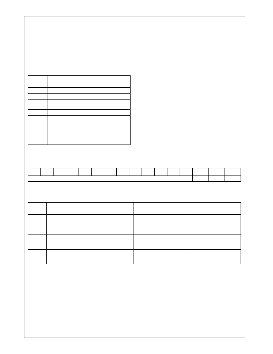
Revision 3.1
77
www.national.com
Processor Programming (
Continued
)
GeodeTM
G
Xm
P
r
ocessor
3.10.5 Exceptions in Real Mode
Many of the exceptions described in Table 3-29 on page
75 are not applicable in real mode. Exceptions 10, 11, and
14 do not occur in real mode. Other exceptions have
slightly different meanings in real mode as listed in Table
3-31.
3.10.6 Error Codes
When operating in protected mode, the following exceptions
generate a 16-bit error code:
∑ Double Fault
∑ Alignment Check
∑ Invalid TSS
∑ Segment Not Present
∑ Stack Fault
∑ General Protection Fault
∑ Page Fault
The error code format and bit definitions are shown in
Table 3-32. Bits [15:3] (selector index) are not meaningful
if the error code was generated as the result of a page
fault. The error code is always zero for double faults and
alignment check exceptions.
Table 3-31. Exception Changes in Real Mode
Vector
Number
Protected Mode
Function
Real Mode
Function
8
Double fault.
Interrupt table limit overrun.
10
Invalid TSS.
Does not occur.
11
Segment not
present.
Does not occur.
12
Stack fault.
SS segment limit overrun.
13
General protection
fault.
CS, DS, ES, FS, GS seg-
ment limit overrun. In pro-
tected mode, an error is
pushed. In real mode, no
error is pushed.
14
Page fault.
Does not occur.
Table 3-32. Error Codes
15
14
13
12
11
10
9
8
7
6
5
4
3
2
1
0
Selector Index
S2
S1
S0
Table 3-33. Error Code Bit Definitions
Fault
Type
Selector Index
(Bits 15:3)
S2 (Bit 2)
S1 (Bit 1)
S0 (Bit 0)
Page
Fault
Reserved.
Fault caused by:
0 = Not present page
1 = Page-level protection
violation
Fault occurred during:
0 = Read access
1 = Write access
Fault occurred during
0 = Supervisor access
1 = User access.
IDT Fault
Index of faulty IDT
selector.
Reserved
1
If = 1, exception occurred while
trying to invoke exception or
hardware interrupt handler.
Segment
Fault
Index of faulty
selector.
TI bit of faulty selector
0
If =1, exception occurred while
trying to invoke exception or
hardware interrupt handler.
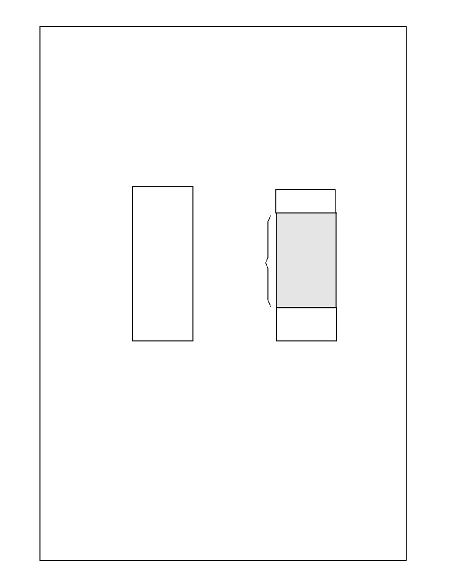
www.national.com
78
Revision 3.1
Processor Programming (
Continued
)
GeodeTM
G
Xm
Pr
ocessor
3.11 SYSTEM MANAGEMENT MODE
System Management Mode (SMM) is usually employed
for system power management or software-transparent
emulation of I/O peripherals. SMM mode is entered
through a hardware signal "System Management Inter-
rupt" (SMI# pin) that has a higher priority than any other
interrupt, including NMI. An SMM interrupt can also be
triggered from software using an SMINT instruction. Fol-
lowing an SMM interrupt, portions of the CPU state are
automatically saved, SMM mode is entered, and program
execution begins at the base of SMM address space (Fig-
ure 3-9).
The GXm processor extends System Management Mode
(SMM) to support the virtualization of many devices,
including VGA video. The SMM mechanism can be trig-
gered not only by I/O activity, but by access to selected
memory regions. For example, SMM interrupts are gener-
ated when VGA addresses are accessed. As will be
described, other SMM enhancements have reduced SMM
overhead and improved virtualization-software perfor-
mance
Figure 3-9. System Management Memory Address Space
FFFFFFFFh
00000000h
Non-SMM
SMM
Potential
SMM Address
Space
Physical
Memory Space
FFFFFFFFh
00000000h
4 KB to 32 MB
Physical Memory
4 GB
Defined
SMM
Address
Space

Revision 3.1
79
www.national.com
Processor Programming (
Continued
)
GeodeTM
G
Xm
P
r
ocessor
3.11.1 SMM Enhancements
Eight SMM instructions have been added to the x86
instruction set that permit initiating SMM through software
and saving and restoring the total CPU state when in
SMM.
The SMM header now:
∑ Stores 32-bits memory addresses.
∑ Stores 32-bit memory data.
∑ Differentiates memory and I/O accesses.
∑ Indicates if an SMM interrupt was generated by access
to a VGA region.
The SMM service code is now cacheable. An SMAR reg-
ister specifies the SMM region code base and limit. An
SMHR register specifies the physical address for the
SMM header. The SMI_NEST bit enables the nesting of
SMM interrupts.
3.11.2 SMM Operation
SMM execution flow is summarized in Figure 3-10. Enter-
ing SMM requires the assertion of the SMI# pin for at least
two SYSCLK periods or execution of the SMINT instruction.
For the SMI# signal or SMINT instruction to be recog-
nized, configuration register bits must be set as shown in
Table 3-34. (The configuration registers are discussed in
detail in Section 3.3.2.2 "Configuration Registers" on page
47.)
After triggering an SMM through the SMI# pin or a SMINT
instruction, selected CPU state information is automati-
cally saved in the SMM memory space header located at
the top of SMM memory space. After saving the header,
the CPU enters real mode and begins executing the SMM
service routine starting at the SMM memory region base
address.
The SMM service routine is user definable and may con-
tain system or power management software. If the power
management software forces the CPU to power down or if
the SMM service routine modifies more registers than are
automatically saved, the complete CPU state information
should be saved.
Figure 3-10. SMM Execution Flow
Table 3-34. SMI# and SMINT Recognition
Requirements
Register Bits
SMI#
SMINT
USE_SMI, CCR1[1] (Index C1h)
1
1
SMAC, CCR1[2] (Index C1h)
0
1
SIZE[3:0], SMAR3[3:0] (Index CFh)
> 0
> 0
SMI# Sampled Active or
SMINT Instruction Executed
CPU State Stored in SMM
Address Space Header
Program Flow Transfers
to SMM Address Space
CPU Enters Real Mode
Execution Begins at SMM
Address Space Base Address
RSM Instruction Restores CPU
State Using Header Information
Normal Execution Resumes
www.national.com
80
Revision 3.1
Processor Programming (
Continued
)
GeodeTM
G
Xm
Pr
ocessor
3.11.3 The SMI# Pin
External chipsets can generate an SMI based on numer-
ous asynchronous events, including power management
timers, I/O address trapping, external devices, audio FIFO
events, and others. Since SMI# is edge sensitive, the
chipset must generate an edge for each of the events
above, requiring arbitration and storage of multiple SMM
events. These functions are provided by the CS5530 I/O
companion device. The processor generates an SMI
when the external pin changes from high-to-low or when
an RSM occurs if SMI# has not remained low since the
initiation of the previous SMI.
3.11.4 SMM Configuration Registers
The SMAR register specifies the base location of SMM
code region and its size limit. This SMAR register is identi-
cal to many of the National Semconductor processors.
A new configuration control register called SMHR has
been added to specify the 32-bit physical address of the
SMM header. The SMHR address must be 32-bit aligned
as the bottom two bits are ignored by the microcode.
Hardware will detect write operations to SMHR, and sig-
nal the microcode to recompute the header address.
Access to these registers is enabled by MAPEN (Index
C3h[4]).
The SMAR register writes to the SMM header when the
SMAR register is changed. For this reason, changes to
the SMAR register should be completed prior to setting up
the SMM header. The configuration registers bit formats
are detailed in Table 3-11 on page 49.
3.11.5 SMM Memory Space Header
Tables 3-35 and
show the SMM header. A memory
address field has been added to the end (offset ≠40h) of
the header for the GXm processor. Memory data will be
stored overlapping the I/O data, since these events can-
not occur simultaneously. The I/O address is valid for both
IN and OUT instructions, and I/O data is valid only for
OUT. The memory address is valid for read and write
operations, and memory data is valid only for write opera-
tions.
With every SMI interrupt or SMINT instruction, selected
CPU state information is automatically saved in the SMM
memory space header located at the top of SMM address
space. The header contains CPU state information that is
modified when servicing an SMM interrupt. Included in
this information are two pointers. The current IP points to
the instruction executing when the SMI was detected, but
it is valid only for an internal I/O SMI.
The Next IP points to the instruction that will be executed
after exiting SMM. The contents of Debug Register 7
(DR7), the Extended FLAGS Register (EFLAGS), and
Control Register 0 (CR0) are also saved. If SMM has
been entered due to an I/O trap for a REP INSx or REP
OUTSx instruction, the Current IP and Next IP fields con-
tain the same addresses. In addition, the I and P fields con-
tain valid information.
If entry into SMM is the result of an I/O trap, it is useful for
the programmer to know the port address, data size and
data value associated with that I/O operation. This informa-
tion is also saved in the header and is valid only if SMI# is
asserted during an I/O bus cycle. The I/O trap information is
not restored within the CPU when executing a RSM instruction.
Table 3-35. SMM Memory Space Header
Mem.
Offset 31 30 29 28 27 26 25 24 23 22 21 20 19 18 17 16 15 14 13 12 11 10
9
8
7
6
5
4
3
2
1
0
-4h
DR7
≠8h
EFLAGS
≠Ch
CR0
≠10h
Current IP
≠14h
Next IP
≠18h
RSVD
CS Selector
≠1Ch
CS Descriptor [63:32]
≠20h
CS Descriptor [31:0]
≠24h
RSVD
RSVD
N
V
X
M
H
S
P
I
C
≠28h
I/O Data Size
I/O Address [15:0]
≠2Ch
I/O or Memory Data [31:0] (Note)
≠30h
Restored ESI or EDI
≠32h
Memory Address [31:0]
Note: Check the M bit at offset 24h to determine if the data is memory or I/O.
Revision 3.1
81
www.national.com
Processor Programming (
Continued
)
GeodeTM
G
Xm
P
r
ocessor
Table 3-36. SMM Memory Space Header Description
Name
Description
Size
DR7
Debug Register 7: The contents of Debug Register 7.
4 Bytes
EFLAGS
Extended FLAGS Register: The contents of Extended FLAGS Register.
4 Bytes
CR0
Control Register 0: The contents of Control Register 0.
4 Bytes
Current IP
Current Instruction Pointer: The address of the instruction executed prior to servicing SMM
interrupt.
4 Bytes
Next IP
Next Instruction Pointer: The address of the next instruction that will be executed after exiting
SMM.
4 Bytes
CS Selector
Code Segment Selector: Code segment register selector for the current code segment.
2 Bytes
CS Descriptor
Code Segment Descriptor: Encoded descriptor bits for the current code segment.
8 Bytes
N
Nested SMI Status: Flag that determines whether an SMI occurred during SMM (i.e., nested)
1 Bit
V
SoftVGA SMI Status: SMI was generated by an access to VGA region.
1 Bit
X
External SMI Status:
If = 1: SMI generated by external SMI# pin
If = 0: SMI internally generated by Internal Bus Interface Unit.
1 Bit
M
Memory or I/O Access: 0 = I/O access; 1 = Memory access.
1 Bit
H
Halt Status: Indicates that the processor was in a halt or shutdown prior to servicing the SMM
interrupt.
1 Bit
S
Software SMM Entry Indicator:
If = 1: Current SMM is the result of an SMINT instruction.
If = 0: Current SMM is not the result of an SMINT instruction.
1 Bit
P
REP INSx/OUTSx Indicator:
If = 1: Current instruction has a REP prefix.
If = 0: Current instruction does not have a REP prefix.
1 Bit
I
IN, INSx, OUT, or OUTSx Indicator:
If = 1: Current instruction performed is an I/O WRITE.
If = 0: Current instruction performed is an I/O READ.
1 Bit
C
CS Writable: Code Segment Writable
If = 1: CS is writable
If = 0: CS is not writable
1 Bit
I/O Data Size
Indicates size of data for the trapped I/O cycle:
01h = byte
03h = word
0Fh = DWORD
2 Bytes
I/O Address
Processor port used for the trapped I/O cycle.
2 Bytes
I/O or Memory Data
Data associated with the trapped I/O or memory cycleS.
4 Bytes
Restored ESI or EDI
Restored ESI or EDI Value: Used when it is necessary to repeat a REP OUTSx or REP INSx
instruction when one of the I/O cycles caused an SMI# trap.
4 Bytes
Memory Address
Physical address of the operation that caused the SMI.
4 Bytes
Note: INSx = INS, INSB, INSW or INSD instruction.
OUTSx = OUTS, OUTSB, OUTSW and OUTSD instruction.
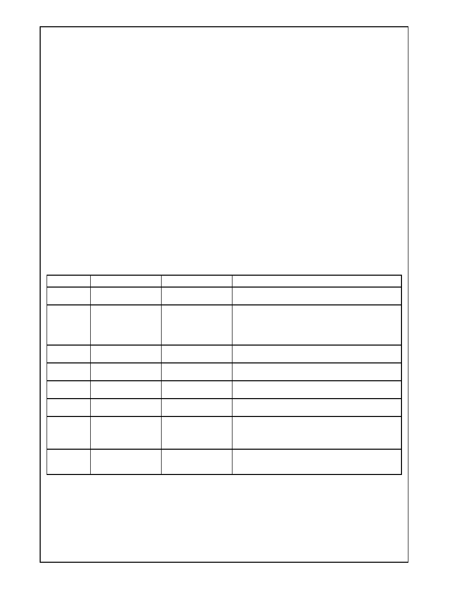
www.national.com
82
Revision 3.1
Processor Programming (
Continued
)
GeodeTM
G
Xm
Pr
ocessor
3.11.6 SMM Instructions
The GXm processor core automatically saves the minimal
amount of CPU state information when entering an SMM
cycle that allows fast SMM service-routine entry and exit.
After entering the SMM service routine, the MOV, SVDC,
SVLDT and SVTS instructions can be used to save the
complete CPU state information. If the SMM service rou-
tine modifies more state information than is automatically
saved or if it forces the CPU to power down, the complete
CPU state information must be saved. Since the CPU is a
static device, its internal state is retained when the input
clock is stopped. Therefore, an entire CPU-state save is
not necessary before stopping the input clock.
The SMM instructions, listed in Table 3-37, can be exe-
cuted only if all the conditions listed below are met.
1)
USE_SMI = 1.
2)
SMAR SIZE > 0.
3)
Current Privilege level = 0.
4)
SMAC bit is high or the CPU is in an SMI service
routine.
If any one of the conditions above is not met and an
attempt is made to execute an SVDC, RSDC, SVLDT,
RSLDT, SVTS, RSTS, or RSM instruction, an invalid
opcode exception is generated. The SMM instructions can
be executed outside of defined SMM space provided the
conditions above are met.
The SMINT instruction can be used by software to enter
SMM. The SMINT instruction can only be used outside an
SMM routine if all the conditions listed below are true.
1)
USE_SMI = 1
2)
SMAR size > 0
3)
Current Privilege Level = 0
4)
SMAC = 1
If SMI# is asserted to the CPU during a software SMI, the
hardware SMI# is serviced after the software SMI has
been exited by execution of the RSM instruction.
All the SMM instructions (except RSM and SMINT) save
or restore 80 bits of data, allowing the saved values to
include the hidden portion of the register contents.
Table 3-37. SMM Instruction Set
Instruction
Opcode
Format
Description
SVDC
0F 78h [mod sreg3 r/m]
SVDC mem80, sreg3
Save Segment Register and Descriptor
Saves reg (DS, ES, FS, GS, or SS) to mem80.
RSDC
0F 79h [mod sreg3 r/m]
RSDC sreg3, mem80
Restore Segment Register and Descriptor
Restores reg (DS, ES, FS, GS, or SS) from mem80. Use RSM
to restore CS.
Note: Processing "RSDC CS, Mem80" will produce an excep-
tion.
SVLDT
0F 7Ah [mod 000 r/m]
SVLDT mem80
Save LDTR and Descriptor
Saves Local Descriptor Table (LDTR) to mem80.
RSLDT
0F 7Bh [mod 000 r/m]
RSLDT mem80
Restore LDTR and Descriptor
Restores Local Descriptor Table (LDTR) from mem80.
SVTS
0F 7Ch [mod 000 r/m]
SVTS mem80
Save TSR and Descriptor
Saves Task State Register (TSR) to mem80.
RSTS
0F 7Dh [mod 000 r/m]
RSTS mem80
Restore TSR and Descriptor
Restores Task State Register (TSR) from mem80.
SMINT
0F 38h
SMINT
Software SMM Entry
CPU enters SMM. CPU state information is saved in SMM
memory space header and execution begins at SMM base
address.
RSM
0F AAh
RSM
Resume Normal Mode
Exits SMM. The CPU state is restored using the SMM memory
space header and execution resumes at interrupted point.
Note: smem80 = 80-bit memory location.

Revision 3.1
83
www.national.com
Processor Programming (
Continued
)
GeodeTM
G
Xm
P
r
ocessor
3.11.7 SMM Memory Space
SMM memory space is defined by specifying the base
address and size of the SMM memory space in the SMAR
register. The base address must be a multiple of the SMM
memory space size. For example, a 32 KB SMM memory
space must be located at a 32 KB address boundary. The
memory space size can range from 4 KB to 32 MB. Execu-
tion of the interrupt begins at the base of the SMM memory
space.
SMM memory space accesses are always cacheable,
which allows SMM routines to run faster.
3.11.8 SMI Generation
Virtualization software depends on processor-specific
hardware to generate SMI interrupts for each memory or
I/O access to the device being implemented. The GXm
processor implements SMI generation for VGA accesses.
Memory write operations in regions A0000h to AFFFFh,
B0000h to B7FFFh, and B8000h to BFFFFh generate an
SMI.
Memory reads are not trapped by the GXm processor.
The GXm processor traps I/O addresses for VGA in the
following regions: 3B0h to 3BFh, 3C0h to 3CFh, and 3D0h
to 3DFh. Memory-write trapping is performed during
instruction decode in the processor core. I/O read and
write trapping is implemented in the Internal Bus Interface
Unit of the GXm processor.
The SMI-generation hardware requires two additional
configuration registers to control and mask SMI interrupts
in the VGA memory space: VGACTL and VGAM. The
VGACTL register has a control bit for each address range
shown above. The VGAM register has 32 bits that can
selectively disable 2 KB regions within the VGA memory.
The VGAM applies only to the A0000h-to-AFFFFh region.
If this region is not enabled in VGA_CTL, then the con-
tents of VGAM is ignored. The purpose of VGAM is to pre-
vent SMI from occurring when non-displayed VGA
memory is accessed. This is an enhancement which
improves performance for double-buffered applications.
The format of each register is shown in Chapter 4 of this
document.
3.11.9 SMI Service Routine Execution
Upon entry into SMM, after the SMM header has been
saved, the CR0, EFLAGS, and DR7 registers are set to
their reset values. The Code Segment (CS) register is
loaded with the base, as defined by the SMAR register,
and a limit of 4 GBytes. The SMI service routine then
begins execution at the SMM base address in real mode.
The programmer must save the value of any registers that
may be changed by the SMI service routine. For data
accesses immediately after entering the SMI service rou-
tine, the programmer must use CS as a segment override.
I/O port access is possible during the routine but care
must be taken to save registers modified by the I/O
instructions. Before using a segment register, the register
and the register's descriptor cache contents should be saved
using the SVDC instruction.
Hardware interrupts, INTRs and NMIs, may be serviced
during an SMI service routine. If interrupts are to be ser-
viced while executing in the SMM memory space, the
SMM memory space must be within the address range of
0 to 1 MB to guarantee proper return to the SMI service
routine after handling the interrupt.
INTRs are automatically disabled when entering SMM
since the IF flag (EFLAGS register, bit 9) is set to its reset
value. Once in SMM, the INTR can be enabled by setting
the IF flag. An NMI event in SMM can be enabled by set-
ting NMI_EN high in the CCR3 register (Index C3h[1]). If
NMI is not enabled while in SMM, the CPU latches one
NMI event and services the interrupt after NMI has been
enabled or after exiting SMM through the RSM instruction.
The processor is always in real mode in SMM, but it may
exit to either real or protected mode depending on its
state when SMM was initiated. The IDT (Interrupt Descrip-
tor Table) indicates which state it will exit to.
Within the SMI service routine, protected mode may be
entered and exited as required, and real or protected
mode device drivers may be called.
To exit the SMI service routine, a Resume (RSM) instruc-
tion, rather than an IRET, is executed. The RSM instruc-
tion causes the GXm processor core to restore the CPU
state using the SMM header information and resume exe-
cution at the interrupted point. If the full CPU state was
saved by the programmer, the stored values should be
reloaded before executing the RSM instruction using the
MOV, RSDC, RSLDT and RSTS instructions.
3.11.9.1 SMI Nesting
The SMI mechanism supports nesting of SMI interrupts
through the SMI handler, the SMI_NEST bit in CCR4[6]
(Index E8h), and the Nested SMI Status bit (bit N in the
SMM header, see Table on page 80). Nesting is an impor-
tant capability in allowing high-priority events, such as
audio virtualization, to interrupt lower-priority SMI code for
VGA virtualization or power management. SMI_NEST
controls whether SMI interrupts can occur during SMM.
SMI handlers can optionally set SMI_NEST high to allow
higher-priority SMI interrupts while handling the current
event.
The SMI handler is responsible for managing the SMI
header data for nested SMI interrupts. The SMI header
must be saved before SMI_NEST is set high, and
SMI_NEST must be cleared and its header information
restored before an RSM instruction is executed.
The Nested SMI Status bit has been added to the SMM
header to show whether the current SMI is nested. The
processor sets Nested SMI Status high if the processor
was in SMM when the SMI was taken. The processor
uses Nested SMI Status on exit to determine whether the
processor should stay in SMM.
When SMI nesting is disabled, the processor holds off
external SMI interrupts until the currently executing SMM
code exits. When SMI nesting is enabled, the processor
can proceed with the SMI. The SMI handler will guarantee

www.national.com
84
Revision 3.1
Processor Programming (
Continued
)
GeodeTM
G
Xm
Pr
ocessor
that no internal SMIs are generated in SMM, so the pro-
cessor ignores such events. If the internal and external
SMI signals are received simultaneously, then the internal
SMI is given priority to avoid losing the event.
The state diagram of the SMI_NEST and Nested SMI Sta-
tus bits are shown in Figure 3-11 with each state
explained next.
A. When the processor is outside of SMM, Nested SMI
Status is always clear and SMI_NEST is set high.
B. The first-level SMI interrupt is received by the
processor. The microcode clears SMI_NEST, sets
Nested SMI Status high and saves the previous
value of Nested SMI Status (0) in the SMI header.
C. The first-level SMI handler saves the header and
sets SMI_NEST high to re-enable SMI interrupts
from SMM.
D. A second-level (nested) SMI interrupt is received by
the processor. This SMI is taken even though the
processor is in SMM because the SMI_NEST bit is
set high. The microcode clears SMI_NEST, sets
Nested SMI Status high and saves the previous
value of Nested SMI Status (1) in the SMI header.
E. The second-level SMI handler saves the header and
sets SMI_NEST to re-enable SMI interrupts within
SMM. Another level of nesting could occur during
this period.
F. The second-level SMI handler clears SMI_NEST to
disable SMI interrupts, then restores its SMI header.
G. The second-level SMI handler executes an RSM.
The microcode sets SMI_NEST, and restores the
Nested SMI Status (1) based on the SMI header.
H. The first-level SMI handler clears SMI_NEST to
disable SMI interrupts, then restores its SMI header.
I. The first-level SMI handler executes an RSM. The
microcode sets SMI_NEST high and restores the
Nested SMI Status (0) based on the SMI header.
When the processor is outside of SMM, Nested SMI Sta-
tus is always clear and SMI_NEST is set high.
Figure 3-11. SMI Nesting State Machine
SMI_NEST
Nested SMI Status
A
B
C
D
E
F
G
H
I

Revision 3.1
85
www.national.com
Processor Programming (
Continued
)
GeodeTM
G
Xm
P
r
ocessor
3.11.9.2 CPU States Related to SMM and Suspend
Mode
The state diagram shown in Figure 3-12 illustrates the var-
ious CPU states associated with SMM and Suspend
mode. While in the SMI service routine, the GXm proces-
sor core can enter Suspend mode either by (1) executing
a halt (HLT) instruction or (2) by asserting the SUSP#
input.
During SMM operations and while in SUSP#-initiated
Suspend mode, an occurrence of either NMI or INTR is
latched. (In order for INTR to be latched, the IF flag,
EFLAGS register bit 9, must be set.) The INTR or NMI is
serviced after exiting Suspend mode.
If Suspend mode is entered through a HLT instruction
from the operating system or application software, the
reception of an SMI# interrupt causes the CPU to exit
Suspend mode and enter SMM. If Suspend mode is
entered through the hardware (SUSP# = 0) while the
operating system or application software is active, the
CPU latches one occurrence of INTR, NMI, and SMI#.
Figure 3-12. SMM and Suspend Mode State Diagram
Suspend Mode
(SUSPA# = 0)
Suspend Mode
(SUSPA# = 0)
Suspend Mode
(SUSPA# = 0)
NMI or INTR
HLT*
IRET*
RSM*
SMI# = 0
SMINT*
SUSP# = 1
SUSP# = 0
Interrupt Service
Routine
Interrupt Service
Routine
OS/Application
Software
SMI Service Routine
(SMI# = 0)
NMI or INTR
RESET
SMI# = 0
(INTR, NMI and SMI# latched)
Non-SMM Operations
SMM Operations
Interrupt Service
Routine
Suspend Mode
(SUSPA# = 0)
(INTR and NMI latched)
NMI or INTR
IRET*
SUSP# = 0
SUSP# = 1
IRET*
HLT*
NMI or INTR
*Instructions

www.national.com
86
Revision 3.1
Processor Programming (
Continued
)
GeodeTM
G
Xm
Pr
ocessor
3.12 SHUTDOWN AND HALT
The Halt Instruction (HLT) stops program execution and
generates a special Halt bus cycle. The GXm processor
core then drives out a special Stop Grant bus cycle and
enters a low-power Suspend mode if the SUSP_HLT bit in
CCR2 (Index C2h[3]) is set. SMI#, NMI, INTR with inter-
rupts enabled (IF bit in EFLAGS = 1), or RESET forces
the CPU out of the halt state. If the halt state is inter-
rupted, the saved code segment and instruction pointer
specify the instruction following the HLT.
Shutdown occurs when a severe error is detected that
prevents further processing. The most common severe
error is the triple fault, a fault event while handling a dou-
ble fault. Setting the IDT or the GDT limit to zero will
cause a triple fault.
An NMI input or a reset can bring the processor out of
shutdown. An NMI will work if the IDT limit is large
enough, at least 000Fh, to contain the NMI interrupt vec-
tor and if the stack has enough room. The stack must be
large enough to contain the vector and flag information
(the stack pointer must be greater than 0005h).
3.13 PROTECTION
Segment protection and page protection are safeguards
built into the GXm processor's protected-mode architec-
ture that deny unauthorized or incorrect access to
selected memory addresses. These safeguards allow
multitasking programs to be isolated from each other and
from the operating system. This section concentrates on
segment protection.
Selectors and descriptors are the key elements in the seg-
ment protection mechanism. The segment base address,
size, and privilege level are established by a segment
descriptor. Privilege levels control the use of privileged
instructions, I/O instructions and access to segments and
segment descriptors. Selectors are used to locate seg-
ment descriptors.
Segment accesses are divided into two basic types, those
involving code segments (e.g., control transfers) and
those involving data accesses. The ability of a task to
access a segment depends on the:
∑ segment type
∑ instruction requesting access
∑ type of descriptor used to define the segment
∑ associated privilege levels (described next)
Data stored in a segment can be accessed only by code
executing at the same or a more privileged level. A code
segment or procedure can only be called by a task exe-
cuting at the same or a less privileged level.
3.13.1 Privilege Levels
The values for privilege levels range between 0 and 3.
Level 0 is the highest privilege level (most privileged), and
level 3 is the lowest privilege level (least privileged). The
privilege level in real mode is zero.
The Descriptor Privilege Level (DPL) is the privilege
level defined for a segment in the segment descriptor. The
DPL field specifies the minimum privilege level needed to
access the memory segment pointed to by the descriptor.
The Current Privilege Level (CPL) is defined as the cur-
rent task's privilege level. The CPL of an executing task is
stored in the hidden portion of the code segment register
and essentially is the DPL for the current code segment.
The Requested Privilege Level (RPL) specifies a selec-
tor's privilege level. RPL is used to distinguish between
the privilege level of a routine actually accessing memory
(the CPL), and the privilege level of the original requester
(the RPL) of the memory access. If the level requested by
RPL is less than the CPL, the RPL level is accepted and
the Effective Privilege Level (EPL) is changed to the RPL
value. If the level requested by RPL is greater than CPL,
the CPL overrides the requested RPL and EPL becomes
the CPL value.
The lesser of the RPL and CPL is called the Effective Privi-
lege Level (EPL). Therefore, if RPL = 0 in a segment selec-
tor, the EPL is always determined by the CPL. If RPL = 3,
the EPL is always 3 regardless of the CPL.
For a memory access to succeed, the EPL must be at
least as privileged as the Descriptor Privilege Level (EPL
DPL). If the EPL is less privileged than the DPL (EPL >
DPL), a general protection fault is generated. For exam-
ple, if a segment has a DPL = 2, an instruction accessing
the segment only succeeds if executed with an EPL
2.
3.13.2 I/O Privilege Levels
The I/O Privilege Level (IOPL) allows the operating sys-
tem executing at CPL = 0 to define the least privileged
level at which IOPL-sensitive instructions can uncondition-
ally be used. The IOPL-sensitive instructions include CLI,
IN, OUT, INS, OUTS, REP INS, REP OUTS, and STI.
Modification of the IF bit in the EFLAGS register is also
sensitive to the I/O privilege level.
The IOPL is stored in the EFLAGS register (bits [31:12]).
An I/O permission bit map is available as defined by the
32-bit Task State Segment (TSS). Since each task can
have its TSS, access to individual I/O ports can be
granted through separate I/O permission bit maps.
If CPL
IOPL, IOPL-sensitive operations can be per-
formed. If CPL > IOPL, a general protection fault is gener-
ated if the current task is associated with a 16-bit TSS. If
the current task is associated with a 32-bit TSS and CPL
> IOPL, the CPU consults the I/O permission bitmap in the
TSS to determine on a port-by-port basis whether or not I/O
instructions (IN, OUT, INS, OUTS, REP INS, REP OUTS)
are permitted. The remaining IOPL-sensitive operations
generate a general protection fault.
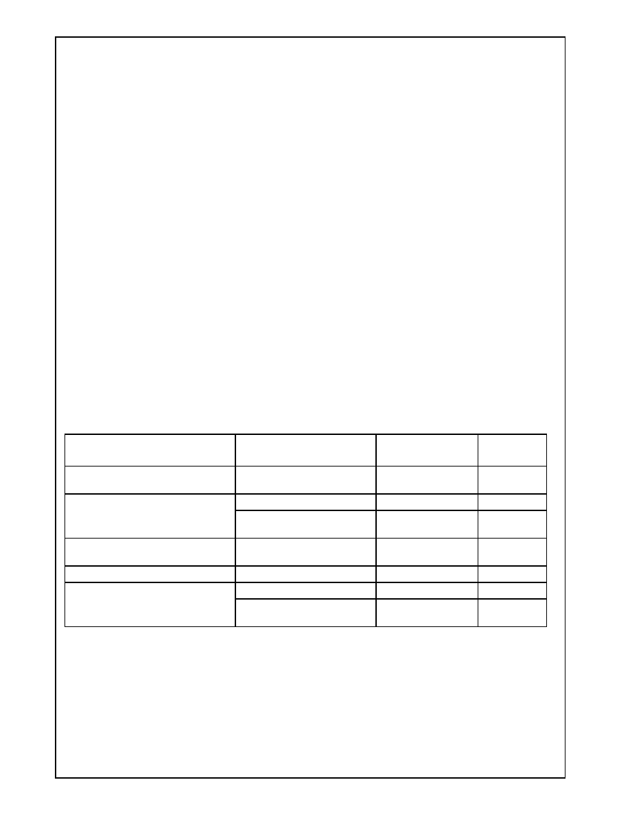
Revision 3.1
87
www.national.com
Processor Programming (
Continued
)
GeodeTM
G
Xm
P
r
ocessor
3.13.3 Privilege Level Transfers
A task's CPL can be changed only through intersegment
control transfers using gates or task switches to a code
segment with a different privilege level. Control transfers
result from exception and interrupt servicing and from
execution of the CALL, JMP, INT, IRET and RET instruc-
tions.
There are five types of control transfers that are summa-
rized in Table 3-38. Control transfers can be made only
when the operation causing the control transfer references
the correct descriptor type. Any violation of these descriptor
usage rules causes a general protection fault.
Any control transfer that changes the CPL within a task
results in a change of stack. The initial values for the stack
segment (SS) and stack pointer (ESP) for privilege levels
0, 1, and 2 are stored in the TSS. During a JMP or CALL
control transfer, the SS and ESP are loaded with the new
stack pointer and the previous stack pointer is saved on
the new stack. When returning to the original privilege
level, the RET or IRET instruction restores the SS and
ESP of the less-privileged stack.
3.13.3.1 Gates
Gate descriptors described in Section 3.7.5 "Gate
Descriptors" on page 69, provide protection for privilege
transfers among executable segments. Gates are used to
transition to routines of the same or a more privileged
level. Call gates, interrupt gates and trap gates are used for
privilege transfers within a task. Task gates are used to
transfer between tasks.
Gates conform to the standard rules of privilege. In other
words, gates can be accessed by a task if the effective
privilege level (EPL) is the same or more privileged than
the gate descriptor's privilege level (DPL).
3.13.4 Initialization and Transition to Protected Mode
The GXm processor core switches to real mode immedi-
ately after RESET. While operating in real mode, the sys-
tem tables and registers should be initialized. The GDTR
and IDTR must point to a valid GDT and IDT, respectively. The
size of the IDT should be at least 256 bytes, and the GDT
must contain descriptors that describe the initial code and
data segments.
The processor can be placed in protected mode by setting
the PE bit (CR0 register bit 0). After enabling protected
mode, the CS register should be loaded and the instruc-
tion decode queue should be flushed by executing an
intersegment JMP. Finally, all data segment registers
should be initialized with appropriate selector values.
Table 3-38. Descriptor Types Used for Control Transfer
Type of Control Transfer
Operation Types
Descriptor
Referenced
Descriptor
Table
Intersegment within the same privilege
level.
JMP, CALL, RET, IRET*
Code Segment
GDT or LDT
Intersegment to the same or a more
privileged level. Interrupt within task
(could change CPL level).
CALL
Gate Call
GDT or LDT
Interrupt Instruction, Exception,
External Interrupt
Trap or Interrupt Gate
IDT
Intersegment to a less privileged level
(changes task CPL).
RET, IRET*
Code Segment
GDT or LDT
Task Switch via TSS
CALL, JMP
Task State Segment
GDT
Task Switch via Task Gate
CALL, JMP
Task Gate
GDT or LDT
IRET**, Interrupt Instruction,
Exception, External Interrupt
Task Gate
IDT
Note:
*NT = 0 (Nested Task bit in EFLAGS, bit 14)
**NT =1 (Nested Task bit in EFLAGS, bit 14)

www.national.com
88
Revision 3.1
Processor Programming (
Continued
)
GeodeTM
G
Xm
Pr
ocessor
3.14 VIRTUAL 8086 MODE
Both real mode and virtual 8086 (V86) modes are sup-
ported by the GXm processor, allowing execution of 8086
application programs and 8086 operating systems. V86
mode allows the execution of 8086-type applications, yet
still permits use of the paging and protection mechanisms.
V86 tasks run at privilege level 3. Before entry, all seg-
ment limits must be set to FFFFh (64K) as in real mode.
3.14.1 Memory Addressing
While in V86 mode, segment registers are used in an
identical fashion to real mode. The contents of the Seg-
ment register are multiplied by 16 and added to the offset
to form the Segment Base Linear Address. The GXm pro-
cessor permits the operating system to select which pro-
grams use the V86 address mechanism and which
programs use protected mode addressing for each task.
The GXm processor also permits the use of paging when
operating in V86 mode. Using paging, the 1 MB address
space of the V86 task can be mapped to any region in the
4 GB linear address space.
The paging hardware allows multiple V86 tasks to run
concurrently, and provides protection and operating sys-
tem isolation. The paging hardware must be enabled to
run multiple V86 tasks or to relocate the address space of
a V86 task to physical address space other than 0.
3.14.2 Protection
All V86 tasks operate with the least amount of privilege
(level 3) and are subject to all CPU protected mode protec-
tion checks. As a result, any attempt to execute a privi-
leged instruction within a V86 task results in a general
protection fault.
In V86 mode, a slightly different set of instructions are
sensitive to the I/O privilege level (IOPL) than in protected
mode. These instructions are: CLI, INT n, IRET, POPF,
PUSHF, and STI. The INT3, INTO and BOUND variations
of the INT instruction are not IOPL sensitive.
3.14.3 Interrupt Handling
To fully support the emulation of an 8086-type machine,
interrupts in V86 mode are handled as follows. When an
interrupt or exception is serviced in V86 mode, program
execution transfers to the interrupt service routine at privi-
lege level 0 (i.e., transition from V86 to protected mode
occurs). The VM bit in the EFLAGS register (bit 17) is
cleared. The protected mode interrupt service routine
then determines if the interrupt came from a protected
mode or V86 application by examining the VM bit in the
EFLAGS image stored on the stack. The interrupt service
routine may then choose to allow the 8086 operating sys-
tem to handle the interrupt or may emulate the function of
the interrupt handler. Following completion of the interrupt
service routine, an IRET instruction restores the EFLAGS
register (restores VM = 1) and segment selectors and
control returns to the interrupted V86 task.
3.14.4 Entering and Leaving Virtual 8086 Mode
V86 mode is entered from protected mode by either exe-
cuting an IRET instruction at CPL = 0 or by task switching.
If an IRET is used, the stack must contain an EFLAGS
image with VM = 1. If a task switch is used, the TSS must
contain an EFLAGS image containing a 1 in the VM bit
position. The POPF instruction cannot be used to enter
V86 mode since the state of the VM bit is not affected.
V86 mode can only be exited as the result of an interrupt
or exception. The transition out must use a 32-bit trap or
interrupt gate that must point to a non-conforming privi-
lege level 0 segment (DPL = 0), or a 32-bit TSS. These
restrictions are required to permit the trap handler to IRET
back to the V86 program.

Revision 3.1
89
www.national.com
Processor Programming (
Continued
)
GeodeTM
G
Xm
P
r
ocessor
3.15 FLOATING POINT UNIT OPERATIONS
The FPU is x87-instruction-set compatible and adheres to
the IEEE-754 standard. Because most applications that
contain FPU instructions intermix with integer instructions,
the GXm processor's FPU achieves high performance by
completing integer and FPU operations in parallel.
3.15.1 FPU (Floating Point Unit) Register Set
In addition to the registers described to this point, the FPU
within the CPU provides the user eight data registers
accessed in a stack-like manner, a control register, and a
status register. The CPU also provides a data register tag
word that improves context switching and stack perfor-
mance by maintaining empty/non-empty status for each of
the eight data registers. In addition, registers contain
pointers to (a) the memory location containing the current
instruction word and (b) the memory location containing
the operand associated with the current instruction word
(if any).
3.15.2 FPU Tag Word Register
The CPU maintains a tag word register that is divided into
eight tag word fields. These fields assume one of four val-
ues depending on the contents of their associated data
registers: Valid (00), Zero (01), Special (10), and Empty
(11). Note: Denormal, Infinity, QNaN, SNaN and unsup-
ported formats are tagged as "Special". Tag values are
maintained transparently by the CPU and are only avail-
able to the programmer indirectly through the FSTENV and
FSAVE instructions. The tag word with tag fields for each
associated physical register, tag(n), is shown in Table 3-39
on page 90.
3.15.3 FPU Status Register
The FPU communicates status information and operation
results to the CPU through the status register. The fields
in the FPU status register are detailed in Table 3-39 on
page 90. These fields include information related to
exception status, operation execution status, register sta-
tus, operand class, and comparison results. This register
is continuously accessible to the CPU regardless of the
state of the Control or Execution Units.
3.15.4 FPU Mode Control Register
The FPU Mode Control Register (MCR) shown in Table 3-
39 on page 90 is used by the GXm processor to specify
the operating mode of the FPU. The MCR register fields
include information related to the rounding mode selected,
the amount of precision to be used in the calculations, and
the exception conditions which should be reported to the
GXm processor using traps. The user controls precision,
rounding, and exception reporting by setting or clearing
appropriate bits in the MCR.

www.national.com
90
Revision 3.1
Processor Programming (
Continued
)
GeodeTM
G
Xm
Pr
ocessor
Table 3-39. FPU Registers
Bit
Name
Description
FPU Tag Word Register (R/W) (Note)
15:14
TAG7
TAG7: 00 = Valid; 01 = Zero; 10 = Special; 11 = Empty.
13:12
TAG6
TAG6: 00 = Valid; 01 = Zero; 10 = Special; 11 = Empty.
11:10
TAG5
TAG5: 00 = Valid; 01 = Zero; 10 = Special; 11 = Empty.
9:8
TAG4
TAG4: 00 = Valid; 01 = Zero; 10 = Special; 11 = Empty.
7:6
TAG3
TAG3: 00 = Valid; 01 = Zero; 10 = Special; 11 = Empty.
5:4
TAG2
TAG2: 00 = Valid; 01 = Zero; 10 = Special; 11 = Empty.
3:2
TAG1
TAG1: 00 = Valid; 01 = Zero; 10 = Special; 11 = Empty.
1:0
TAG0
TAG0: 00 = Valid; 01 = Zero; 10 = Special; 11 = Empty.
FPU Status Register (R/W) (Note)
15
B
Copy of ES bit (bit 7 this register)
14
C3
Condition code bit 3
13:11
S
Top-of-Stack: Register number that points to the current TOS.
10:8
C[2:0]
Condition code bits [2:0]
7
ES
Error indicator: Set to 1 if unmasked exception detected.
6
SF
Stack Full: FPU Status Register: or invalid register operation bit.
5
P
Precision error exception bit
4
U
Underflow error exception bit
3
O
Overflow error exception bit
2
Z
Divide-by-zero exception bit
1
D
Denormalized-operand error exception bit
0
I
Invalid operation exception bit
FPU Mode Control Register (R/W) (Note)
15:12
RSVD
Reserved: Set to 0.
11:10
RC
Rounding Control Bits:
00 = Round to nearest or even
01 = Round towards minus infinity
10 = Round towards plus infinity
11 = Truncate
9:8
PC
Precision Control Bits:
00 = 24-bit mantissa
01 = Reserved
10 = 53-bit mantissa
11 = 64-bit mantissa
7:6
RSVD
Reserved: Set to 0.
5
P
Precision error exception bit
4
U
FPU Mode Control Register
3
O
Overflow error exception bit
2
Z
Divide-by-zero exception bit
1
D
Denormalized-operand error exception bit
0
I
Invalid-operation exception bit
Note: R/W only through the environment at store and restore commands.
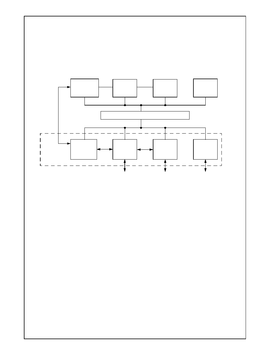
Revision 3.1
91
www.national.com
GeodeTM
G
Xm
P
r
ocessor
4.0
Integrated Functions
The Geode GXm processor integrates a memory control-
ler, graphics pipeline and display controller in a Unified
Memory Architecture (UMA). UMA simplifies system
designs and significantly reduces overall system costs
associated with high chip count, small footprint notebook
designs. Performance degradation in traditional UMA sys-
tems is reduced through the use of National Semiconduc-
tor's Display Compression Technology (DCT).
Figure 4-1 shows the major functional blocks of the GXm
processor and how the internal bus interface unit operates
as the interface between the processor's core units and
the integrated functions.
This section details how the integrated functions and inter-
nal bus interface unit operate and their respective regis-
ters.
Figure 4-1. Internal Block Diagram
Write-Back
Unit
FPU
Internal Bus Interface Unit
Graphics
Memory
Display
PCI
SDRAM Port
CS5530
PCI Bus
Integer
Cache Unit
Integrated
Functions
MMU
(CRT/LCD TFT)
X-Bus
Pipeline
Controller
Controller
Controller
C-Bus
www.national.com
92
Revision 3.1
Integrated Functions (
Continued
)
GeodeTM
G
Xm
Pr
ocessor
4.1
INTEGRATED FUNCTIONS PROGRAMMING INTERFACE
The GXm processor performs mapping for the dedicated
cache, graphics pipeline, display controller, memory con-
troller, and graphics memory, including the frame buffer. It
maps these to high memory addresses or GXm processor
memory space. The base address for these is controlled
by the Graphics Configuration Register (GCR, Index B8h),
which specifies address bits [31:30] in physical memory.
Figure 4-2 on page 93 shows the address map for the
GXm processor. When accessing the GXm processor
memory space, address bits [29:24] must be zero. This
allows the GXm processor a linear address space with a
total of 16 MB. Address bit 23 divides this space into 8 MB
for control (bit 23 = 0) and 8 MB for graphics memory (bit
23 = 1). In control space, bits [22:16] are not decoded, so
the programmer should set them to zero. Address bit 15
divides the remaining 64 KB address space into scratch-
pad RAM and PCI access (bit 15 = 0) and control regis-
ters (bit 15 = 1).
Device drivers must be responsible for performing physi-
cal-to-virtual memory-address translation, including allo-
cation of selectors that point to the GXm processor. The
processor may be accessed in protected mode by creat-
ing a selector with the physical address shown in Table 4-
1, and a limit of 16 MB. A selector with a 64 KB limit is
large enough to access all of the GXm processor's regis-
ters and scratchpad RAM.
4.1.1
Graphics Control Register
The GXm processor incorporates graphics functions that
require registers to implement and control them. Most of
these registers are memory mapped and physically
located in the logical units they control. The mapping of
these units is controlled by this configuration register. The
Graphics Control Register (GCR, Index B8h) is I/O-
mapped because it must be accessed before memory
mapping can be enabled. Refer to Section 3.3.2.2 "Con-
figuration Registers" on page 47 for information on how to
access this register.
Table 4-1. GCR Register
Bit
Name
Description
Index B8h
GCR Register (R/W)
Default Value = 00h
7:4
RSVD
Reserved: Set to 0.
3:2
SP
Scratchpad Size: Specifies the size of the scratchpad cache.
00 = 0 KB
01 = 2 KB
10 = 3 KB
11 = 4 KB
1:0
GX
GXm Base Address: Specifies the physical address for the base (GX_BASE) of the scratchpad RAM, the
graphics memory (frame buffer, compression buffer, etc.) and the other memory mapped registers.
00 = Scratchpad RAM, Graphics Subsystem, and memory-mapped configuration registers are disabled.
01 = Scratchpad RAM and control registers start at GX_BASE = 40000000h.
10 = Scratchpad RAM and control registers start at GX_BASE = 80000000h.
11 = Scratchpad RAM and control registers start at GX_BASE = C0000000h.

Revision 3.1
93
www.national.com
Integrated Functions (
Continued
)
GeodeTM
G
Xm
P
r
ocessor
Figure 4-2. GeodeTM GXm Processor Memory Space
Conventional Memory
UMBs and Expansion ROMs
Video BIOS
System BIOS
Extended Memory
PCI Access
Scratchpad
VGA/MDA
Frame Buffers
(Soft VGA and/or PCA/ISA)
Internal Bus IF Unit Registers
Graphics Pipeline Registers
SMM System Code
(Frame Buffer, etc.)
PCI Access
ROM Access
(256 KB)
0h
A0000h (640 KB)
C0000h
E0000h
100000h (1 MB)
E8000h
GX_BASE+8000h
GX_BASE+9000h
GX_BASE+400000h
GX_BASE+800000h
GX_BASE+1000000h
FFFC0000h
FFFFFFFFh (4 GB)
Extended Memory
Graphics Memory
(Frame Buffer, etc.)
0h
A0000h (640 KB)
C0000h
E0000h
100000h (1 MB)
E8000h
Shadowed Video BIOS
Shadowed System BIOS
SMM System Code
Physical Address Map
DRAM Map
MAX
*GBADD or Top of DRAM
*Top of DRAM
PCI Access
PCI Access
Display Controller Registers
Memory Controller Registers
Graphics Memory
* See BC_DRAM_TOP Table 4-10 on page 101 or MC_GBASE_ADD on page 111.
(See Table 4-29 on page 136)
(See Table 4-24 on page 124)
(See Table 4-9 on page 101)
GX_BASE (See Table
4-1 on page 92)
FFFF FFFFh
MAX
Conventional Memory
UMBs and
Expansion ROMs
GX_BASE+8500h
GX_BASE+8400h
(See Table 4-15 on page 108)
GX_BASE+8300h
GX_BASE+8100h
(See Table 4-5 on page 97)
GX_BASE+1000h
Power Management Registers
(See Table 6-1 on page 179)
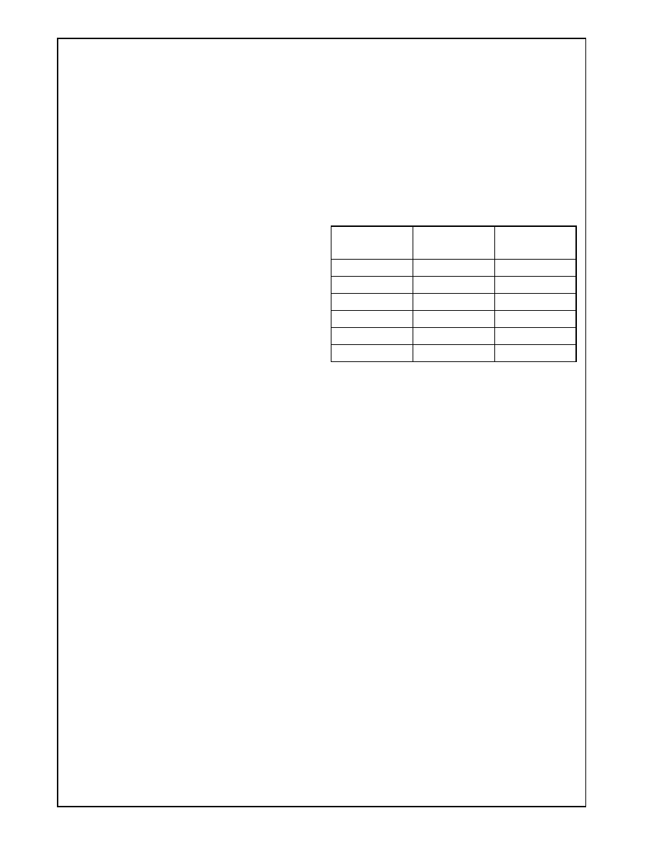
www.national.com
94
Revision 3.1
Integrated Functions (
Continued
)
GeodeTM
G
Xm
Pr
ocessor
4.1.2
Control Registers
The control registers for the GXm processor use 32 KB of
the memory map, starting at GX_BASE+8000h (see Fig-
ure 4-2 on page 93). This area is divided into internal bus
interface unit, graphics pipeline, display controller, mem-
ory controller, and power management sections:
∑ The internal bus interface unit maps 100h locations
starting at GX_BASE+8000h.
∑ The graphics pipeline maps 200h locations starting at
GX_BASE+8100h.
∑ The display controller maps 100h locations starting at
GX_BASE+8300h.
∑ The memory controller maps 100h locations starting at
GX_BASE+8400h
∑ GX_BASE+8500h-8FFFh is dedicated to power
management registers for the serial packet transmis-
sion control, the user-defined power management
address space, Suspend Refresh, and SMI status for
Suspend/Resume.
The register descriptions are contained in the individual
subsections of this chapter. Accesses to undefined regis-
ters in the GXm processor control register space will not
cause a hardware error.
4.1.3
Graphics Memory
The GXm processor's graphics memory is mapped into 8
MB starting at GX_BASE+800000h. This area includes
the frame buffer memory and storage for internal display
controller state. The frame buffer is a linear map whose
size depends on the current resolution setup in the mem-
ory controller. Frame buffer scan lines are not contiguous
in many resolutions, so software that renders to the frame
buffer must use a skip count to advance between scan
lines. The display controller uses the graphics memory
that lies between scan lines for internal state. For this rea-
son, accessing graphics memory between the end of a
scan line and the start of another can cause display prob-
lems. The skip count for all supported resolutions is
shown in Table 4-2.
Graphics memory is allocated from system DRAM by the
system BIOS. The graphics memory size is programmed
by setting the graphics memory base address in the mem-
ory controller. Display drivers communicate with system
BIOS about resolution changes, to ensure that the correct
amount of graphics memory is allocated. When a graphics
resolution change requires an increased amount of graph-
ics memory, the system must be rebooted! The reason for
this restriction is that no mechanism exists to recover sys-
tem DRAM from the operating system without rebooting.
Table 4-2. Display Resolution Skip Counts
Screen
Resolution
Pixel
Depth
Skip
Count
640x480
8 bits
1024
640x480
16 bits
2048
800x600
8 bits
1024
800x600
16 bits
2048
1024x768
8 bits
1024
1024x768
16 bits
2048

Revision 3.1
95
www.national.com
Integrated Functions (
Continued
)
GeodeTM
G
Xm
P
r
ocessor
4.1.4
L1 Cache Controller
The GXm processor contains an on-board 16 KB unified
data/instruction L1 cache. It operates in write-back mode.
Since the memory controller is also on-board, the L1
cache requires no external logic to maintain coherency. All
DMA cycles automatically snoop the L1 cache. For
improved graphics performance, part of the L1 cache
operates as a scratchpad RAM to be used by the graphics
pipeline as a BLT Buffer.
The CD bit (Cache Disable, bit 30) in CR0 globally con-
trols the operating mode of the L1 cache. LCD and LWT,
Local Cache Disable and Local Write-through bits in the
Translation Lookaside Buffer, control the mode on a page-
by-page basis. Additionally, memory configuration control
can specify certain memory regions as non-cacheable.
If the cache is disabled, no further cache line fills occur.
However, data already present in the cache continues to
be used. For the cache to be completely disabled, the
cache must be invalidated with a WBINVD instruction
after the cache has been disabled.
Write-back caching improves performance by relieving
congestion on slower external buses. With four dirty bits,
the cache marks dirty locations on a double-word basis.
This further reduces the number of double-word bus write
operations needed during a replacement or flush opera-
tion.
The GXm processor will cache SMM regions. This speeds
up system management overhead to allow for hardware
emulation such as VGA.
The cache of the GXm processor provides the ability to
redefine 2 KB, 3 KB, or 4 KB of the L1 cache to be
scratchpad memory. The scratchpad area is memory
mapped to the upper memory region defined by the GCR
register (Index B8h). The valid bits for the scratchpad
RAM will always be true and the scratchpad RAM loca-
tions will never be flushed to memory. The scratchpad
RAM serves as a general purpose high speed RAM and
as a BLT buffer for the graphics pipeline. Incrementing
BLT buffer address registers have been added to enable
the graphics pipeline to access this memory as a BLT
buffer. A 16-byte line buffer dedicated to the graphics
pipeline accesses has been added to minimize graphics
interference with normal CPU operation.
Table 4-3 summarizes the registers contained in the L1
cache. These registers do not have default values and
must be initialized before use. Table 4-4 on page 96 gives
the register/bit formats.
Table 4-3. L1 Cache BitBLT Register Summary
Mnemonic Name
Function
L1_BB0_BASE
L1 Cache BitBLT 0 Base Address
Contains the address offset to the first byte of BLT Buffer 0 in the scratch-
pad memory.
L1_BB0_POINTER
L1 Cache BitBLT 0 Pointer
Contains the address offset to the current line of BLT Buffer 0 in the
scratchpad memory.
L1_BB1_BASE
L1 Cache BitBLT 1 Base Address
Contains the offset to the first byte of BLT Buffer 1 in the scratchpad mem-
ory.
L1_BB1_POINTER
L1 Cache BitBLT 1 Pointer
Contains the address offset to the current line of BLT Buffer 1 in the
scratchpad memory.
Note:
For information on accessing these registers, refer to Section 4.1.6 "CPU_READ/CPU_WRITE Instructions"
on page 99.
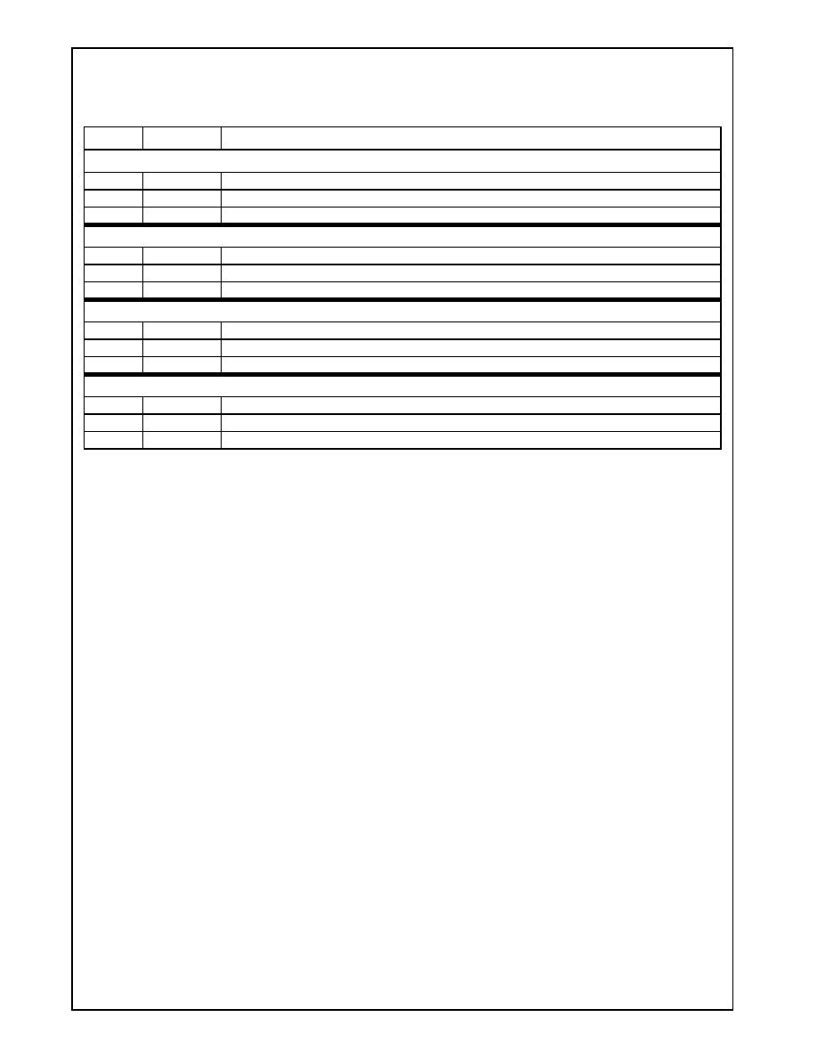
www.national.com
96
Revision 3.1
Integrated Functions (
Continued
)
GeodeTM
G
Xm
Pr
ocessor
Table 4-4. L1 Cache BitBLT Registers
Bit
Name
Description
L1_BB0_BASE Register (R/W)
Default Value = None
15:12
RSVD
Reserved: Set to 0.
11:4
INDEX
BitBLT 0 Base Index: The index to the starting line of BLT Buffer 0.
3:0
BYTE
BitBLT 0 Starting Byte: Determines which byte of the starting line is the beginning of BLT Buffer 0.
L1_BB0_POINTER Register (R/W)
Default Value = None
15:12
RSVD
Reserved: Set to 0.
11:4
INDEX
BitBLT 0 Pointer Index: The index to the current line of BLT Buffer 0.
3:0
RSVD
Reserved: Set to 0.
L1_BB1_Base Register (R/W)
Default Value = None
15:12
RSVD
Reserved: Set to 0.
11:4
INDEX
BitBLT 1 Base Index: The index to the starting line of BLT Buffer 1.
3:0
BYTE
BitBLT 1 Starting Byte: Determines which byte of the starting line is the beginning of BLT Buffer 1.
L1_BB1_POINTER Register (R/W)
Default Value = None
15:12
RSVD
Reserved: Set to 0.
11:4
INDEX
BitBLT 1 Pointer Index: The index to the current line of BLT Buffer 1.
3:0
RSVD
Reserved: Set to 0.
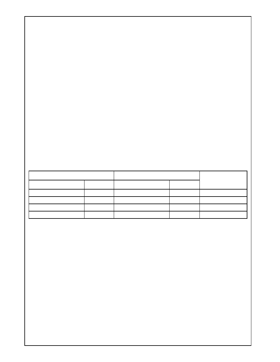
Revision 3.1
97
www.national.com
Integrated Functions (
Continued
)
GeodeTM
G
Xm
P
r
ocessor
4.1.4.1
Scratchpad Memory
The scratchpad RAM is a dedicated high-speed memory
cache that contains BLT buffers, SMM header, and a
scratchpad area for display drivers. It provides both L1
cache performance and a dedicated resource that cannot
be thrown out by other system activity. The configuration
of the scratchpad is based on graphics resolution and is
described in Table 4-5.
The scratchpad memory is part of the on-chip L1 cache
memory. The memory size is controlled by bits in the GCR
register (Index B8h). The scratchpad memory can be dis-
abled, or sized to 2 KB, 3 KB, or 4 KB. The remaining L1
cache size is 16 KB minus the scratchpad size, and all of
the scratchpad area is subtracted from a single way.
The scratchpad memory is used by display drivers and
virtualization software. Because this resource must be
tightly controlled to avoid conflicts, application software
and third-party drivers should avoid accesses to the
scratchpad area.
The display driver creates and manages two BLT buffers
from within the scratchpad area. These BLT buffers are
used to transfer source data from system memory into the
frame buffer, or for destination data from system memory
or the frame buffer. The graphics pipeline accesses the
BLT buffers for many common operations, including Bit-
BLT transfers, output primitives, and raster text. Display
drivers also use a small portion of the scratchpad as an
extended register file, since scratchpad read and write
accesses are very fast compared to normal memory oper-
ations.
The virtualization software uses the scratchpad area to
store critical SMM information, including the SMI header
and SMM system state. No SMM code currently resides in
the scratchpad area, although this is an option for future
products.
When the BLT buffer pointer is used (refer to Table 4-8 on
page 99) addresses outside the scratchpad range will
wrap around back into the scratchpad RAM. Table 4-5
shows the allocation of scratchpad memory for the 2 KB
and 3 KB configurations of the scratchpad. The 2 KB con-
figuration uses GX_BASE+0800h to GX_BASE+1000h.
The 3 KB configuration uses GX_BASE+0400h to
GX_BASE+1000h. These configurations are fixed by the
system BIOS during boot and cannot be changed without
rebooting the system.
Table 4-5. Scratchpad Organization
2 KB Configuration
3 KB Configuration
Description
Offset
Size
Offset
Size
GX_BASE + 0EE0h
288 bytes
GX_BASE + 0EE0h
288 bytes
SMM scratchpad
GX_BASE + 0E60h
128 bytes
GX_BASE + 0E60h
128 bytes
Driver scratchpad
GX_BASE + 0B30h
816 bytes
GX_BASE + 0930h
1328 bytes
BLT Buffer 0
GX_BASE + 0800h
816 bytes
GX_BASE + 0400h
1328 bytes
BLT Buffer 1

www.national.com
98
Revision 3.1
Integrated Functions (
Continued
)
GeodeTM
G
Xm
Pr
ocessor
4.1.5
Display Driver Instructions
The GXm processor has four instructions to access pro-
cessor core registers. Table 4-6 shows these instructions.
Adding CPU instructions does not create a compatibility
problem for applications that may depend on receiving
illegal opcode traps. The solution is to make these instruc-
tions generate an illegal opcode trap unless a compatibil-
ity bit is explicitly set. The GXm processor uses the
scratchpad size field (bits [3:2] in GCR, Index B8h) to
enable or disable all of the graphics instructions. If the
scratchpad size bits are zero, meaning that none of the
cache is defined as scratchpad, then hardware will
assume that the graphics controller is not being used and
the graphics instructions will be disabled. Any other
scratchpad size will enable all of the new instructions.
Note that the base address of the memory map in the
GCR register can still be set up to allow access to the
memory controller registers.
Table 4-6. Display Driver Instructions
Syntax
Opcode
Description
BB0_RESET
0F3A
Reset the BLT Buffer 0 pointer to the base.
BB1_RESET
0F3B
Reset the BLT Buffer 1 pointer to the base.
CPU_WRITE
0F3C
Write data to CPU internal register.
CPU_READ
0F3D
Read data from CPU internal register.
Revision 3.1
99
www.national.com
Integrated Functions (
Continued
)
GeodeTM
G
Xm
P
r
ocessor
4.1.6
CPU_READ/CPU_WRITE Instructions
The GXm processor has several internal registers that
control the BLT buffer and power management circuitry in
the dedicated cache subsystem. To avoid adding addi-
tional instructions to read and write these registers, the
GXm processor has a general mechanism to access inter-
nal CPU registers with reasonable performance. The
GXm processor has two special instructions to read and
write CPU registers: CPU_READ and CPU_WRITE. Both
instructions fetch a 32-bit register address from EBX as
shown in Table 4-7 and Table 4-8. CPU_WRITE uses EAX
for the source data, and CPU_READ uses EAX as the
destination. Both instructions always transfer 32 bits of
data.
These instructions work by initiating a special I/O transac-
tion where the high address bit is set. This provides a very
large address space for internal CPU registers.
The BLT buffer base registers define the starting physical
addresses of the BLT buffers located within the dedicated
L1 cache. The dedicated cache can be configured for up
to 4 KB, so 12 address bits are required for each base
address.
Table 4-7. CPU-Access Instructions
Syntax
Opcode
Registers
Length
CPU_WRITE
0F3Ch
EBX = 32-bit address, EAX = Source
2 bytes
CPU_READ
0F3Dh
EBX = 32-bit address, EAX = Destination
2 bytes
Table 4-8. Address Map for CPU-Access Registers
Register
EBX Address
Description
L1_BB0_BASE
FFFFFF0Ch
BLT Buffer 0 base address (see Table 4-4 on page 96).
L1_BB1_BASE
FFFFFF1Ch
BLT Buffer 1 base address (see Table 4-4 on page 96).
L1_BB0_POINTER
FFFFFF2Ch
BLT Buffer 0 pointer address (see Table 4-4 on page 96).
L1_BB1_POINTER
FFFFFF3Ch
BLT Buffer 1 pointer address (see Table 4-4 on page 96).
PM_BASE
FFFFFF6Ch
Power management base address (see Table 6-3 on page 181).
PM_MASK
FFFFFF7Ch
Power management address mask (see Table 6-3 on page 181).

www.national.com
100
Revision 3.1
Integrated Functions (
Continued
)
GeodeTM
G
Xm
Pr
ocessor
4.2
INTERNAL BUS INTERFACE UNIT
The Geode GXm processor's internal bus interface unit
provides control and interface functions to the internal C-
Bus (processor core, FPU, graphics pipeline, and L1
cache) and X-Bus (PCI controller, display controller, mem-
ory controller, and graphics accelerator) paths, provides
control for several sections of memory, and plays an
important part in the virtual VGA function.
The internal bus interface unit performs, without loss of
compatibility, the functions that previously required the
external pins IGNNE# and A20M#.
The internal bus interface unit provides configuration con-
trol for up to 20 different regions within system memory. It
provides 19 configurable memory regions in the address
space between 640 KB and 1 MB, with separate control
for read access, write access, cacheability, and PCI
access.
The memory configuration control includes a top-of-mem-
ory register and hardware support for VGA emulation
plus, the capability to program 20 regions of the memory
map for different ROM configurations, and to locate mem-
ory-mapped I/O.
4.2.1
FPU Error Support
The FERR# (floating point error) and IGNNE# (ignore
numeric error) pins of the 486 microprocessor have been
replaced with an IRQ13 (interrupt request 13) pin. In DOS
systems, FPU errors are reported by the external vector
13. This mode of operation is specified by clearing the NE
bit (bit 5) in the CR0 register. If the NE bit is active, the
IRQ13 output of the GXm processor is always driven inac-
tive. If the NE bit is cleared, the GXm processor drives
IRQ13 active when the ES bit (bit 7) in the FPU Status
Register is set high. Software must respond to this inter-
rupt with an OUT instruction of an 8-bit operand to F0h or
F1h. When the OUT cycle occurs, the IRQ13 pin is driven
inactive and the FPU starts ignoring numeric errors. When
the ES bit is cleared, the FPU resumes monitoring
numeric errors.
4.2.2
A20M Support
The GXm processor provides an A20M bit in the
BC_XMAP_1 Register (GX_BASE+ 8004h[21]) to replace
the A20M# pin on the 486 microprocessor. When the
A20M bit is set high, all non-SMI accesses will have
address bit 20 forced to zero. External hardware must do
an SMI trap on I/O locations that toggle the A20M# pin.
The SMI software can then change the A20M bit as
desired.
This maintains compatibility with software that depends
on wrapping the address at bit 20.
4.2.3
SMI Generation
The internal bus interface unit can generate SMI inter-
rupts whenever an I/O cycle in the VGA address range is
3B0h-3BFh and 3C0h-3CFh. An I/O cycle to 3D0h-3DFh
can be trapped. In case an external VGA card is present,
the Internal Bus Interface Unit default values will not gen-
erate an interrupt on VGA accesses. (Refer to Section
5.2.3.1 "SMI Generation" on page 168 for instructions on
how to configure the registers to generate the SMI inter-
rupt.)
4.2.4
640 KB to 1 MB Region
There are 19 configurable memory regions located
between 640 KB and 1 MB. Three of the regions are
A0000h-AFFFFh,
B0000h-B7FFFh,
and
B8000h-
BFFFFh. The area between C0000h and FFFFFh is
divided into 16 KB segments to form the remaining 16
regions. Each of these regions has four control bits to
allow any combination of read-access, write-access,
cache, and PCI-access capabilities (Table 4-11 on page
102).
In addition, each of the three regions defined in the
A0000h-BFFFh area of memory has a VGA control bit that
can cause the graphics pipeline to handle accesses to
that section of memory (see Table 5-3 on page 170).
Revision 3.1
101
www.national.com
Integrated Functions (
Continued
)
GeodeTM
G
Xm
P
r
ocessor
4.2.5
Internal Bus Interface Unit Registers
The Internal Bus Interface Unit maps 100h locations start-
ing at GX_BASE+8000h. Refer to Section 4.1.2 "Control
Registers" on page 94 for instructions on accessing these
registers.
Table 4-9 summarizes the four 32-bit registers contained
in the Internal Bus Interface Unit and Table 4-10 gives the
register/bit formats.
Table 4-9. Internal Bus Interface Unit Register Summary
GX_BASE+
Memory Offset
Type
Name/Function
Default
Value
8000h-8003h
R/W
BC_DRAM_TOP
Top of DRAM: Contains the highest available address of system memory not
including the memory that is set aside for graphics memory, which corresponds to
1 GByte of memory. The largest possible value for the register is 3FFFFFFFh.
3FFFFFFFh
8004h-8007h
R/W
BC_XMAP_1
Memory X-Bus Map Register 1 (A and B Region Control: Contains the region
control of the A and B regions and the SMI controls required for VGA emulation.
PCI access to internal registers and the A20M function are also controlled by this
register.
00000000h
8008h-800Bh
R/W
BC_XMAP_2
Memory X-Bus Map Register 2 (C and D Region Control): Contains region con-
trol fields for eight regions in the address range C0h through DCh.
00000000h
800Ch-800Fh
R/W
BC_XMAP_3
Memory X-Bus Map Register 3 (E and F Region Control): Contains the region
control fields for memory regions in the address range E0h through FCh.
00000000h
Table 4-10. Internal Bus Interface Unit Registers
Bit
Name
Description
GX_BASE+8000h-8003h
BC_DRAM_TOP Register (R/W)
Default Value = 3FFFFFFFh
31:30
RSVD
Reserved: Set to 0.
29:17
TOP OF
DRAM
Top of DRAM: Maximum value is FFFh.
16:0
1FFFF
Granularity: Must be set to 1FFFFh (128 KB).
GX_BASE+8004h-8007h
BC_XMAP_1 Register (R/W)
Default Value = 00000000h
31:29
RSVD
Reserved: Set to 0.
28
GEB8
Graphics Enable for B8 Region: Allow memory R/W operations for address range B8000h-BFFFFh be
directed to the graphics pipeline: 0 = Disable; 1 = Enable.
(Used for VGA emulation.)
27:24
B8
B8 Region: Region control field for address range B8000h-BFFFFh.
Note: Refer to Table 4-11 for decode.
23
RSVD
Reserved: Set to 0.
22
PRAE
PCI Register Access Enable: Allow PCI Slave to access internal registers on the X-Bus:
0 = Disable; 1 = Enable.
21
A20M
Address Bit 20 Mask: Address bit 20 is always forced to a zero except for SMI accesses:
0 = Disable; 1 = Enable.
20
GEB0
Graphics Enable for B0 Region: Allow memory R/W operations for address range B0000h-B7FFFh be
directed to the graphics pipeline: 0 = Disable; 1 = Enable.
(Used for VGA emulation.)
19:16
B0
B0 Region: Region control field for address range B0000h-B7FFFh.
Note: Refer to Table 4-11 for decode.
15
SMID
SMID: All I/O accesses for address range 3D0h-3DFh generate an SMI: 0 = Disable; 1 = Enable.
(Used for VGA virtualization.)
14
SMIC
SMIC: All I/O accesses for address range 3C0h-3CFh generate an SMI: 0 = Disable; 1 = Enable.
(Used for VGA virtualization.)
13
SMIB
SMIB: All I/O accesses for address range 3B0h-3BFh generate an SMI: 0 = Disable; 1 = Enable
(Used for VGA virtualization.)
www.national.com
102
Revision 3.1
Integrated Functions (
Continued
)
GeodeTM
G
Xm
Pr
ocessor
12:8
RSVD
Reserved: Set to 0.
7
XPD
X-Bus Pipeline Disable: When cleared, the address for the next cycle can be driven on the internal X-
Bus before the completion of the data phase of the current cycle.
6
GNWS
X-Bus Graphics Pipe No Wait State: Data driven on X-Bus from graphics pipeline:
0 = 1 full clock before X_DSX is asserted
1 = On the same clock in which X_RDY is asserted
5
XNWS
X-Bus No Wait State: Data driven on X-Bus from Internal Bus Interface Unit:
0 = 1 full clock before X_DSX is asserted
1 = On the same clock in which X_RDY is asserted
4
GEA
Graphics Enable for A Region: Memory R/W operations for address range A0000h-AFFFFh are
directed to the graphics pipeline: 0 = Disable; 1 = Enable.
(Used for VGA emulation.)
3:0
A0
A0 Region: Region control field for address range A0000h-AFFFFh.
Note: Refer to Table 4-11 for decode.
GX_BASE+8008h-800Bh
BC_XMAP_2 Register (R/W)
Default Value = 00000000h
31:28
DC
DC Region: Region control field for address range DC000h to DFFFFh.
27:24
D8
D8 Region: Region control field for address range D8000h to DBFFFh.
23:20
D4
D4 Region: Region control field for address range D4000h to D7FFFh.
19:16
D0
D0 Region: Region control field for address range D0000h to D3FFFh.
15:12
CC
CC Region: Region control field for address range CC000h to CFFFFh.
11:8
C8
C8 Region: Region control field for address range C8000h to CBFFF.
7:4
C4
C4 Region: Region control field for address range C4000h to C7FFFh.
3:0
C0
C0 Region: Region control field for address range C0000h to C3FFFh.
Note: Refer to Table 4-11 for decode.
GX_BASE+800Ch-800Fh
BC_XMAP_3 Register (R/W)
Default Value = 00000000h
31:28
FC
FC Region: Region control field for address range FC000h to FFFFFh.
27:24
F8
F8 Region: Region control field for address range F8000h to FBFFFh.
23:20
F4
F4 Region: Region control field for address range F4000h to F7FFFh.
19:16
F0
F0 Region: Region control field for address range F0000h to F3FFFh.
15:12
EC
EC Region: Region control field for address range EC000h to EFFFFh.
11:8
E8
E8 Region: Region control field for address range E8000h to EBFFFh.
7:4
E4
E4 Region: Region control field for address range E4000h to E7FFFh.
3:0
E0
E0 Region: Region control field for address range E0000h to E3FFFh.
Note: Refer to Table 4-11 for decode.
Table 4-10. Internal Bus Interface Unit Registers (Continued)
Bit
Name
Description
Table 4-11. Region-Control-Field Bit Definitions
Bit
Position
Function
3
PCI Accessible: The PCI slave can access this memory if this bit is set high and if the appropriate Read or Write Enable
bit is also set high.
2
Cache Enable: Caching this region of memory is inhibited if this bit is cleared.
1
Write Enable: Write operations to this region of memory are allowed if this bit is set high. If this bit is cleared, then write
operations in this region are directed to the PCI master.
0
Read Enable: Read operations to this region of memory are allowed if this bit is set high. If this bit is cleared then read
operations in this region are directed to the PCI master.
Note: If Cache Enable = 1 and Write Enable = 1, the Write Enable determination occurs after the data has passed the cache. Since
the cache does write update, write data will change the cache if the address is cached. If a read then occurs to that address.
the data will come from the written data that is in the cache even though the address is not writable. If this must be avoided
then do not make the region cacheable.
Revision 3.1
103
www.national.com
Integrated Functions (
Continued
)
GeodeTM
G
Xm
P
r
ocessor
4.3
MEMORY CONTROLLER
The memory controller operates with the Processor Inter-
face (X-Bus), Display Controller Interface, Graphics Pipe-
line Interface, and the SDRAM Interface.
The GXm processor supports LVTTL (low voltage TTL)
technology. LVTTL technology allows the SDRAM inter-
face of the memory controller to run at frequencies up to
100 MHz.
The SDRAM clock is a function of the core clock. The
SDRAM bus can be run at speeds that range between 66
MHz and 100 MHz. The core clock can be divided down
from two to five in half clock increments to generate the
SDRAM clock. SDRAM frequencies between 79 MHz and
100 MHz are only supported for certain types of closed
systems and strict design rules must be adhered to. For
further details, please contact your local National Semi-
conductor technical support representative.
A basic block diagram of the memory controller is shown
in Figure 4-3.
Figure 4-3. Memory Controller Block Diagram
Address
Processor/PCI
Display Controller
Graphics Pipeline
Processor/PCI Address
Processor I/F
Display Controller I/F
Graphics Pipeline I/F
Arbiter
SDRAM
RASA#,RASB#
CKEA#, CKEB#
WEA#/WEB#
Configuration
MA[12:0]
BA[1:0]
Display Controller Address
Graphics Pipeline Address
Processor/PCI Data
Display Controller Data
Graphics Pipeline Data
Processor/PCI
Display Controller
MD[63:0]
Read Buffer
(16 Bytes)
Sequence
Controller
Timing
Controller
Registers
Control/MUX
Write Buffer (16 Bytes)
Write Buffer (16 Bytes)
Graphics Controller
Write Buffer (16 Bytes)
Control
Control
Control
DQM[7:0]
CASA#,CASB#
CS[3:0]#
REF
Clock Divider
2, 2.5, 3, 3.5, 4
SDCLK[3:0]
Core Clock (ph2)
www.national.com
104
Revision 3.1
Integrated Functions (
Continued
)
GeodeTM
G
Xm
Pr
ocessor
4.3.1
Memory Array Configuration
The memory controller supports up to two 64-bit, 168-pin
unbuffered
SDRAM
modules
(DIMM).
Each
DIMM
receives a unique set of RAS, CAS, WE, and CKE lines.
Each DIMM can have one or two 64-bit DIMM banks.
Each DIMM bank is selected by a unique chip select (CS).
There are four chip select signals to choose between a
total of four DIMM banks. Each DIMM bank also receives
a unique SDCLK. Each DIMM bank can have two or four
component banks. Component bank selection is done
through the bank address (BA) lines.
For example, 16 Mb SDRAMS have two component
banks and 64 Mb SDRAMs have two or four component
banks. For single DIMM bank modules, the memory con-
troller can support two DIMMS with a maximum of eight
component banks. For dual DIMM bank modules, the
memory controller can support two DIMMs with a maxi-
mum of 16 component banks. Up to 16 banks can be
open at the same time.
Figure 4-4. Memory Array Configuration
MA[12:0]
BA[1:0]
MD[63:0]
DQM[7:0]
RASA#
CASA#
WEA#
CS1#
CS0#
CKEA
SDCLK0
SDCLK1
RASB#
CASB#
WEB#
CS3#
CS2#
CKEB
SDCLK2
SDCLK3
A[12:0]
BA[1:0]
MD[63:0]
DQM[7:0]
RAS#
CAS#
WE#
S0#, S2#
CKE0
CK0, CK2
A[12:0]
BA[1:0]
MD[63:0]
DQM[7:0]
RAS#
CAS#
WE#
S1#, S3#
CKE1
CK1, CK3
Bank 0
Bank 1
A[12:0]
BA[1:0]
MD[63:0]
DQM[7:0]
RAS#
CAS#
WE#
S0#, S2#
CKE0
CK0, CK2
A[12:0]
BA[1:0]
MD[63:0]
DQM[7:0]
RAS#
CAS#
WE#
S1#, S3#
CKE1
CK1, CK3
Bank 0
Bank 1
DIMM 1
DIMM 0
GeodeTM GXm
Processor
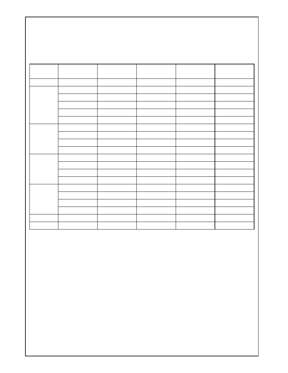
Revision 3.1
105
www.national.com
Integrated Functions (
Continued
)
GeodeTM
G
Xm
P
r
ocessor
4.3.2
Memory Organizations
The memory controller supports JEDEC standard synchronous DRAMs in 16 Mb and 64 Mb configurations. Supported
configurations are shown in Table 4-12.
Table 4-12. Synchronous DRAM Configurations
Depth
Organization
Row
Address
Column Address
Bank
Address
Total # of
Address bits
1
1 Mx16
A10-A0
A7-A0
BA0
20
2
2 Mx8
A10-A0
A8-A0
BA0
21
2 Mx32
A10-A0
A7-A0
BA1-BA0
21
2 Mx32
A10-A0
A8-A0
BA0
21
2 Mx32
A11-A0
A6-A0
BA1-BA0
21
2 Mx32
A12-A0
A6-A0
BA0
21
4
4 Mx4
A10-A0
A9-A0
BA0
22
4 Mx16
A11-A0
A7-A0
BA1-BA0
22
4 Mx16
A12-A0
A7-A0
BA0
22
4 Mx16
A10-A0
A9-A0
BA0
22
8
8 Mx8
A11-A0
A8-A0
BA1-BA0
23
8 Mx8
A12-A0
A8-A0
BA0
23
8 Mx32
A11-A0
A8-A0
BA1-BA0
23
8 Mx32
A12-A0
A7-A0
BA1-BA0
23
16
16 Mx4
A11-A0
A9-A0
BA1-BA0
24
16 Mx4
A12-A0
A9-A0
BA0
24
16 Mx16
A12-A0
A8-A0
BA1-BA0
24
16 Mx16
A11-A0
A9-A0
BA1-BA0
24
32
32 Mx8
A12-A0
A9-A0
BA1-BA0
25
64
64 Mx4
A12-A0
A9-A0,A11
BA1-BA0
26
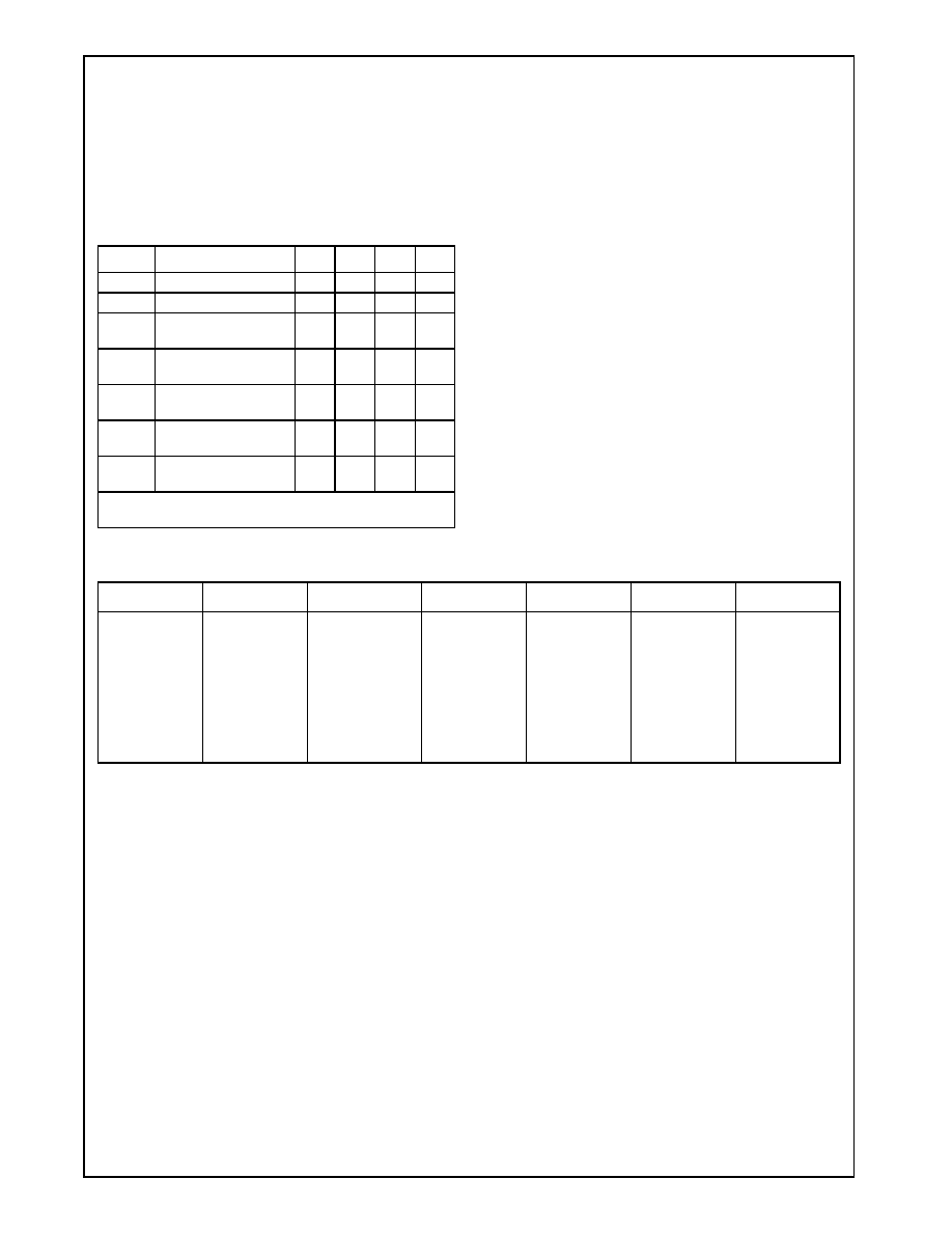
www.national.com
106
Revision 3.1
Integrated Functions (
Continued
)
GeodeTM
G
Xm
Pr
ocessor
4.3.3
SDRAM Commands
This subsection discusses the SDRAM commands sup-
ported by the memory controller. Table 4-13 summarizes
these commands followed by detailed operational infor-
mation regarding each command.
MRS -- The Mode Register command defines the specific
mode of operation of the SDRAM. This definition includes
the selection of burst length, burst type, and CAS latency.
CAS latency is the delay, in clock cycles, between the reg-
istration of a read command and the availability of the first
piece of output data.
The burst length is programmed by address bits MA[2:0],
the burst type by address bit MA3 and the CAS latency by
address bits MA[6:4].
The memory controller only supports a burst length of two
and burst type of interleave.
The field value on MA[12:0] and BA[1:0] during the MRS
cycle are as shown in Table 4-14.
PRE -- The precharge command is used to deactivate
the open row in a particular bank or the open row in both
component banks. Address pin MA10 determines whether
one or both banks are to be precharged. In the case
where only one component bank is to be precharged,
BA[1:0] selects which bank. Once a bank has been pre-
charged, it is in the Idle state and must be activated prior
to any read or write commands.
Table 4-13. Basic Command Truth Table
Name
Command
CS
RAS
CAS
WE
MRS
Mode Register Set
L
L
L
L
PRE
Bank Precharge
L
L
H
L
ACT
Bank activate/row-
address entry
L
L
H
H
WRT
Column address
entry/Write operation
L
H
L
L
READ
Column address
entry/Read operation
L
H
L
H
DESL
Control input inhibit/
No operation
H
X
X
X
REFR*
CBR Refresh or Auto
Refresh
L
L
L
H
Note: *This command is CBR (CAS-before-RAS) refresh
when CKE is high and self refresh when CKE is low.
Table 4-14. Address Line Programming during MRS Cycles
BA[1:0]
MA[12:7]
MA[6:4]
MA3
MA2
MA1
MA0
00
000000
CAS Latency:
000 = Reserved
010 = 2 CLK
100 = 4 CLK
110 = 6 CLK
001 = 1 CLK
011 = 3 CLK
101 = 5 CLK
111 = 7 CLK
1
0
0
1

Revision 3.1
107
www.national.com
Integrated Functions (
Continued
)
GeodeTM
G
Xm
P
r
ocessor
ACT -- The activate command is used to open a row in a
particular bank for a subsequent access. The value on the
BA lines selects the bank, and the address on the MA
lines selects the row. This row remains open for accesses
until a precharge command is issued to that bank. A pre-
charge command must be issued before opening a differ-
ent row in the same bank.
READ -- The read command is used to initiate a burst
read access to an active row. The value on the BA lines
select the component bank, and the address provided by
the MA lines select the starting column location. The
memory controller does not perform auto precharge dur-
ing read operations. Valid data-out from the starting col-
umn address is available following the CAS latency after
the read command. The DQM signals are asserted low
during read operations.
WRT -- The write command is used to initiate a burst
write access to an active row. The value on the BA liens
select the component bank, and the address provided by
the MA lines select the starting column location. The
memory controller does not perform auto precharge dur-
ing write operations. This leaves the page open for subse-
quent accesses. Data appearing on the MD lines is
written to the DQM logic level appearing coincident with
the data. If the DQM signal is registered low, the corre-
sponding data will be written to memory. If the DQM is
driven high, the corresponding data will be ignored, and a
write will not be executed to that location.
REF -- Auto refresh is used during normal operation and
is analogous to the CAS-before-RAS (CBR) refresh in
conventional DRAMs.During auto refresh the address bits
are "don't care". The memory controller precharges all
banks prior to an auto refresh cycle. Auto refresh cycles
are issued approximately 15 µs apart.
The self refresh command is used to retain data in the
SDRAMs even when the rest of the system is powered
down. The self refresh command is similar to an auto
refresh command except CKE is disabled (low). The
memory controller issues a self refresh command during
3V Suspend mode when all the internal clocks are
stopped.
4.3.3.1
SDRAM Initialization Sequence
After the clocks have started and stabilized, the memory
controller SDRAM initialization sequence begins:
1)
Precharge all component banks
2)
Perform eight refresh cycles
3)
Perform an MRS cycle
4)
Perform eight refresh cycles
This sequence is compatible with the majority of SDRAMs
available from the various vendors.
www.national.com
108
Revision 3.1
Integrated Functions (
Continued
)
GeodeTM
G
Xm
Pr
ocessor
4.3.4
Memory Controller Register Description
The Memory Controller maps 100h locations starting at
GX_BASE+8400h. Refer to Section 4.1.2 "Control Regis-
ters" on page 94 for instructions on accessing these regis-
ters.
Table 4-15 summarizes the 32-bit registers contained in
the memory controller. Table 4-16 gives detailed regis-
ter/bit formats.
Table 4-15. Memory Controller Register Summary
GX_BASE+
Memory Offset
Type
Name/Function
Default Value
8400h-8403h
R/W
MC_MEM_CNTRL1
Memory Controller Control Register 1: Memory controller configuration informa-
tion e.g., refresh interval, SDCLK ratio, etc.
248C0040h
8404h-8407h
R/W
MC_MEM_CNTRL2
Memory Controller Control Register 2: Memory controller configuration informa-
tion to control SDCLK.
00000801h
8408h-840Bh
R/W
MC_BANK_CFG
Memory Controller Bank Configuration: Contains the configuration information for
the each of the two DIMMs in the memory array. BIOS programs this register dur-
ing boot by running an autosizing routine on the memory.
41104110h
840Ch-840Fh
R/W
MC_SYNC_TIM1
Memory Controller Synchronous Timing Register 1: SDRAM memory timing
information - This register controls the memory timing of all four banks of DRAM.
BIOS programs this register based on the processor frequency and the SDCLK
divide ratio.
2A733225h
8414h-8417h
R/W
MC_GBASE_ADD
Memory Controller Graphics Base Address Register: This register sets the
graphics memory base address, which is programmable on 512 KB boundaries.
The display controller and the graphics pipeline generate a 20-bit DWORD offset
that is added to the graphics memory base address to form the physical memory
address. Typically, the graphics memory region is located at the top of physical
memory.
00000000h
8418h-841Bh
R/W
MC_DR_ADD
Memory Controller Dirty RAM Address Register: This register is used to set the
Dirty RAM address index for processor diagnostic access. This register should be
initialized before accessing the MC_DR_ACC register
00000000h
841Ch-841Fh
R/W
MC_DR_ACC
Memory Controller Dirty RAM Access Register: This register is used to access
the Dirty RAM. A read/write to this register will access the Dirty RAM at the
address specified in the MC_DR_ADD register.
0000000xh
Table 4-16. Memory Controller Registers
Bit
Name
Description
GX_BASE+ 8400h-8403h
MC_MEM_CNTRL1 (R/W)
Default Value = 248C0040h
31:29
MDHDCTL
MD High Drive Control: Controls the high drive and slew rate of the memory data bus (MD[63:0]):
000 = Tristate
001 = Smallest drive strength
010 -110 = Represents gradual drive strength increase
111 = Highest drive strength
28:26
MABAHDCTL
MA/BA High Drive Control: Controls the high drive and slew rate of the memory address bus includ-
ing the memory bank address bus (MA[12:0] and BA[1:0]):
000 = Tristate
001 = Smallest drive strength
010 -110 = Represents gradual drive strength increase
111 = Highest drive strength

Revision 3.1
109
www.national.com
Integrated Functions (
Continued
)
GeodeTM
G
Xm
P
r
ocessor
25:23
MEMHDCTL
Control High Drive/Slew Control: Controls the high drive and slew rate of the memory control sig-
nals (CASA#, CASB#, RASA#, RASB#, CKEA, CKEB, WEA#, WEA#, DQM[7:0], and CS[3:0]#):
000 = Tristate
001 = Smallest drive strength
010 -110 = Represents gradual drive strength increase
111 = Highest drive strength
22
RSVD
Reserved: Set to 0.
21
RSVD
Reserved: Must be set to 0. Wait state on the X-Bus x_data during read cycles - for debug only.
20:18
SDCLKRATE
SDRAM Clock Ratio: Selects SDRAM clock ratio:
000 = Reserved
100 = ˜ 3.5
001 = ˜ 2
101 = ˜ 4
010 = ˜ 2.5
110 = ˜ 4.5
011 = ˜ 3 (Default)
111 = ˜ 5
Ratio does not take effect until the SDCLKSTRT bit (bit 17 of this register) transitions from 0 to 1.
17
SDCLKSTRT
Start SDCLK: Start operating SDCLK using the new ratio and shift value (selected in bits [20:18] of
this register): 0 = Clear; 1 = Enable.
This bit should be cleared every time before a one is written to it in order to start SDCLK or to change
the shift value.
16:8
RFSHRATE
Refresh Interval: This field determines the number of processor core clocks multiplied by 64 between
refresh cycles to the DRAM. By default, the refresh interval is 00h. This implies that refresh is turned
off by default.
7:6
RFSHSTAG
Refresh Staggering: This field determines number of clocks between REF commands to different
banks during refresh cycles:
00 = 0 SDRAM clocks
10 = 2 SDRAM clocks
01 = 1 SDRAM clocks (Default)
11 = 4 SDRAM clocks
Staggering is used to help reduce power spikes during refresh. When only DIMM0 is installed and it
has only one DIMM bank, then this field must be set to 00.
5
2CLKADDR
Two Clock Address Setup: Assert memory address for one extra clock before CS# is asserted:
0 = Disable; 1 = Enable.
This can be used to compensate for address setup at high frequencies.
4
RFSHTST
Test Refresh: This bit, when set high, generates a refresh request. This bit is only used for testing
purposes.
3
XBUSARB
X-Bus Round Robin: When enabled, processor requests are arbitrated at the same priority level than
graphics pipeline requests and non-critical display controller requests. When disabled, processor
requests are arbitrated at a higher priority level. High priority display controller requests always have
the highest arbitration priority: 0 = Enable; 1 = Disable.
2
VGAWRP
VGA Wrap Enable: Allow memory wrapping into the VGA memory address space from A0000h to
BFFFFh: 0 = Disable; 1 = Enable.
1
RSVD
Reserved: Set to 0.
0
SDRAMPRG
Program SDRAM: When this bit is set the memory controller will program the SDRAM MRS register
using LTMODE in MC_SYNC_TIM1.
This bit should be cleared every time before a one is written to it in order to program the SDRAM.
GX_BASE+8404h-8407h
MC_MEM_CNTRL2 (R/W)
Default Value = 00000801h
31:18
RSVD
Reserved: Set to 0.
17:16
SDCLKRISE
SDCLK Rising Delay: Controls the delay between the core clock and the rising edge of SDCLK dur-
ing all modes. (Set by BIOS.)
15:14
SDCLKFALL
SDCLK Falling Delay: Controls the delay between the core clock and the falling edge of SDCLK dur-
ing 2.5 and 3.5 clock modes. (Set by BIOS.)
13:11
SDCLKHDCTL
SDCLK High Drive/Slew Control: Controls the high drive and slew rate of SDCLK[3:0] and
SDCLK_OUT.
000 = Highest drive strength. (No braking applied in the pads)
001 = Smallest drive strength
010 -110 = Represent gradual drive strength increase
111 = Highest drive strength
10
SDCLKOMSK
Mask SDCLK_OUT: 0 = Not masked; 1 = Mask.
Table 4-16. Memory Controller Registers (Continued)
Bit
Name
Description
www.national.com
110
Revision 3.1
Integrated Functions (
Continued
)
GeodeTM
G
Xm
Pr
ocessor
9
SDCLK3MSK
Mask SDCLK3: 0 = Not masked; 1 = Mask.
8
SDCLK2MSK
Mask SDCLK2: 0 = Not masked; 1 = Mask
7
SDCLK1MSK
Mask SDCLK1: 0 = Not masked; 1 = Mask.
6
SDCLK0MSK
Mask SDCLK0: 0 = Not masked; 1 = Mask
5:3
SHFTSDCLK
Shift SDCLK: This function allows shifting SDCLK to meet SDRAM setup and hold time requirements.
The shift function will not take effect until the SDCLKSTRT bit (bit 17 of MC_MEM_CNTRL1) transi-
tions from 0 to 1:
000 = No shift
100 = Shift 2 core clocks
001 = Shift 0.5 core clock
101 = Shift 2.5 core clocks
010 = Shift 1 core clock
110 = Shift 3 core clocks
011 = Shift 1.5 core clock
111 = Reserved
Note: Refer to Figure 4-10 for an example of SDCLK shifting.
2
RSVD
Reserved: Set to 0.
1
RD
Read Data Phase: Selects if read data is latched one or two core clock after the rising edge of
SDCLK: 0 = 1 core clock; 1 = 2 core clocks.
0
FSTRDMSK
Fast Read Mask: Do not allow core reads to bypass the request FIFO: 0 = Disable; 1 = Enable.
GX_BASE+8408h-840Bh
MC_BANK_CFG (R/W)
Default Value = 41104110h
31
RSVD
Reserved: Set to 0.
30
DIMM1_
MOD_BNK
DIMM1 Module Banks: Selects the number of module banks per DIMM for DIMM1:
0 = 1 Module bank
1 = 2 Module banks
29
RSVD
Reserved: Set to 0.
28
DIMM1_
COMP_BNK
DIMM1 Component Banks: Selects the number of component banks per module bank for DIMM1:
0 = 2 Component banks
1 = 4 Component banks
27
RSVD
Reserved: Set to 0.
26:24
DIMM1_SZ
DIMM1 Size: Selects the size of DIMM1:
000 = 4 MB
010 = 16 MB
100 = 64 MB
110 = 256 MB
001 = 8 MB
011 = 32 MB
101 = 128 MB
111 = 512 MB
23
RSVD
Reserved: Set to 0.
22:20
DIMM1_PG_SZ
DIMM1 Page Size: Selects the page size of DIMM1:
000 = 1 KB
010 = 4 KB
1xx = 16 KB
001 = 2 KB
011 = 8 KB
111 = DIMM1 not installed
When DIMM1 is not installed, program all other DIMM1 fields to 0.
19:15
RSVD
Reserved: Set to 0.
14
DIMM0_
MOD_BNK
DIMM0 Module Banks: Selects number of module banks per DIMM for DIMM0:
0 = 1 Module bank
1 = 2 Module banks
13
RSVD
Reserved: Set to 0.
12
DIMM0_
COMP_BNK
DIMM0 Component Banks: Selects the number of component banks per module bank for DIMM0:
0 = 2 Component banks
1 = 4 Component banks
11
RSVD
Reserved: Set to 0.
10:8
DIMM0_SZ
DIMM0 Size: Selects the size of DIMM1:
000 = 4 MB
010 = 16 MB
100 = 64 MB
110 = 256 MB
001 = 8 MB
011 = 32 MB
101 = 128 MB
111 = 512 MB
7
RSVD
Reserved: Set to 0.
6:4
DIMM0_PG_SZ
DIMM0 Page Size: Selects the page size of DIMM0:
000 = 1 KB
010 = 4 KB
1xx = 16 KB
001 = 2 KB
011 = 8 KB
111 = DIMM0 not installed
When DIMM0 is not installed, program all other DIMM0 fields to 0.
3:0
RSVD
Reserved: Set to 0.
Table 4-16. Memory Controller Registers (Continued)
Bit
Name
Description
Revision 3.1
111
www.national.com
Integrated Functions (
Continued
)
GeodeTM
G
Xm
P
r
ocessor
GX_BASE+840Ch-840Fh
MC_SYNC_TIM1 (R/W)
Default Value = 2A733225h
31
RSVD
Reserved: Set to 0.
30:28
LTMODE
CAS Latency (LTMODE): CAS latency is the delay, in clock cycles, between the registration of a read
command and the availability of the first piece of output data (BIOS interrogates EEPROM across the
I
2
C interface to determine this value):
000 = Reserved
010 = 2 CLK
100 = 4 CLK
110 = 6 CLK
001 = 1 CLK
011 = 3 CLK
101 = 5 CLK
111 = 7 CLK
This field will not take effect until SDRAMPRG (bit 0 of MC_MEM_CNTRL1) transitions from 0 to 1.
ERRATA: CAS Latency of 1 CLK is not currently supported.
27:24
RC
REF to REF/ACT Command Period (tRC): Minimum number of SDRAM clock between REF and
REF/ACT commands:
0000 = Reserved
0100 = 5 CLK
1000 = 9 CLK
1100 = 13 CLK
0001 = 2 CLK
0101 = 6 CLK
1001 = 10 CLK
1101 = 14 CLK
0010 = 3 CLK
0110 = 7 CLK
1010 = 11 CLK
1110 = 15 CLK
0011 = 4 CLK
0111 = 8 CLK
1011 = 12 CLK
1111 = 16 CLK
23:20
RAS
ACT to PRE Command Period (tRAS): Minimum number of SDRAM clocks between ACT and PRE
commands:
0000 = Reserved
0100 = 5 CLK
1000 = 9 CLK
1100 = 13 CLK
0001 = 2 CLK
0101 = 6 CLK
1001 = 10 CLK
1101 = 14 CLK
0010 = 3 CLK
0110 = 7 CLK
1010 = 11 CLK
1110 = 15 CLK
0011 = 4 CLK
0111 = 8 CLK
1011 = 12 CLK
1111 = 16 CLK
19
RSVD
Reserved: Set to 0.
18:16
RP
PRE to ACT Command Period (tRP): Minimum number of SDRAM clocks between PRE and ACT
commands:
000 = Reserved
010 = 2 CLK
100 = 4 CLK
110 = 6 CLK
001 = 1 CLK
011 = 3 CLK
101 = 5 CLK
111 = 7 CLK
15
RSVD
Reserved: Set to 0.
14:12
RCD
Delay Time ACT to READ/WRT Command (tRCD): Minimum number of SDRAM clock between ACT
and READ/WRT commands:
000 = Reserved
010 = 2 CLK
100 = 4 CLK
110 = 6 CLK
001 = 1 CLK
011 = 3 CLK
101 = 5 CLK
111 = 7 CLK
11
RSVD
Reserved: Set to 0.
10:8
RRD
ACT(0) to ACT(1) Command Period (tRRD): Minimum number of SDRAM clocks between ACT and
ACT command to two different component banks within the same module bank. The memory control-
ler does not perform back-to-back Activate commands to two different component banks without a
READ or WIRTE command between them. Hence, this field should be set to 001.
7
RSVD
Reserved: Set to 0.
6:4
DPL
Data-in to PRE command period (tDPL): Minimum number of SDRAM clocks from the time the last
write datum is sampled till the bank is precharged:
000 = Reserved
010 = 2 CLK
100 = 4 CLK
110 = 6 CLK
001 = 1 CLK
011 = 3 CLK
101 = 5 CLK
111 = 7 CLK
3:0
RSVD
Reserved: Set to 0 or leave unchanged.
GX_BASE+8414h-8417h
MC_GBASE_ADD (R/W)
Default Value = 00000000h
31:18
RSVD
Reserved: Set to 0.
17
TE
Test Enable TEST[3:0]:
0 = TEST[3:0] are driven low
1 = TEST[3:0] pins are used to output test information
16
TECTL
Test Enable Shared Control Pins:
0 = RASB#, CASB#, CKEB, WEB# are driven low
1 = RASB#, CASB#, CKEB, WEB# are used to output test information
15:12
SEL
Select: This field is used for debug purposes only.
11
RSVD
Reserved: Set to 0.
Table 4-16. Memory Controller Registers (Continued)
Bit
Name
Description
www.national.com
112
Revision 3.1
Integrated Functions (
Continued
)
GeodeTM
G
Xm
Pr
ocessor
4.3.5
Address Translation
The memory controller supports two address translations
depending on the method used to interleave pages.
4.3.5.1
High Order Interleaving
High Order Interleaving (HOI) uses the most significant
address bits to select which bank the page is located in.
This has the effect of allowing any mixture of DIMM types.
However, it spreads the pages over wide address ranges.
For example, two 8 MB DIMMs contain a total of four com-
ponent pages. Two pages are together in one DIMM sepa-
rated from the other two pages by 8 MB.
4.3.5.2
Low Order Interleaving
Low Order Interleaving (LOI) uses the least significant bits
after the page bits to select which bank the page is
located in. This requires that memory is a power of 2, that
the number of banks is a power of 2, and that the page
sizes are the same. In other words, the DIMMs have to be
of the same type. However, LOI does give a good benefit
by providing a moving page throughout memory. Using
the same example as above, two banks would be on one
DIMM and the next two banks would be on the second
DIMM, but they would be linear in address space. For an
eight bank system that has 1 KB address (8 KB data)
pages, there would be an effective moving page of 64 KB
of data.
4.3.5.3
Physical Address to DRAM Address
Conversion
Auto LOI is in effect whenever the two DIMMs have the
same number of DIMM banks, component banks, module
sizes and page sizes.
Tables 4-17 and Table 4-18 on page 113 give Auto LOI
address conversion examples when two DIMMs of the
same size are used in a system. Table 4-17 shows a one
DIMM bank conversion example, while Table 4-18 shows
a two DIMM bank example.
Table 4-19 and Table 4-20 on page 114 give Non-Auto LOI
address conversion examples when either one or two
DIMMs of different sizes are used in a system. Table 4-19
shows a one DIMM bank address conversion example,
while Table 4-20 shows a two DIMM bank example. The
addresses are computed on a per DIMM basis.
Since the DRAM interface is 64 bits wide, the lower three
bits of the physical address get mapped onto the
DQM[7:0] lines. Thus, the address conversion tables
(Tables 4-17 through 4-20) show the physical address
starting from A3.
10:0
GBADD
Graphics Base Address: This field indicates the graphics memory base address, which is program-
mable on 512 KB boundaries. This field corresponds to address bits [29:19].
Note that BC_DRAM_TOP must be set to a value lower than the Graphics Base Address.
GX_BASE+8418h-841Bh
MC_DR_ADD (R/W)
Default Value = 00000000h
31:10
RSVD
Reserved: Set to 0.
9:0
DRADD
Dirty RAM Address: This field is the address index that is used to access the Dirty RAM with the
MC_DR_ACC register. This field does not auto increment.
GX_BASE+841Ch-841Fh
MC_DR_ACC (R/W)
Default Value = 0000000xh
31:2
RSVD
Reserved: Set to 0.
1
D
Dirty Bit: This bit is read/write accessible.
0
V
Valid Bit: This bit is read/write accessible.
Table 4-16. Memory Controller Registers (Continued)
Bit
Name
Description
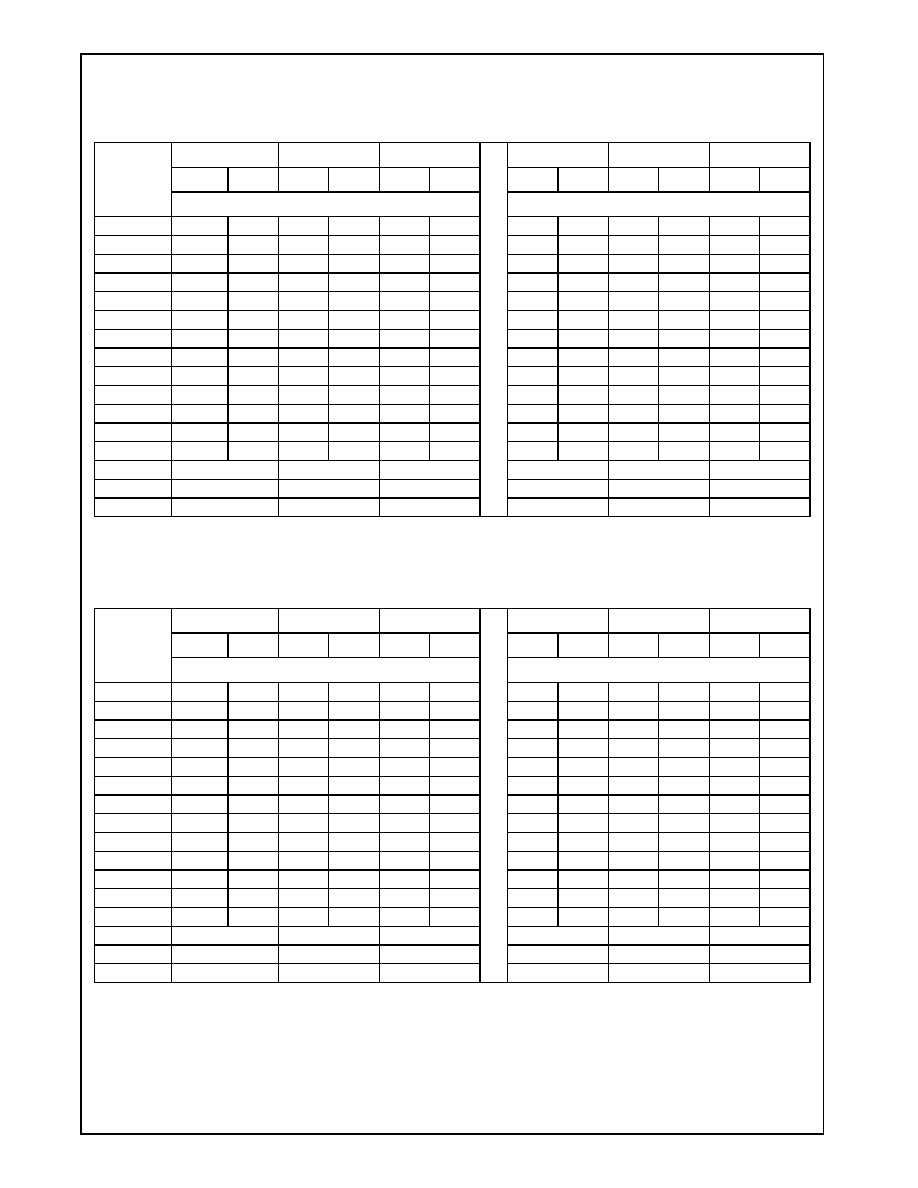
Revision 3.1
113
www.national.com
Integrated Functions (
Continued
)
GeodeTM
G
Xm
P
r
ocessor
Table 4-17. Auto LOI -- 2 DIMMs, Same Size, 1 DIMM Bank
1 K Page Size
2 K Page Size
4 K Page Size
1 K Page Size
2 K Page Size
4 Page Size
Row
Col
Row
Col
Row
Col
Row
Col
Row
Col
Row
Col
Address
2 Component Banks
4 Component Banks
MA12
A24
--
A25
--
A26
A25
--
A26
--
A27
MA11
A23
--
A24
--
A25
A24
--
A25
--
A26
MA10
A22
--
A23
--
A24
A23
--
A24
--
A25
MA9
A21
--
A22
--
A23
A22
A9
A23
--
A24
MA8
A20
--
A21
--
A22
A11
A21
A8
A22
--
A23
A11
MA7
A19
--
A20
A10
A21
A10
A20
A7
A21
A10
A22
A10
MA6
A18
A9
A19
A9
A20
A9
A19
A6
A20
A9
A21
A9
MA5
A17
A8
A18
A8
A19
A8
A18
A5
A19
A8
A20
A8
MA4
A16
A7
A17
A7
A18
A7
A17
A4
A18
A7
A19
A7
MA3
A15
A6
A16
A6
A17
A6
A16
A3
A17
A6
A18
A6
MA2
A14
A5
A15
A5
A16
A5
A15
A8
A16
A5
A17
A5
MA1
A13
A4
A14
A4
A15
A4
A14
A7
A15
A4
A16
A4
MA0
A12
A3
A13
A3
A14
A3
A13
A6
A14
A3
A15
A3
CS0#/CS1#
A11
A12
A13
A12
A13
A14
CS2#/CS#3
--
--
--
--
--
--
BA0/BA1
A10
A11
A12
A11/A10
A12/A11
A13/A12
Table 4-18. Auto LOI -- 2 DIMMs, Same Size, 2 DIMM Banks
1 K Page Size
2 K Page Size
4 K Page Size
1 K Page Size
2 Page Size
4 K Page Size
Row
Col
Row
Col
Row
Col
Row
Col
Row
Col
Row
Col
Address
2 Component Banks
4 Component Banks
MA12
A25
--
A26
--
A27
A26
--
A27
--
A28
--
MA11
A24
--
A25
--
A26
A25
--
A26
--
A27
--
MA10
A23
--
A24
--
A25
A24
--
A25
--
A26
--
MA9
A22
--
A23
--
A24
A23
--
A24
--
A25
--
MA8
A21
--
A22
--
A23
A11
A22
--
A23
--
A24
A11
MA7
A20
--
A21
A10
A22
A10
A21
--
A22
A10
A23
A10
MA6
A19
A9
A20
A9
A21
A9
A20
A9
A21
A9
A22
A9
MA5
A18
A8
A19
A8
A20
A8
A19
A8
A20
A8
A21
A8
MA4
A17
A7
A18
A7
A19
A7
A18
A7
A19
A7
A20
A7
MA3
A16
A6
A17
A6
A18
A6
A17
A6
A18
A6
A19
A6
MA2
A15
A5
A16
A5
A17
A5
A16
A5
A17
A5
A18
A5
MA1
A14
A4
A15
A4
A16
A4
A15
A4
A16
A4
A17
A4
MA0
A13
A3
A14
A3
A15
A3
A14
A3
A15
A3
A16
A3
CS0#/CS1#
A12
A13
A14
A13
A14
A15
CS2#/CS3#
A11
A12
A13
A12
A13
A14
BA0/BA1
A10
A11
A12
A11/A10
A12/A11
A13/A12
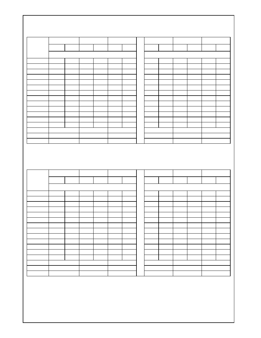
www.national.com
114
Revision 3.1
Integrated Functions (
Continued
)
GeodeTM
G
Xm
Pr
ocessor
Table 4-19. Non-Auto LOI -- 1 or 2 DIMMs, Different Sizes, 1 DIMM Bank
1 K Page Size
2 K Page Size
4 K Page Size
1 K Page Size
2 K Page Size
4 K Page Size
Row
Col
Row
Col
Row
Col
Row
Col
Row
Col
Row
Col
Address
2 Component Banks
4 Component Banks
MA12
A23
--
A24
--
A25
--
A24
--
A25
--
A26
MA11
A22
--
A23
--
A24
--
A23
--
A24
--
A25
MA10
A21
--
A22
--
A23
--
A22
--
A23
--
A24
MA9
A20
--
A21
--
A22
--
A21
--
A22
--
A23
MA8
A19
--
A20
--
A21
A11
A20
--
A21
--
A22
A11
MA7
A18
--
A19
A10
A20
A10
A19
--
A20
A10
A21
A10
MA6
A17
A9
A18
A9
A19
A9
A18
A9
A19
A9
A20
A9
MA5
A16
A8
A17
A8
A18
A8
A17
A8
A18
A8
A19
A8
MA4
A15
A7
A16
A7
A17
A7
A16
A7
A17
A7
A18
A7
MA3
A14
A6
A15
A6
A16
A6
A15
A6
A16
A6
A17
A6
MA2
A13
A5
A14
A5
A15
A5
A14
A5
A15
A5
A16
A5
MA1
A12
A4
A13
A4
A14
A4
A13
A4
A14
A4
A15
A4
MA0
A11
A3
A12
A3
A13
A3
A12
A3
A13
A3
A14
A3
CS0#/CS1#
--
--
--
--
--
--
CS2#/CS3#
--
--
--
--
--
--
BA0/BA1
A10
A11
A12
A11/A10
A12/A11
A13/A12
Table 4-20. Non-Auto LOI -- 1 or 2 DIMMs, Different Sizes, 2 DIMM Banks
1 K Page Size
2 K Page Size
4 K Page Size
1 K Page Size
2 K Page Size
4 K Page Size
Row
Col
Row
Col
Row
Col
Row
Col
Row
Col
Row
Col
Address
2 Component Banks
4 Component Banks
MA12
A24
--
A25
--
A26
--
A25
--
A26
--
A27
--
MA11
A23
--
A24
--
A25
--
A24
--
A25
--
A26
--
MA10
A22
--
A23
--
A24
--
A23
--
A24
--
A25
--
MA9
A21
--
A22
--
A23
--
A22
--
A23
--
A24
--
MA8
A20
--
A21
--
A22
A11
A21
--
A22
--
A23
A11
MA7
A19
--
A20
A10
A21
A10
A20
--
A21
A10
A22
A10
MA6
A18
A9
A19
A9
A20
A9
A19
A9
A20
A9
A21
A9
MA5
A17
A8
A18
A8
A19
A8
A18
A8
A19
A8
A20
A8
MA4
A16
A7
A17
A7
A18
A7
A17
A7
A18
A7
A19
A7
MA3
A15
A6
A16
A6
A17
A6
A16
A6
A17
A6
A18
A6
MA2
A14
A5
A15
A5
A16
A5
A15
A5
A16
A5
A17
A5
MA1
A13
A4
A14
A4
A15
A4
A14
A4
A15
A4
A16
A4
MA0
A12
A3
A13
A3
A14
A3
A13
A3
A14
A3
A15
A3
CS0#/CS1#
A11
A12
A13
A12
A13
A14
CS2#/CS3#
--
--
BA0/BA1
A10
A11
A12
A11/A10
A12/A11
A13/A12

Revision 3.1
115
www.national.com
Integrated Functions (
Continued
)
GeodeTM
G
Xm
P
r
ocessor
4.3.6
Memory Cycles
Figures 4-5 through Figure 4-8 on page 117 illustrate vari-
ous memory cycles that the memory controller supports.
The following subsections describe some of the sup-
ported cycles.
SDRAM Read Cycle
Figure 4-5 shows a SDRAM read cycle. The figure
assumes that a previous ACT command has presented
the row address for the read operation. Note that the burst
length for the READ command is always two.
Figure 4-5. Basic Read Cycle with a CAS Latency of Two
SDCLK
CS#
RAS#
CAS#
WE#
DQM
MD
MA
COL n
n
n+1
www.national.com
116
Revision 3.1
Integrated Functions (
Continued
)
GeodeTM
G
Xm
Pr
ocessor
SDRAM Write Cycle
Figure 4-6 shows a SDRAM write cycle. The burst length for the WRT command is 2.
Figure 4-6. Basic Write Cycle
SDCLK
CS#
RAS#
CAS#
WE#
MA
COL n
n
n+1
MD
n
n+1
DQM
Revision 3.1
117
www.national.com
Integrated Functions (
Continued
)
GeodeTM
G
Xm
P
r
ocessor
SDRAM Refresh Cycle
Figure 4-7 shows a SDRAM auto refresh cycle. The mem-
ory controller always precedes the refresh cycle with a
PRE command to all banks.
Page Miss
Figure 4-8 shows a Read/WRT command after a page
miss cycle. In order to program the new row address, a
PRE command must be issued followed by an ACT com-
mand.
Figure 4-7. Auto Refresh Cycle
Figure 4-8. Read/WRT Command to a New Row Address
SDCLK
CS#
RAS#
CAS#
WE#
MA[10]
SDCLK
COMMAND
ADDRESS
tRP
tRCD
PRE
NOP
NOP
ACT
NOP
NOP
R/W
NOP
ROW
COL
BA
www.national.com
118
Revision 3.1
Integrated Functions (
Continued
)
GeodeTM
G
Xm
Pr
ocessor
4.3.7
SDRAM Interface Clocking
The GXm processor drives the SDCLK to the SDRAMs;
one for each DIMM bank. All the control, data, and
address signals driven by the memory controller are sam-
pled by the SDRAM at the rising edge of SDCLK. SDCLK-
OUT is a reference signal used to generate SDCLKIN.
Read data is sampled by the memory controller at the ris-
ing edge of SDCLKIN.
The delay for SDCLKIN must be designed so that it lags
the SDCLKs at the DRAM by approximately 2ns. The
delay should also include the SDCLK transmission line
delay. The SDCLK traces on the board need to be laid out
so there is no skew between each of the four sinks. These
guidelines allow the memory interface to be closer to the
DRAM specifications. They improve performance by run-
ning the SDCLK up to frequencies of 100 MHz and a CAS
latency of two.
Figure 4-9. SDCLKIN Clocking
DIMM
0
DIMM
1
SDCLK[3:0]
Delay
SDCLKOUT
SDCLKIN
SDCLK0
SDCLK1
SDCLK2
SDCLK3
GeodeTM GXm
Processor

Revision 3.1
119
www.national.com
Integrated Functions (
Continued
)
GeodeTM
G
Xm
P
r
ocessor
The SDRAM interface timings are programmable. The
SHFTSDCLK bits in the MC_MEM_CNTRL2 register can
be used to change the relationship between SDCLK and
the control/address/data signals. To meet setup and hold
time requirements for SDRAM across different board lay-
outs, the SHFTSDCLK bits are used. SHFTSDCLK bit val-
ues are selected based upon the SDRAM signals loads
and the core frequency (refer to Table 7-10 on page 190 ).
Figure 4-10 shows an example of how the SHFTSDCLK
bits setting affects SDCLK. The PCI clock is the input
clock to the GXm processor. The core clock is the internal
processor clock that is multiplied up. The memory control-
ler runs off this processor clock. The memory clock is gen-
erated by dividing down the processor clock. SDCLK is
generated from the memory clock. In the example dia-
gram, the processor clock is running 6X times the PCI
clock and the memory clock is running in divide by 3
mode.
The SDRAM control, address, and data signals are driven
off edge "x" of the memory clock to be setup before edge
"y". With no shift applied, the control signals could end up
being latched on edge "x". A shift value of two or three
could be used so that SDCLK at the SDRAM is centered
around when the control signals change.
Figure 4-10. Effects of SHFTSDCLK Programming Bits Example
0
1
2
3
4
5
6
PCI Clock
Core Clock
Memory
Clock
(Internal)
(Internal)
CNTRL
SDCLK
SDCLK
(Note)
(Note)
Note: The first SDCLK shows how SDCLK operates with the SHFTSDCLK bits = 000, no shift.
The second SDCLK shows how SDCLK operates with the SHFTSDCLK bits = 001, shift 0.5 core clock.
(See MC_MEMCNTRL2 bits [5:3], Table 4-16 on page 108 , for remaining decode values.)
1
0
2
3
4
Shift =
Valid
x
y
x
y
www.national.com
120
Revision 3.1
Integrated Functions (
Continued
)
GeodeTM
G
Xm
Pr
ocessor
4.4
GRAPHICS PIPELINE
The graphics pipeline of the GXm processor includes a
BitBLT/vector engine which has been optimized for
Microsoft Windows. The hardware supports pattern gen-
eration, source expansion, pattern/source transparency,
and 256 ternary raster operations. The block diagram of
the graphics pipeline is shown in Figure 4-11.
4.4.1
BitBLT/Vector Engine
BLTs are initiated by writing to the GP_BLT_MODE regis-
ter, which specifies the type of source data (none, frame
buffer, or BLT buffer), the type of the destination data
(none, frame buffer, or BLT buffer), and a source expan-
sion flag.
Figure 4-11. Graphics Pipeline Block Diagram
Pattern
Hardware
Raster Operation
Output Aligner
BE
PAT
SRC
DST
BE
Internal Bus
Interface Unit
Graphics
Scratchpad RAM
BitBLT Buffers
and
Memory
X-Bus
C-Bus
Pipeline
BE = Byte Enable
PAT = Pattern Data
SRC = Source Data
DST = Destination Data
Output Aligner
Source
Expansion
Control Logic
DRAM Interface
Register Access
Controller
Key:
Revision 3.1
121
www.national.com
Integrated Functions (
Continued
)
GeodeTM
G
Xm
P
r
ocessor
The BLT buffers in the dedicated cache temporarily store
source and destination data, typically on a scan line basis.
The hardware automatically loads frame-buffer data
(source or destination) into the BLT buffers for each scan
line. The software is responsible for making sure that this
does not overflow the memory allocated for the BLT buff-
ers. When the source data is a bitmap, the data is loaded
directly into the BLT buffer before starting the BLT.
Vectors
are
initiated
by
writing
to
the
GP_VECTOR_MODE register (GX_BASE+8204h), which
specifies the direction of the vector and a "read destina-
tion data" flag. If the flag is set, the hardware will read
destination data along the vector and store it temporarily
in BLT Buffer 0.
4.4.2
Master/Slave Registers
When starting a BitBLT or vector operation, the graphics
pipeline registers are latched from the master registers to
the slave registers. A second BitBLT or vector operation
can then be loaded into the master registers while the first
operation is rendered. If a second BLT is pending in the
master registers, any write operations to the graphics
pipeline registers will corrupt the values of the pending
BLT. Software must prevent this from happening by check-
ing the "BLT Pending" bit in the GP_BLT_STATUS register
(GX_BASE+820Ch[2].
Most of the graphics pipeline registers are latched directly
from the master registers to the slave registers when
starting a new BitBLT or vector operation. Some registers,
however, use the updated slave values if the master regis-
ters have not been written, which allows software to ren-
der successive primitives without loading some of the
registers as outlined in Table 4-21.
4.4.3
Pattern Generation
The graphics pipeline contains hardware support for 8x8
monochrome patterns (expanded to two colors), 8x8
dither patterns (expanded to four colors), and 8x1 color
patterns. The pattern hardware, however, does not main-
tain a pattern origin, so the pattern data must be justified
before it is loaded into the GXm processor's registers. For
solid primitives, the pattern hardware is disabled and the
pattern
color
is
always
sourced
from
the
GP_PAT_COLOR_0 register (GX_BASE+8110h).
Table 4-21. Graphics Pipeline Registers
Master
Function
GP_DST_XCOOR
Next X position along vector.
Master register if written, otherwise:
Unchanged slave if BLT, source mode = bitmap.
Slave + width if BLT, source mode = text glyph
GP_DST_YCOOR
Next Y position along vector.
Master register if written, otherwise:
Slave +/- height if BLT, source mode = bitmap.
Unchanged slave if BLT, source mode = text glyph.
GP_INIT_ERROR
Master register if written, otherwise:
Initial error for the next pixel along the vector.
GP_SRC_YCOOR
Master register if written, otherwise:
Slave +/- height if BLT, source mode = bitmap.

www.national.com
122
Revision 3.1
Integrated Functions (
Continued
)
GeodeTM
G
Xm
Pr
ocessor
4.4.3.1
Monochrome Patterns
Monochrome patterns are selected by setting the pattern
mode to 01b in the GP_RASTER_MODE register
(GX_BASE+ 8200h). Those pixels corresponding to a
clear bit (0) in the pattern are rendered using the color
specified in the GP_PAT_COLOR_0 register, and those
pixels corresponding to a set bit (1) in the pattern are ren-
dered using the color specified in the GP_PAT_COLOR_1
register (GX_BASE+8112h).
If the pattern transparency bit is set high in the
GP_RASTER_MODE register, those pixels corresponding
to a clear bit in the pattern data are not drawn.
Monochrome patterns use bits [63:0] of the pattern data.
Bits [7:0] correspond to the first row of the pattern, and bit
7 corresponds to the leftmost pixel on the screen. This is
illustrated in Figure 4-12.
Figure 4-12. Example of Monochrome Patterns
4.4.3.2
Dither Patterns
Dither patterns are selected by setting the pattern mode
to 10 b in the GP_RASTER_MODE register (Table 4-25
on page 125). Two bits of pattern data are used for each
pixel, allowing color expansion to four colors. The colors
are
specified
in
the
GP_PAT_COLOR_0
through
GP_PAT_COLOR_3 registers (Table 4-25 on page 125).
Dither patterns use all 128 bits of pattern data. Bits [15:0]
correspond to the first row of the pattern (the lower byte
contains the LSB of the pattern color and the upper byte
contains the MSB of the pattern color). This is illustrated
in Figure 4-13.
Figure 4-13. Example of Dither Patterns
GP_PAT_DATA_0 = 0x80412214
GP_PAT_DATA_1 = 0x08142241
14
22
41
80
41
22
14
08
00AA
4411
00AA
1155
00AA
4411
00AA
1155
GP_PAT_DATA_0 = 0x441100AA
GP_PAT_DATA_1 = 0x115500AA
GP_PAT_DATA_2 = 0x441100AA
GP_PAT_DATA_3 = 0x115500AA
Revision 3.1
123
www.national.com
Integrated Functions (
Continued
)
GeodeTM
G
Xm
P
r
ocessor
4.4.3.3
Color Patterns
Color patterns are selected by setting the pattern mode to
11 b in the GP_RASTER_MODE register. Bits [63:0] are
used to hold a row of pattern data for an 8-BPP pattern,
with bits [7:0] corresponding to the leftmost pixel of the
row. Likewise, bits [127:0] are used for a 16-BPP color
pattern, with bits [15:0] corresponding to the leftmost pixel
of the row.
To support an 8x8 color pattern, software must load the
pattern data for each row.
4.4.4
Source Expansion
The graphics pipeline contains hardware support for color
expansion of source data (primarily used for text). Those
pixels corresponding to a clear bit (0) in the source data
are
rendered
using
the
color
specified
in
the
GP_SRC_COLOR_0 register (GX_BASE+810Ch), and
those pixels corresponding to a set bit (1) in the source
data are rendered using the color specified in the
GP_SRC_COLOR_1 register (GX_BASE+810Eh).
If
the
source
transparency
bit
is
set
in
the
GP_RASTER_MODE register, those pixels corresponding
to a clear bit (0) in the source data are not drawn.
4.4.5
Raster Operations
The GP_RASTER_MODE register specifies how the pat-
tern data, source data (color-expanded if necessary), and
destination data are combined to produce the output from
the graphics pipeline. The definition of the ROP valu
matches that of the Microsoft API. This allows Windows
display drivers to load the raster operation directly into
hardware. Table 4-22 illustrates this definition. Some com-
mon raster operations are described in Table 4-23.
Table 4-22. GP_RASTER_MODE Bit Patterns
Pattern
(bit)
Source
(bit)
Destination
(bit)
Output
(bit)
0
0
0
ROP[0]
0
0
1
ROP[1]
0
1
0
ROP[2]
0
1
1
ROP[3]
1
0
0
ROP[4]
1
0
1
ROP[5]
1
1
0
ROP[6]
1
1
1
ROP[7]
Table 4-23. Common Raster Operations
ROP
Description
F0h
Output = Pattern
CCh
Output = source
5Ah
Output = Pattern XOR destination
66h
Output = Source XOR destination
55h
Output = ~Destination

www.national.com
124
Revision 3.1
Integrated Functions (
Continued
)
GeodeTM
G
Xm
Pr
ocessor
4.4.6
Graphics Pipeline Register Descriptions
The graphics pipeline maps 200h locations starting at
GX_BASE+8100h. Refer to Section 4.1.2 "Control Regis-
ters" on page 94 for instructions on accessing these regis-
ters.
Table 4-24 summarizes the graphics pipeline registers
and Table 4-25 on page 125 gives detailed register/bit for-
mats.
Table 4-24. Graphics Pipeline Configuration Register Summary
GX_BASE+
Memory Offset
Type
Name / Function
Default Value
8100h-8103h
R/W
GP_DST/START_Y/XCOOR
Destination/Starting Y and X Coordinates Register -- In BLT mode this register
specifies the destination Y and X positions for a BLT operation. In Vector mode it
specifies the starting Y and X positions in a vector.
00000000h
8104-8107h
R/W
GP_WIDTH/HEIGHT and GP_VECTOR_LENGTH/INIT_ERROR
Width/Height or Vector Length/Initial Error Register -- In BLT mode this register
specifies the BLT width and height in pixels. In Vector mode it specifies the vector
initial error and pixel length.
00000000h
8108h-810Bh
R/W
GP_SRC_X/YCOOR and GP_AXIAL/DIAG_ERROR
Source X/Y Coordinate Axial/Diagonal Error Register -- In BLT mode this register
specifies the BLT X and Y source. In Vector mode it specifies the axial and diago-
nal error for rendering a vector.
00000000h
810Ch-810Fh
R/W
GP_SRC_COLOR_0 and GP_SCR_COLOR_1
Source Color Register -- Determines the colors used when expanding mono-
chrome source data in either the 8-BPP mode or the 16-BPP mode.
00000000h
8110h-8113h
R/W
GP_PAT_COLOR_0 and GP_PAT_COLOR_1
Graphics Pipeline Pattern Color 0 and 1 Registers -- These two registers deter-
mine the colors used when expanding pattern data.
00000000h
8114h-8117h
R/W
GP_PAT_COLOR_2 and GP_PAT_COLOR_3
Graphics Pipeline Pattern Color 2 and 3 Registers -- These two registers deter-
mine the colors used when expanding pattern data.
00000000h
8120h-8123h
R/W
GP_PAT_DATA 0 through 3
Graphics Pipeline Pattern Data Registers 0 through 3 -- Together these registers
contain 128 bits of pattern data.
GP_PAT_DATA_0 corresponds to bits [31:0] of the pattern data.
GP_PAT_DATA_1 corresponds to bits [63:32] of the pattern data.
GP_PAT_DATA_2 corresponds to bits [95:64] of the pattern data.
GP_PAT_DATA_3 corresponds to bits [127:96] of the pattern data.
00000000h
8124h-8127h
R/W
00000000h
8128h-812Bh
R/W
00000000h
812Ch-812Fh
R/W
00000000h
8140h-8143h
(Note)
R/W
GP_VGA_WRITE
Graphics Pipeline VGA Write Patch Control Register -- Controls the VGA mem-
ory write path in the graphics pipeline.
xxxxxxxxh
8144h-8147h
(Note)
R/W
GP_VGA_READ
Graphics Pipeline VGA Read Patch Control Register -- Controls the VGA mem-
ory read path in the graphics pipeline.
00000000h
8200h-8203h
R/W
GP_RASTER_MODE
Graphics Pipeline Raster Mode Register -- This register controls the manipula-
tion of the pixel data through the graphics pipeline. Refer to Section 4.4.5 "Raster
Operations" on page 123.
00000000h
8204h-8207h
R/W
GP_VECTOR_MODE
Graphics Pipeline Vector Mode Register -- Writing to this register initiates the
rendering of a vector.
00000000h
8208h-820Bh
R/W
GP_BLT_MODE
Graphics Pipeline BLT Mode Register -- Writing to this initiates a BLT operation.
00000000h
Note: The registers at GX_BASE+8140, 8144h, 8210h, and 8217h are located in the area designated for the graphics pipeline but
are used for VGA emulation purposes. Refer to Table 5-5 on page 173 for these register's bit formats.
Revision 3.1
125
www.national.com
Integrated Functions (
Continued
)
GeodeTM
G
Xm
P
r
ocessor
820Ch-820Fh
R/W
GP_BLT_STATUS
Graphics Pipeline BLT Status Register -- Contains configuration and status infor-
mation for the BLT engine. The status bits are contained in the lower byte of the
register.
00000000h
8210h-8213h
(Note)
R/W
GP_VGA_BASE
Graphics Pipeline VGA Memory Base Address Register -- Specifies the offset of
the VGA memory, starting from the base of graphics memory.
xxxxxxxxh
8214h-8217h
(Note)
R/W
GP_VGA_LATCH
Graphics Pipeline VGA Display Latch Register -- Provides a memory mapped
way to read or write the VGA display latch.
xxxxxxxxh
Table 4-24. Graphics Pipeline Configuration Register Summary (Continued)
GX_BASE+
Memory Offset
Type
Name / Function
Default Value
Note: The registers at GX_BASE+8140, 8144h, 8210h, and 8217h are located in the area designated for the graphics pipeline but
are used for VGA emulation purposes. Refer to Table 5-5 on page 173 for these register's bit formats.
Table 4-25. Graphics Pipeline Configuration Registers
Bit
Name
Description
GX_BASE+8100h-8103h
GP_DST/START_X/YCOOR Register (R/W)
Default Value = 00000000h
31:16
DESTINATION/STARTING Y POSITION (SIGNED):
BLT Mode -- Specifies the destination Y position for a BLT operation.
Vector Mode -- Specifies the starting Y position in a vector.
15:0
DESTINATION/STARTING X POSITION (SIGNED):
BLT Mode -- Specifies the destination X position for a BLT operation.
Vector Mode -- Specifies the starting X position in a vector.
GX_BASE+8104h-8107h
GP_WIDTH/HEIGHT and
Default Value = 00000000h
GP_VECTOR_LENGTH/INIT_ERROR Register (R/W)
31:16
PIXEL_WIDTH or VECTOR_LENGTH (UNSIGNED):
BLT Mode -- Specifies the width, in pixels, of a BLT operation. No pixels are rendered for a width of zero.
Vector Mode -- Bits [31:30] are reserved in this mode allowing this 14-bit field to specify the length, in pixels, of a vector. No
pixels are rendered for a length of zero. This field is limited to 14 bits due to a lack of precision in the registers used to hold
the error terms.
15:0
PIXEL_HEIGHT or VECTOR_INITIAL_ERROR (UNSIGNED):
BLT Mode -- Specifies the height, in pixels, of a BLT operation. No pixels are rendered for a height of zero.
Vector Mode -- Specifies the initial error for renderng a vector.
GX_BASE+8108h-810Bh
GP_SCR_X/YCOOR and GP_AXIAL/DIAG_ERROR Register (R/W)
Default Value = 00000000h
31:16
SRC_X_POS or VECTOR_AXIAL_ERROR (SIGNED):
BLT Mode -- Specifies the source X position for a BLT operation.
Vector Mode -- Specifies the axial error for rendering a vector.
15:0
SRC_Y_POS or VECTOR_DIAG_ERROR (SIGNED):
Source Y Position (Signed) -- Specifies the source Y position for a BLT operation.
Vector Mode -- Specifies the diagonal error for rendering a vector.
GX_BASE+810Ch-810Fh
GP_SRC_COLOR Register (R/W)
Default Value = 00000000h
8-BPP Mode
31:24
GP_SRC_COLOR_0:
8-BPP Color Index -- The color index must be duplicated in the upper byte of GP_SRC_COLOR_0 when rendering 8-BPP
data.
23:16
15:8
GP_SRC_COLOR_1:
8-BPP Color Index -- The color index must be duplicated in the upper byte of GP_SRC_COLOR_1 when rendering 8-BPP
data.
7:0
16-BPP Mode
31:16
GP_SRC_COLOR_0: 16-BPP Color (RGB)
15:0
GP_SRC_COLOR_1: 16-BPP Color (RGB)

www.national.com
126
Revision 3.1
Integrated Functions (
Continued
)
GeodeTM
G
Xm
Pr
ocessor
Note: The Graphics Pipeline Source Color Register specifies the colors used when expanding monochrome source data in either the
8-BPP mode or the 16-BPP mode. Those pixels corresponding to clear bits (0) in the source data are rendered using
GP_SRC_COLOR_0 and those pixels corresponding to set bits (1) in the source data are rendered using
GP_SRC_COLOR_1.
GX_BASE+8110h-8113h
GP_PAT_COLOR_A Register (R/W)
Default Value = 00000000h
8-BPP Mode
31:24
GP_PAT_COLOR_0:
8-BPP Color Index -- The color index must be duplicated in the upper byte of GP_PAT_COLOR_0 when rendering 8-BPP
data.
23:16
15:8
GP_PAT_COLOR_1:
8-BPP Color Index -- The color index must be duplicated in the upper byte of GP_PAT_COLOR_1 when rendering 8-BPP
data.
7:0
16-BPP Mode
31:16
GP_PAT_COLOR_0: 16-BPP Color (RGB)
15:0
GP_PAT_COLOR_1: 16-BPP Color (RGB)
Note: The Graphics Pipeline Pattern Color A and B Registers specify the colors used when expanding pattern data.
GX_BASE+8114h-8117h
GP_PAT_COLOR_B Register (R/W)
Default Value = 00000000h
8-BPP Mode
31:24
GP_PAT_COLOR_2:
8-BPP Color Index -- The color index must be duplicated in the upper byte of GP_PAT_COLOR_2 when rendering 8-BPP
data.
23:16
15:8
GP_PAT_COLOR_3:
8-BPP Color Index -- The color index must be duplicated in the upper byte of GP_PAT_COLOR_3 when rendering 8-BPP
data.
7:0
16-BPP Mode
31:16
GP_PAT_COLOR_2: 16-BPP Color (RGB)
15:0
GP_PAT_COLOR_3: 16-BPP Color (RGB)
Note: The Graphics Pipeline Pattern Color A and B Registers specify the colors used when expanding pattern data.
GX_BASE+8120h-8123h
GP_PAT_DATA_0 Register (R/W)
Default Value = 00000000h
31:0
GP Pattern Data Register 0: The Graphics Pipeline Pattern Data Registers 0 through 3 together contain 128 bits of pat-
tern data. The GP_PAT_DATA_0 register corresponds to bits [31:0] of the pattern data.
GX_BASE+8124h-8127h
GP_PAT_DATA_1 Register (R/W)
Default Value = 00000000h
31:0
GP Pattern Data Register 1: The Graphics Pipeline Pattern Data Registers 0 through 3 together contain 128 bits of pat-
tern data. The GP_PAT_DATA_1 register corresponds to bits [63:32] of the pattern data.
GX_BASE+8128h-812Bh
GP_PAT_DATA_2 Register (R/W)
Default Value = 00000000h
31:0
GP Pattern Data Register 2: The Graphics Pipeline Pattern Data Registers 0 through 3 together contain 128 bits of pat-
tern data. The GP_PAT_DATA_2 register corresponds to bits [95:64] of the pattern data.
GX_BASE+812Ch-812Fh
GP_PAT_DATA_3 Register (R/W)
Default Value = 00000000h
31:0
GP Pattern Data Register 3: The Graphics Pipeline Pattern Data Registers 0 through 3 together contain 128 bits of pat-
tern data. The GP_PAT_DATA_3 register corresponds to bits [127:96] of the pattern data.
GX_BASE+8140h-8143h
GP_VGA_WRITE Register (R/W)
Default Value = xxxxxxxxh
Note that the registers at GX_BASE+82140h and 8144h are located in the area designated for the graphics pipeline but are used for
VGA emulation purposes. Refer to Table 5-5 on page 173 for these register's bit formats.
GX_BASE+8144h-8147h
GP_VGA_READ Register (R/W)
Default Value = 00000000h
Note that the registers at GX_BASE+82140h and 8144h are located in the area designated for the graphics pipeline but are used for
VGA emulation purposes. Refer to Table 5-5 on page 173 for these register's bit formats.
Table 4-25. Graphics Pipeline Configuration Registers (Continued)
Bit
Name
Description
Revision 3.1
127
www.national.com
Integrated Functions (
Continued
)
GeodeTM
G
Xm
P
r
ocessor
GX_BASE+8200h-8203h
GP_RASTER_MODE Register (R/W)
Default Value = 00000000h
31:13
RSVD
Reserved: Set to 0.
12
TB
Transparent BLIT: When set, this bit enables transparent BLIT. The source color data will be compared to a
color key and if it matches, that pixel will not be drawn. The color key value is stored in the BLIT buffer as
destination data. The raster operation must be set to C6h, and the pattern registers must be all F's for this
mode to work properly.
11
ST
Source Transparency: Enables transparency for monochrome source data. Those pixels corresponding to
clear bits in the source data are not drawn.
10
PT
Pattern Transparency: Enables transparency for monochrome pattern data. Those pixels corresponding to
clear bits in the pattern data are not drawn.
9:8
PM
Pattern Mode: Specifies the format of the pattern data.
00 = Indicates a solid pattern. The pattern data is always sourced from the GP_PAT_COLOR_0 register.
01 = Indicates a monochrome pattern. The pattern data is sourced from the GP_PAT_COLOR_0 and
GP_PAT_COLOR_1 registers.
10 = Indicates a dither pattern. All four pattern color registers are used.
11 =Indicates a color pattern. The pattern data is sourced directly from the pattern data registers.
7:0
ROP
Raster Operation: Specifies the raster operation for pattern, source, and destination data.
GX_BASE+8204h-8207h
GP_VECTOR_MODE Register (R/W)
Default Value = 00000000h
31:4
RSVD
Reserved: Set to 0.
3
DEST
Read Destination Data: Indicates that frame-buffer destination data is required.
2
DMIN
Minor Direction: Indicates a positive minor axis step.
1
DMAJ
Major Direction: Indicates a positive major axis step.
0
YMAJ
Major Direction: Indicates a Y Major vector.
GX_BASE+8208h-820Bh
GP_BLT_MODE Register (R/W)
Default Value = 00000000h
31:9
RSVD
Reserved: Set to 0.
8
Y
Reverse Y Direction: Indicates a negative increment for the Y position. This bit is used to control the direc-
tion of screen to screen BLTs to prevent data corruption in overlapping windows.
7:6
SM
Source Mode: Specifies the format of the source data.
00 = Source is a color bitmap.
01 = Source is a monochrome bitmap (use source color expansion).
10 = Unused.
11 = Source is a text glyph (use source color expansion). This differs from a monochrome bitmap in that the
X position is adjusted by the width of the BLT and the Y position remains the same.
5
RSVD
Reserved: Set to 0.
4:2
RD
Destination Data: Specifies the destination data location.
000 = No destination data is required. The destination data into the raster operation unit is all ones.
010 = Read destination data from BLT Buffer 0.
011 = Read destination data from BLT Buffer 1.
100 = Read destination data from the frame buffer (store temporarily in BLT Buffer 0).
101 = Read destination data from the frame buffer (store temporarily in BLT Buffer 1).
1:0
RS
Source Data: Specifies the source data location.
00 = No source data is required. The source data into the raster operation unit is all ones.
01 = Read source data from the frame buffer (temporarily stored in BLT Buffer 0).
10 = Read source data from BLT Buffer 0.
11 = Read source data from BLT Buffer 1.
Table 4-25. Graphics Pipeline Configuration Registers (Continued)
Bit
Name
Description
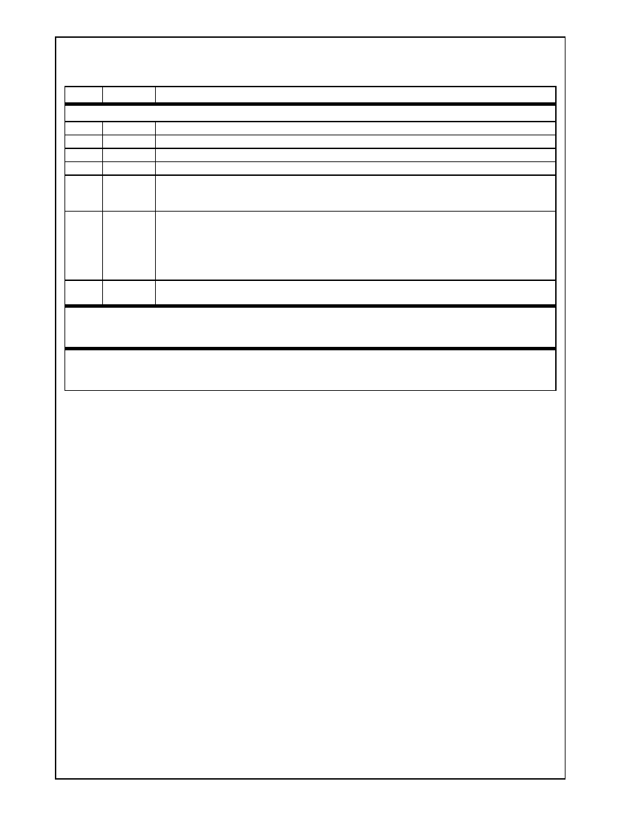
www.national.com
128
Revision 3.1
Integrated Functions (
Continued
)
GeodeTM
G
Xm
Pr
ocessor
GX_BASE+820Ch-820Fh
GP_BLT_STATUS Register (R/W)
Default Value = 00000000h
31:10
RSVD
Reserved: Set to 0.
9
W
Screen Width: Selects a frame-buffer width of 2048 bytes (default is 1024 bytes).
8
M
16-BPP Mode: Selects a pixel data format of 16 BPP (default is 8 BPP).
7:3
RSVD
Reserved: Set to 0.
2
BP (RO)
BLT Pending (Read Only): Indicates that a BLT operation is pending in the master registers.
The "BLT Pending" bit must be clear before loading any of the graphics pipeline registers. Loading registers
when this bit is set high will destroy the values for the pending BLT.
1
PB (RO)
Pipeline Busy (Read Only): Indicates that the graphics pipeline is processing data.
The "Pipeline Busy" bit differs from the "BLT Busy" bit in that the former only indicates that the graphics pipe-
line is processing data. The "BLT Busy" bit also indicates that the memory controller has not yet processed
all of the requests for the current operation.
The "Pipeline Busy" bit must be clear before loading a BLT buffer if the previous BLT operation used the
same BLT buffer.
0
BB (RO)
BLT Busy (Read Only): Indicates that a BLT / vector operation is in progress.
The "BLT Busy" bit must be clear before accessing the frame buffer directly.
GX_BASE+8210h-8213h
GP_VGA_BASE (R/W)
Default Value = xxxxxxxxh
Note that the registers at GX_BASE+8210h and 8214h are located in the area designated for the graphics pipeline but are used for
VGA emulation purposes. Refer to Table 5-5 on page 173 for these register's bit formats.
GX_BASE+8214h-8217h
GP_VGA_LATCH Register (R/W)
Default Value = xxxxxxxxh
Note that the registers at GX_BASE+8210h and 8214h are located in the area designated for the graphics pipeline but are used for
VGA emulation purposes. Refer to Table 5-5 on page 173 for these register's bit formats.
Table 4-25. Graphics Pipeline Configuration Registers (Continued)
Bit
Name
Description

Revision 3.1
129
www.national.com
Integrated Functions (
Continued
)
GeodeTM
G
Xm
P
r
ocessor
4.5
DISPLAY CONTROLLER
The GXm processor incorporates a display controller that
retrieves display data from the memory controller and for-
mats it for output on a variety of display devices. The GXm
processor can directly connect to an active matrix TFT
LCD flat panel or to an external RAMDAC for CRT display
or both. The display controller includes a display FIFO,
compression/decompression (CODEC) hardware, hard-
ware cursor, a 256-entry-by-18-bit palette RAM (plus
three extension colors), display timing generator, dither
and frame-rate-modulation circuitry for TFT panels, and
flexible output formatting logic. A diagram of the display
controller subsystem is shown in Figure 4-14.
Figure 4-14. Display Controller Block Diagram
Memory
Data
Compressed
Codec
Cursor
Palette
Extensions
Palette
Dither
Output
RAMDAC
Panel
Control Registers
Timing
Memory
Memory
Address
Output
Control
Pseudo/True
Color Mux
32
64
Line Buffer
(64x32 bit)
Display
FIFO
(64x64 bit)
Latch
8
2
32
RAM
(264x18
9
16
18
Palette Data
and
FRM
Format
8
18
18
Addr.
Logic
Generator
and
Control Logic
Address
Generator
20
9
18
bit)

www.national.com
130
Revision 3.1
Integrated Functions (
Continued
)
GeodeTM
G
Xm
Pr
ocessor
4.5.1
Display FIFO
The display controller contains a large (64x64 bit) FIFO for
queuing up display data from the memory controller as it
is required for output to the screen. The memory control-
ler must arbitrate between the display controller requests
and other requests for memory access from the micropro-
cessor core, L1 cache controller, and the graphics pipe-
line.
Since display data is required in real time, this data is the
highest priority in the system. Without efficient memory
management, system performance would suffer dramati-
cally due to the constant display-refresh requests from the
display controller. The large size of the display FIFO is
desirable so that the FIFO may primarily be loaded during
times when there is no other request pending to the
DRAM controller and so that the memory controller can
stay in page mode for a long period of time when servicing
the display FIFO. When a priority request from the cache
or graphics pipeline occurs, if the display FIFO has
enough data queued up, the DRAM controller can imme-
diately service the request without concern that the dis-
play FIFO will underflow. If the display FIFO is below a
programmable threshold, a high-priority request will be
sent to the DRAM controller, which will take precedence
over any other requests that are pending.
The display FIFO is 64 bits wide to accommodate high-
speed burst read operations from the DRAM controller at
maximum memory bandwidth. In addition to the normal
pixel data stream, the display FIFO also queues up cursor
patterns.
4.5.2
Compression Technology
To reduce the system memory contention caused by the
display refresh, the display controller contains compres-
sion and decompression logic for compressing the frame
buffer image in real time as it is sent to the display. It com-
bines this compressed display buffer into the extra off-
screen memory within the graphics memory aperture.
Coherency of the compressed display buffer is maintained
by use of dirty and valid bits for each line. The dirty and
valid RAM is contained on-chip for maximum efficiency.
Whenever a line has been validly compressed, it will be
retrieved from the compressed display buffer for all future
accesses until the line becomes dirty again. Dirty lines will
be retrieved from the normal uncompressed frame buffer.
The compression logic has the ability to insert a program-
mable number of "static" frames, during which time dirty
bits are ignored and the valid bits are read to determine
whether a line should be retrieved from the frame buffer or
compressed display buffer. The less frequently the dirty
bits are sampled, the more frequently lines will be
retrieved from the compressed display buffer. This allows
a programmable screen image update rate (as opposed to
refresh rate). Generally, an update rate of 30 frames per
second is adequate for displaying most types of data,
including real- time video. However, if a flat panel display
is used that has a slow response time, such as 100 ms,
the image need not be updated faster than ten frames per
second, since the panel could not display changes
beyond that rate.
The compression algorithm used in the GXm processor
commonly achieves compression ratios between 10:1 and
20:1, depending on the nature of the display data. This
high level of compression provides higher system perfor-
mance by reducing typical latency for normal system
memory access, higher graphics performance by increas-
ing available drawing bandwidth to the DRAM array, and
much lower power consumption by significantly reducing
the number of off-chip DRAM accesses required for
refreshing the display. These advantages become even
more pronounced as display resolution, color depth, and
refresh rate are increased and as the size of the installed
DRAM increases.
As uncompressed lines are fed to the display, they will be
compressed and stored in an on-chip compressed line
buffer (64x32 bits). Lines will not be written back to the
compressed display buffer in the DRAM unless a valid
compression has resulted, so there is no penalty for
pathological frame buffer images where the compression
algorithm breaks down.
4.5.3
Motion Video Acceleration Support
The display controller of the GXm processor supports the
CS5530 and future I/O companion chips' hardware motion
video acceleration by reading the off-screen video buffer
and serializing the video data onto the RAMDAC port. The
display controller supplies video data to the I/O compan-
ion chips in either interleaved YUV4:2:2 format or
RGB5:6:5 format. The I/O companion chips can then
scale and filter the data, apply color space conversion to
YUV data, and mix the video data with graphics data also
supplied by the display controller.

Revision 3.1
131
www.national.com
Integrated Functions (
Continued
)
GeodeTM
G
Xm
P
r
ocessor
4.5.4
Hardware Cursor
The display controller contains hardware cursor logic to
allow overlay of the cursor image onto the pixel data
stream. Overhead for updating this image on the screen is
kept to a minimum by requiring that only the X and Y posi-
tion be changed. This eliminates "submarining" effects
commonly associated with software cursors. The cursor,
32x32 pixels with two bits per pixel, is loaded into off-
screen memory within the graphics memory aperture. The
two-bit code selects color 0, color 1, transparent, or back-
ground-color inversion for each pixel in the cursor (see
Table 4-31 on page 144. The two cursor colors will be
stored as extensions to the normal 256-entry palette at
locations 100h and 101h. These palette extensions will be
used when driving a flat panel or a RAMDAC operating in
16 BPP (bits per pixel) mode. For 8 BPP operation using
an external RAMDAC, the DC_CURSOR_COLOR regis-
ter (GX_BASE+8360h) should be programmed to set the
indices for the cursor colors. To avoid corruption of the
cursor colors by an application program that modifies the
external palette, care should be taken to program the cur-
sor color indices to one of the static color indices. Since
Microsoft Windows typically uses only black and white
cursor colors and these are static colors, this kind of prob-
lem should rarely occur.
4.5.5
Display Timing Generator
The display controller features a fully programmable tim-
ing generator for generating all timing control signals for
the display. The timing control signals include horizontal
and vertical sync and blank signals in addition to timing for
active and overscan regions of the display. The timing
generator is similar in function to the CRTC of the original
VGA, although programming is more straightforward. Pro-
gramming of the timing registers will generally happen via
a BIOS INT10 call during a mode set. When programming
the timing registers directly, extreme care should be taken
to ensure that all timing is compatible with the display
device.
The timing generator supports overscan to maintain full
backward compatibility with the VGA. This feature is sup-
ported primarily for CRT display devices since flat panel
displays have fixed resolutions and do not provide for
overscan. However, the GXm processor supports a mech-
anism to center the display when a display mode is
selected having a lower resolution than the panel resolu-
tion. The border region is effectively stretched to fill the
remainder of the screen. The border color is at palette
extension 104h. For 8 BPP operation with an external
RAMDAC,
the
DC_BORDER_COLOR
register
(GX_BASE+8368h) should also be programmed.
4.5.6
Dither and Frame-Rate Modulation
The display controller supports 2x2 dither and two-level
frame-rate modulation (FRM) to increase the apparent
number of colors displayed on 9-bit or 12-bit TFT panels.
Dither and FRM are individually programmable. With dith-
ering and FRM enabled, 185,193 colors are possible on a
9-bit TFT panel, and 226,981 colors are possible on a 12-
bit TFT panel.
4.5.7
Display Modes
The GXm processor supports 640x480, 800x600, and
1024x768 display resolutions at both 8 and 16 bits per
pixel. In addition, 1280x1024 resolution is supported at 8
bits per pixel only. Two 16-bit display formats are sup-
ported: RGB 5-6-5 and RGB 5-5-5. All CRT modes use
VESA-compatible timing. Table 4-26 on page 132 gives
the supported CRT display modes.

www.national.com
132
Revision 3.1
Integrated Functions (
Continued
)
GeodeTM
G
Xm
Pr
ocessor
Table 4-26. TFT Panel Display Modes
Resolution
Simultaneous
Colors
Refresh
Rate
(Hz)
DOTCLK
Rate
(MHz)
PCLK
(MHz)
Panel
Type
Maximum Displayed
Colors (Note 1)
640x480
(Note 2)
8 BPP
256 colors out of a
palette of 256
60
25.175
25.175
9-bit
57
3
= 185,193
12-bit
61
3
= 226,981
18-bit
4
3
= 262,144
16 BPP
64 K colors
5-6-5
60
25.175
25.175
9-bit
29x57x29 = 47,937
12-bit
31x61x31 = 58,621
18-bit
32x64x32 = 65,535
800x600
(Note 2)
8 BPP
256 colors out of a
palette of 256
60
40.0
40.0
9-bit
57
3
= 185,193
12-bit
61
3
= 226,981
18-bit
64
3
= 262,144
16 BPP
64 K Colors
5-6-5
60
40.0
40.0
9-bit
29x57x29 = 47,937
12-bit
31x61x31 = 58,621
18-bit
32x64x32 = 65,535
1024x768
8 BPP
256 colors out of a
palette of 256
60
65
32.5
9-bit/18-I/F
57
3
= 185,193
16 BPP
64 K colors
5-6-5
60
65
32.5
9-bit/18-I/F
29x57x29 = 47,937
Notes: 1) 9-bit and 12-bit panels use FRM and dither to increase displayed colors. (See Section 4.5.6 "Dither and
Frame-Rate Modulation" on page 131.)
2) All 640x480 and 800x600 modes can be run in simultaneous display with CRT.

Revision 3.1
133
www.national.com
Integrated Functions (
Continued
)
GeodeTM
G
Xm
P
r
ocessor
Table 4-27. TFT Panel Data Bus Formats
Panel Data
Bus Bit
18-Bit
TFT
12-Bit
TFT
9-Bit TFT
640x480
1024x768
17
R5
R5
R5
R5
Even
16
R4
R4
R4
R4
15
R3
R3
R3
R3
14
R2
R2
R5
Odd
13
R1
R4
12
R0
R3
11
G5
G5
G5
G5
Even
10
G4
G4
G4
G4
9
G3
G3
G3
G3
8
G2
G2
G5
Odd
7
G1
G4
6
G0
G3
5
B5
B5
B5
B5
Even
4
B4
B4
B4
B4
3
B3
B3
B3
B3
2
B2
B2
B5
Odd
1
B1
B4
0
B0
B3
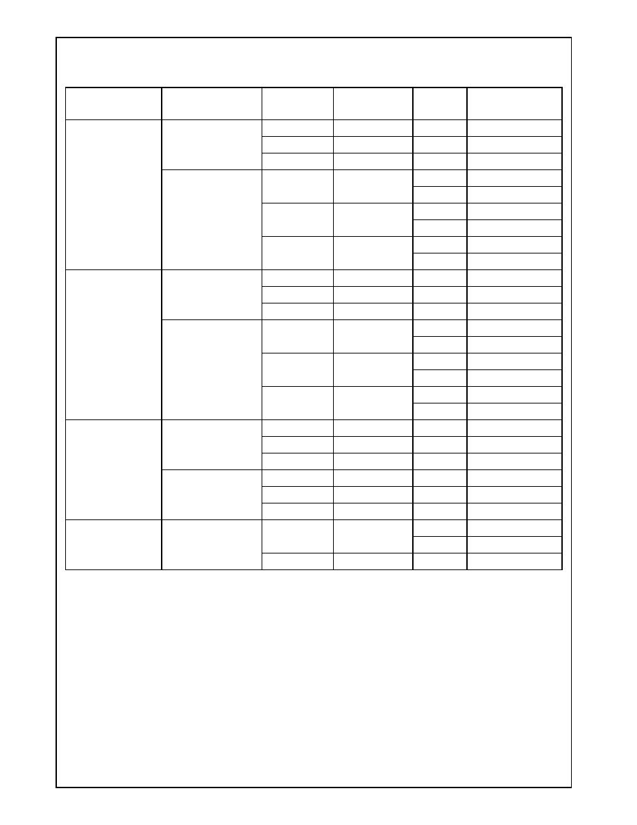
www.national.com
134
Revision 3.1
Integrated Functions (
Continued
)
GeodeTM
G
Xm
Pr
ocessor
Table 4-28. CRT Display Modes
Resolution
Simultaneous
Colors
Refresh Rate
(Hz)
DOTCLK Rate
(MHz)
PCLK
(MHz)
Graphics Port
Width (Bits)
640x480
8 BPP
256 colors out of a
palette of 256
60
25.175
25.175
8
72
31.5
31.5
8
75
31.5
31.5
8
16 BPP
64 K colors
RGB 5-6-5
60
25.175
50.35
8
25.175
16
72
31.5
63.0
8
31.5
16
75
31.5
63.0
8
31.5
16
800x600
8 BPP
256 colors out of a
palette of 256
60
40.0
40.0
8
72
50.0
50.0
8
75
49.5
49.5
8
16 BPP
64 K colors
RGB 5-6-5
60
40.0
80.0
8
40.0
16
72
50.0
100
8
50.0
16
75
49.5
99
8
49.5
16
1024x768
8 BPP
256 colors out of a
palette of 256
60
65.0
65.0
8
70
75.0
75.0
8
75
78.5
78.5
8
16 BPP
64 K colors
RGB 5-6-5
60
65.0
65.0
16
70
75.0
75.0
16
75
78.5
78.5
16
1280x1024
8 BPP
256 colors out of a
palette of 256
60
108.0
108.0
8
54.0
16
75
135.0
67.5
16
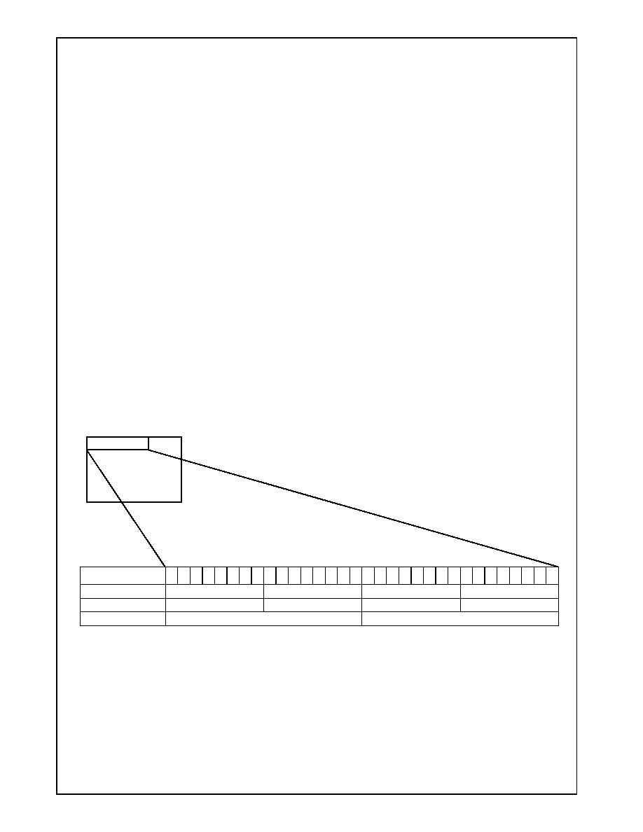
Revision 3.1
135
www.national.com
Integrated Functions (
Continued
)
GeodeTM
G
Xm
P
r
ocessor
4.5.8
Graphics Memory Map
The GXm processor supports a maximum of 4 MB of
graphics memory and will map it to an address space (see
Figure 4-2 on page 93) higher than the maximum amount
of installed RAM. The graphics memory aperture physi-
cally resides at the top of the installed system RAM. The
start address and size of the graphics memory aperture
are programmable on 128 KB boundaries. Typically, the
system BIOS sets the size and start address of the graph-
ics memory aperture during the boot process based on
the amount of installed RAM, user defined CMOS set-
tings, and display resolution. The graphics pipeline and
display controller address the graphics memory with a 20-
bit offset (address bits [21:2]) and four byte enables into
the graphics memory aperture. The graphics memory
stores several buffers that are used to generate the dis-
play: the frame buffer, compressed display buffer, VGA
memory, and cursor pattern(s). Any remaining off-screen
memory within the graphics aperture may be used by the
display driver as desired or not at all.
4.5.8.1
DC Memory Organization Registers
The display controller contains a number of registers that
allow full programmability of the graphics memory organi-
zation. This includes starting offsets for each of the buffer
regions described above, line delta parameters for the
frame buffer and compression buffer, as well as com-
pressed line-buffer size information. The starting offsets
for the various buffers are programmable for a high
degree of flexibility in memory organization.
4.5.8.2
Frame Buffer and Compression Buffer
Organization
The GXm processor supports primary display modes
640x480, 800x600, and 1024x768 at both 8 BPP and 16
BPP, and 1280x1024 at 8 BPP. Pixels will be packed into
DWORDs as shown in Figure 4-15.
In order to simplify address calculations by the rendering
hardware, the frame buffer is organized in an XY fashion
where the offset is simply a concatenation of the X and Y
pixel addresses. All 8 BPP display modes with the excep-
tion of 1280x1024 resolution will use a 1024-byte line
delta between the starting offsets of adjacent lines. All 16
BPP display modes and 1280x1024x8 BPP display
modes will use a 2048-byte line delta between the starting
offsets of adjacent lines. If there is room, the space
between the end of a line and the start of the next line will
be filled with the compressed display data for that line,
thus allowing efficient memory utilization. For 1024x768
display modes, the frame-buffer line size is the same as
the line delta, so no room is left for the compressed dis-
play data between lines. In this case, the compressed dis-
play buffer begins at the end of the frame buffer region
and is linearly mapped.
Figure 4-15. Pixel Arrangement Within a DWORD
Bit Position
31 30 29 28 27 26 25 24 23 22 21 20 19 18 17 16 15 14 13 12 11 10 9
8 7
6 5
4 3 2
1 0
Address
3h
2h
1h
0h
Pixel Org - 8 BPP
(3,0)
(2,0)
(1,0)
(0,0)
Pixel Org - 16 BPP
(1,0)
(0,0)
(1023,0)
(1023, 1023)
(0, 0)
(0, 1023)
DWORD 0
www.national.com
136
Revision 3.1
Integrated Functions (
Continued
)
GeodeTM
G
Xm
Pr
ocessor
4.5.8.3
VGA Display Support
The graphics pipeline contains full hardware support for
the VGA front end. The VGA data is stored in a 256 KB
buffer located in graphics memory. The main task for Soft-
VGA is converting the data in the VGA buffer to an 8 BPP
frame buffer that can be displayed by the GXm proces-
sor's hardware.
For some modes, the display controller can display the
VGA data directly and the data conversion is not neces-
sary. This includes standard VGA mode 13h and the vari-
ations of that mode used in several games; the display
controller can also directly display VGA planar graphics
modes D, E, F, 10, 11, and 12. Likewise, the hardware can
directly display all of the higher-resolution VESA modes.
Since the frame buffer data is written directly to memory
instead of travelling across an external bus, the GXm pro-
cessor outperforms typical VGA cards for these modes.
The display controller, however, does not directly support
text modes. SoftVGA must then convert the characters
and attributes in the VGA buffer to an 8 BPP frame buffer
the hardware uses for display refresh. See Section 4 "Vir-
tual Subsystem Architecture" for SoftVGA details.
4.5.8.4
Cursor Pattern Memory Organization
The cursor overlay patterns are loaded to independent
memory locations, usually mapped above the frame buffer
and compressed display buffer (off-screen). The cursor
buffer must start on a 16-byte aligned boundary. It is lin-
early mapped, and is always 256 bytes in size. If there is
enough room (256 bytes) after the compression-buffer line
but before the next frame-buffer line starts, the cursor pat-
tern may be loaded into this area to make efficient use of
the graphics memory.
Each pattern is a 32x32-pixel array of 2-bit codes. The
codes are a combination of AND mask and XOR mask for
a particular pixel. Each line of an overlay pattern is stored
as two DWORDs, with each DWORD containing the AND
masks for 16 pixels in the upper word and the XOR masks
for 16 pixels in the lower word. DWORDs are arranged
with the leftmost pixel block being least significant and the
rightmost pixel block being most significant. Pixels within
words are arranged with the leftmost pixels being most
significant and the rightmost pixels being least significant.
Multiple cursor patterns may be loaded into the off-screen
memory. An application may simply change the cursor
start offset to select a new cursor pattern. The new cursor
pattern will be used at the start of the next frame scan.
4.5.9
Display Controller Registers
The Display Controller maps 100h locations starting at
GX_BASE+8300h. Refer to Section 4.1.2 "Control Regis-
ters" on page 94 for instructions on accessing these regis-
ters.
The Display Controller Registers are divided into six cate-
gories:
∑ Configuration and Status Registers
∑ Memory Organization Registers
∑ Timing Registers
∑ Cursor and Line Compare Registers
∑ Color Registers
∑ Palette and RAM Diagnostic Registers
Table 4-29 summarizes these registers and locations and
the following subsections give detailed register/bit for-
mats.
Table 4-29. Display Controller Register Summary
GX_BASE+
Memory Offset
Type
Name/Function
Default
Value
Configuration and Status Registers
8300h-8303h
R/W
DC_UNLOCK
Display Controller Unlock -- This register is provided to lock the most critical memory-
mapped display controller registers to prevent unwanted modification (write operations).
Read operations are always allowed.
00000000h
8304h-8307h
R/W
DC_GENERAL_CFG
Display Controller General Configuration -- General control bits for the display controller.
00000000h
8308h-830Bh
R/W
DC_TIMING_CFG
Display Controller Timing Configuration -- Status and control bits for various display
timing functions.
xx000000h
830Ch-830Fh
R/W
DC_OUTPUT_CFG
Display Controller Output Configuration -- Status and control bits for pixel output
formatting functions.
xx000000h
Memory Organization Registers
8310h-8313h
R/W
DC_FB_ST_OFFSET
Display Controller Frame Buffer Start Address -- Specifies offset at which the frame buffer
starts.
xxxxxxxxh

Revision 3.1
137
www.national.com
Integrated Functions (
Continued
)
GeodeTM
G
Xm
P
r
ocessor
8314h-8317h
R/W
DC_CB_ST_OFFSET
Display Controller Compression Buffer Start Address -- Specifies offset at which the com-
pressed display buffer starts.
xxxxxxxxh
8318h-831Bh
R/W
DC_CURS_ST_OFFSET
Display Controller Cursor Buffer Start Address -- Specifies offset at which the cursor mem-
ory buffer starts.
xxxxxxxxh
831Ch-831Fh
--
Reserved
00000000h
8320h-8323h
R/W
DC_VID_ST_OFFSET
Display Controller Video Start Address -- Specifies offset at which the video buffer starts.
xxxxxxxxh
8324h-8327h
R/W
DC_LINE_DELTA
Display Controller Line Delta -- Stores line delta for the graphics display buffers.
xxxxxxxxh
8328h-832Bh
R/W
DC_BUF_SIZE
Display Controller Buffer Size -- Specifies the number of bytes to transfer for a line of
frame buffer data and the size of the compressed line buffer.
xxxxxxxxh
832Ch-832Fh
--
Reserved
00000000h
Timing Registers
8330h-8333h
R/W
DC_H_TIMING_1
Display Controller Horizontal and Total Timing -- Horizontal active and total timing
information.
xxxxxxxxh
8334h-8337h
R/W
DC_H_TIMING_2
Display Controller CRT Horizontal Blanking Timing -- CRT horizontal blank timing
information.
xxxxxxxxh
8338h-833Bh
R/W
DC_H_TIMING_3
Display Controller CRT Sync Timing -- CRT horizontal sync timing information.
xxxxxxxxh
833Ch-833Fh
R/W
DC_FP_H_TIMING
Display Controller Flat Panel Horizontal Sync Timing: Horizontal sync timing information for
an attached flat panel display.
xxxxxxxxh
8340h-8343h
R/W
DC_V_TIMING_1
Display Controller Vertical and Total Timing -- Vertical active and total timing information.
The parameters pertain to both CRT and flat panel display.
xxxxxxxxh
8344h-8247h
R/W
DC_V_TIMING_2
Display Controller CRT Vertical Blank Timing -- Vertical blank timing information.
xxxxxxxxh
8348h-834Bh
R/W
DC_V_TIMING_3
Display Controller CRT Vertical Sync Timing -- CRT vertical sync timing information.
xxxxxxxxh
834Ch-834Fh
R/W
DC_FP_V_TIMING
Display Controller Flat Panel Vertical Sync Timing -- Flat panel vertical sync timing
information.
xxxxxxxxh
Cursor and Line Compare Registers
8350h-8353h
R/W
DC_CURSOR_X
Display Controller Cursor X Position -- X position information of the hardware cursor.
xxxxxxxxh
8354h-8357h
RO
DC_V_LINE_CNT
Display Controller Vertical Line Count -- This read only register provides the current scan-
line for the display. It is used by software to time update of the frame buffer to avoid tearing
artifacts.
xxxxxxxxh
8358h-835Bh
R/W
DC_CURSOR_Y
Display Controller Cursor Y Position -- Y position information of the hardware cursor.
xxxxxxxxh
835Ch-835Fh
R/W
DC_SS_LINE_CMP
Display Controller Split-Screen Line Compare -- Contains the line count at which the lower
screen begins in a VGA split-screen mode.
xxxxxxxxh
Table 4-29. Display Controller Register Summary (Continued)
GX_BASE+
Memory Offset
Type
Name/Function
Default
Value
www.national.com
138
Revision 3.1
Integrated Functions (
Continued
)
GeodeTM
G
Xm
Pr
ocessor
Color Registers
8360h-8363h
R/W
DC_CURSOR_COLOR
Display Controller Cursor Color -- Contains the 8-bit indices for the cursor colors.
xxxxxxxxh
8364h-8367h
--
Reserved
00000000h
8368h-836Bh
R/W
DC_BORDER_COLOR
Display Controller Border Color -- Contains the 8-bit index for the border or overscan color.
xxxxxxxxh
836Ch-836Fh
--
Reserved
00000000h
Palette and RAM Diagnostic Registers
8370h-8373h
R/W
DC_PAL_ADDRESS
Display Controller Palette Address -- This register should be written with the address
(index) location to be used for the next access to the DC_PAL_DATA register.
xxxxxxxxh
8374h-8377h
R/W
DC_PAL_DATA
Display Controller Palette Data -- Contains the data for a palette access cycle.
xxxxxxxxh
8378h-837Bh
R/W
DC_DFIFO_DIAG
Display Controller Display FIFO Diagnostic -- This register is provided to enable testability
of the Display FIFO RAM.
xxxxxxxxh
837Ch-837Fh
R/W
DC_CFIFO_DIAG
Display Controller Compression FIFO Diagnostic -- This register is provided to enable test-
ability of the Compressed Line Buffer (FIFO) RAM.
xxxxxxxxh
Table 4-29. Display Controller Register Summary (Continued)
GX_BASE+
Memory Offset
Type
Name/Function
Default
Value
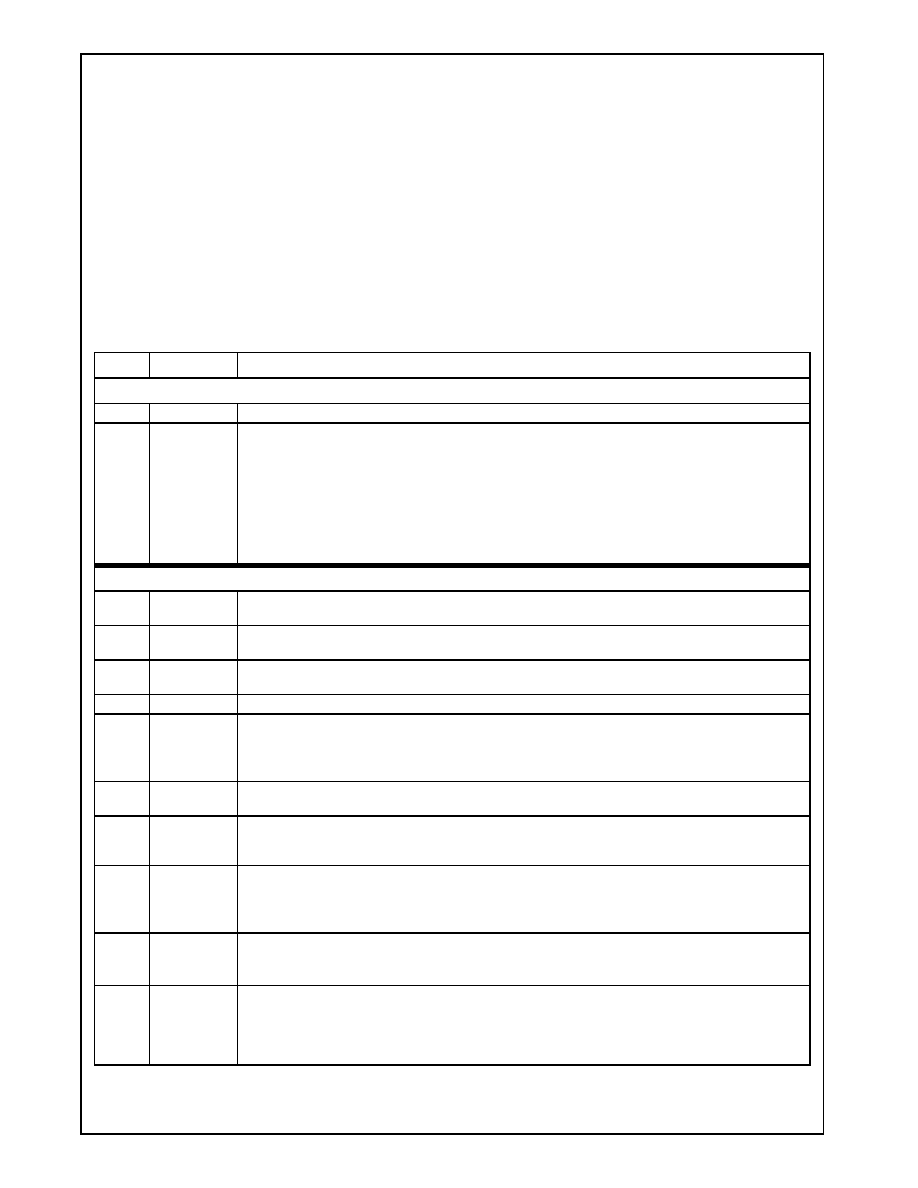
Revision 3.1
139
www.national.com
Integrated Functions (
Continued
)
GeodeTM
G
Xm
P
r
ocessor
4.5.9.1
Configuration and Status Registers
The Configuration and Status Registers group consists of
four 32-bit registers located at GX_BASE+8300h-830Ch.
These registers are described below and Table 4-30 gives
their bit formats.
∑ Display Controller Unlock (DC_UNLOCK)
- This register is provided to lock the most critical
memory-mapped display controller registers to
prevent unwanted modification (write operations).
Read operations are always allowed.
∑ Display Controller General Configuration
(DC_GENERAL_CFG)
- General control bits for the display controller.
∑ Display Controller Timing Configuration
(DC_TIMING_CFG)
- Status and control bits for various display timing
functions.
∑ Display Controller Output Configuration
(DC_OUTPUT_CFG)
- Status and control bits for pixel output formatting
functions.
Table 4-30. Display Controller Configuration and Status Registers
Bit
Name
Description
GX_BASE+8300h-8303h
DC_UNLOCK Register (R/W)
Default Value = 00000000h
31:16
RSVD
Reserved: Set to 0.
15:0
UNLOCK_
CODE
Unlock Code: This register must be written with the value 4758h in order to write to the protected regis-
ters. The following registers are protected by the locking mechanism.
DC_GENERAL_CFG
DC_CB_ST_OFFSET,
DC_BUF_SIZE,
DC_V_TIMING_2
DC_TIMING_CFG,
DC_CURS_ST_OFFSET,
DC_H_TIMING_1,
DC_V_TIMING_3
DC_OUTPUT_CFG,
DC_H_TIMNG_2,
DC_FP_H_TIMING
DC_FB_ST_OFFSET,
DC_LINE_DELTA,
DC_FP_V_TIMING
GX_BASE+8304h-8307h
DC_GENERAL_CFG (R/W)
Default Value = 00000000h
31
DDCK
Divide Dot Clock: Divide internal DOTCLK by two relative to PCLK (pertains only to 16 BPP display
modes utilizing an eight-bit RAMDAC): 0 = Disable; 1 = Enable.
30
DPCK
Divide Pixel Clock: Divide PCLK by two relative to internal DOTCLK (pertains only to display modes that
pack two pixels together such as 1280x1024 on an external CRT only): 0 = Disable; 1 = Enable.
29
VRDY
Video Ready Protocol: 0 = Low speed video port, use with V2.3 and older.
1 = High speed video port, use with V2.4 and newer.
28
VIDE
Video Enable: Motion video port: 0 = Disable; 1 = Enable.
27
SSLC
Split-screen Line Compare: VGA line compare function: 0 = Disable; 1 = Enable.
When enabled, the internal line counter will be compared to the value programmed in the DC_SS
_LINE_CMP register. If it matches, the frame buffer address will be reset to zero. This enables a split
screen function.
26
CH4S
Chain 4 Skip: Allow display controller to read every 4th DWORD from the frame buffer for compatibility
with the VGA: 0 = Disable; 1 = Enable.
25
DIAG
FIFO Diagnostic Mode: This bit allows testability of the on-chip Display FIFO and Compressed Line
Buffer via the diagnostic access registers. A low-to-high transition will reset the Display FIFO's R/W point-
ers and the Compressed Line Buffer's read pointer. 0 = Normal operation; 1 = Enable.
24
LDBL
Line Double: Allow line doubling for emulated VGA modes: 0 = Disable; 1 = Enable.
If enabled, this will cause each odd line to be replicated from the previous line as the data is sent to the dis-
play. Timing parameters should be programmed as if no pixel doubling is used, however, the frame buffer
should be loaded with half the normal number of lines.
23
CKWR
Clock Write: This bit will be output directly to an external clock chip or SYNDAC. The bit should be pulsed
high and low by the software to strobe data into the chip.
Note that this bit can be used in conjunction with the DACRS[2:0] pins.
22:20
DAC_RS[2:0]
RAMDAC Register Selects: This 3-bit field sets the register select inputs to the external RAMDAC for the
next cycle. It is used to allow access to the extended register set of the RAMDAC. Alternatively, these bits
may be used in selecting the frequency for an external clock chip or SYNDAC. If more than eight frequency
selections are required, the RAMDAC extended register programming sequence must be used or the addi-
tional select bit must be provided by some other means.

www.national.com
140
Revision 3.1
Integrated Functions (
Continued
)
GeodeTM
G
Xm
Pr
ocessor
19
RTPM
Real-Time Performance Monitoring: Allows real-time monitoring of a variety of internal GXm
processor signals by multiplexing the signals onto the CLKWR and DACRS[2:0] pins:
0 = Disable (Normal operation); 1 = Enable.
The CLKWR pin should not be fed to a clock chip or SYNDAC when this mode of operation is used, a dif-
ferent programming scheme should be used for the clock chip using the DACRS[2:0] signals and RAM-
DACRD# and RAMDACWR# signals. The selection of output signals is made using bits [27:16] of the
DC_BUF_SIZE register. The lower 12 bits of this field will select one of eight outputs for each pin.
18
FDTY
Frame Dirty Mode: Allow entire frame to be flagged as dirty whenever a pixel write occurs to the frame
buffer (this is provided for modes that use a linearly mapped frame buffer for which the line delta is not
equal to 1024 or 2048 bytes): 0 = Disable; 1 = Enable.
When disabled, dirty bits are set according to the Y address of the pixel write.
17
RSVD
Reserved: Set to 0.
16
CMPI
Compressor Insert Mode: Insert one static frame between update frames: 0 = Disable; 1 = Enable.
An update frame is referred to as a frame in which dirty lines will be allowed to be updated. Conversely, a
static frame is referred to as a frame in which dirty lines will not be updated (although the image may not
be static, since lines that are not compressed successfully must be retrieved from the uncompressed
frame buffer).
15:12
DFIFO
HI-PRI END
LVL
Display FIFO High Priority End Level: This field specifies the depth of the display FIFO (in 64-bit entries
x 4) at which a high-priority request previously issued to the memory controller will end. The value is
dependent upon display mode.
This register should always be non-zero and should be larger than the start level.
11:8
DFIFO
HI-PRI
START LVL
Display FIFO High Priority Start Level: This field specifies the depth of the display FIFO (in 64-bit entries
x 4) at which a high-priority request will be sent to the memory controller to fill up the FIFO. The value is
dependent upon display mode.
This register should always be nonzero and should be less than the high-priority end level.
7:6
DCLK_
MUL
DCLK Multiplier: This 2-bit field specifies the clock multiplier for the input DCLK pin. After the input clock
is optionally multiplied, the internal DOTCLK, PCLK, and FPCLK may be divided as necessary.
00 = Forced Low
01 = 1 x DCLK
10 = 2 x DCLK
11 = 4 x DCLK
5
DECE
Decompression Enable: Allow operation of internal decompression hardware:
0 = Disable; 1 = Enable.
4
CMPE
Compression Enable: Allow operation of internal compression hardware: 0 = Disable; 1 = Enable
3
PPC
Pixel Panning Compatibility: This bit has the same function as that found in the VGA.
Allow pixel alignment to change when crossing a split-screen boundary - it will force the pixel alignment to
be 16-byte aligned: 0 = Disable; 1 = Enable.
If disabled, the previous alignment will be preserved when crossing a split-screen boundary.
2
DVCK
Divide Video Clock: Selects frequency of VID_CLK pin:
0 = VID_CLK pin frequency is equal to one-half (Ω) the frequency of the core clock.
1 = VID_CLK pin frequency is equal to one-fourth (º) the frequency of the core clock.
Note: Bit 28 (VIDE) must be set to 1 for this bit to be valid.
1
CURE
Cursor Enable: Allow operation of internal hardware cursor: 0 = Disable; 1 = Enable.
0
DFLE
Display FIFO Load Enable: Allow the display FIFO to be loaded from memory:
0 = Disable; 1 = Enable.
If disabled, no write or read operations will occur to the display FIFO.
If enabled, a flat panel should be powered down prior to setting this bit low. Similarly, if active, a CRT
should be blanked prior to setting this bit low.
Table 4-30. Display Controller Configuration and Status Registers (Continued)
Bit
Name
Description

Revision 3.1
141
www.national.com
Integrated Functions (
Continued
)
GeodeTM
G
Xm
P
r
ocessor
GX_BASE+8308h-830Bh
DC_TIMING_CFG Register (R/W)
Default Value = xxx00000h
31
VINT
(RO)
Vertical Interrupt (Read Only): Is a vertical interrupt pending? 0 = No; 1 = Yes.
This bit is provided to maintain backward compatibility with the VGA. It corresponds to VGA port 3C2h bit
7.
30
VNA
(RO)
Vertical Not Active (Read Only): Is the active part of a vertical scan is in progress (i.e. retrace, blanking,
or border)? 0 = Yes; 1 = No.
This bit is provided to maintain backward compatibility with the VGA. It corresponds to VGA port 3BA/3DA
bit 3.
29
DNA
(RO)
Display Not Active (Read Only): Is the active part of a line is being displayed (i.e. retrace, blanking, or
border)? 0 = Yes; 1 = No.
This bit is provided to maintain backward compatibility with the VGA. It corresponds to VGA port 3BA/3DA
bit 0.
28
SENS
(RO)
Monitor Sense (Read Only): This bit returns the result of the voltage comparator test of the RGB lines
from the external RAMDAC. The value will be a low level if one or more of the comparators exceed the 340
mV level indicating an unloaded line.
This bit can be tested repeatedly to determine the loading on the red, green, and blue lines by loading the
palette with various values. The BIOS can then determine whether a color, monochrome, or no monitor is
attached. If no RAMDAC is attached, the BIOS should assume that a color panel is attached and operate
in color mode. For VGA emulation, read operations to port 3C2 bit 4 are redirected here.
27
DDCI
(RO)
DDC Input (Read Only): This bit returns the value from the DDCIN pin that should reflect the value from
pin 12 of the VGA connector. It is used to provide support for the VESA Display Data Channel standard
level DDC1.
26:20
RSVD
Reserved: Set to 0.
19:17
PWR_SEQ
DELAY
Power Sequence Delay: This 3-bit field sets the delay between edges for the power sequencing control
logic. The actual delay is this value multiplied by one frame period (typically 16ms).
Note that a value of zero will result in a delay of only one DOTCLK period.
16
BKRT
Blink Rate:
0 = Cursor blinks on every 16 frames for a duration of 8 frames (approximately 4 times per second) and
VGA text characters will blink on every 32 frames for a duration of 16 frames (approximately 2 times per
second).
1 = Cursor blinks on every 32 frames for a duration of 16 frames (approximately 2 times per second) and
VGA text characters blink on every 64 frames for a duration of 32 frames (approximately 1 time per sec-
ond).
15
PXDB
Pixel Double: Allow pixel doubling to stretch the displayed image in the horizontal dimension:
0 = Disable; 1 = Enable.
If bit 15 is enabled, timing parameters should be programmed as if no pixel doubling is used, however, the
frame buffer should be loaded with half the normal pixels per line. Also, the FB_LINE_SIZE parameter in
DC_BUF_SIZE should be set for the number of bytes to be transferred for the line rather than the number
displayed.
14
INTL
Interlace Scan: Allow interlaced scan mode:
0 = Disable (non-interlaced scanning is supported)
1 = Enable (If a flat panel is attached, it should be powered down before setting this bit.)
13
PLNR
VGA Planar Mode: This bit must be set high for all VGA planar display modes.
12
FCEN
Flat Panel Center: Allows the border and active portions of a scan line to be qualified as "active" to a flat
panel display via the ENADISP signal. This allows the use of a large border region for centering the flat
panel display. 0 = Disable; 1 = Enable.
When disabled, only the normal active portion of the scan line will be qualified as active.
11
FVSP
Flat Panel Vertical Sync Polarity:
0 = Causes TFT vertical sync signal to be normally low, generating a high pulse during sync interval.
1 = Causes TFT vertical sync signal to be normally high, generating a low pulse during sync interval.
10
FHSP
Flat Panel Horizontal Sync Polarity:
0 = Causes TFT horizontal sync signal to be normally low, generating a high pulse during sync interval.
1 = Causes TFT horizontal sync signal to be normally high, generating a low pulse during sync interval.
Table 4-30. Display Controller Configuration and Status Registers (Continued)
Bit
Name
Description

www.national.com
142
Revision 3.1
Integrated Functions (
Continued
)
GeodeTM
G
Xm
Pr
ocessor
9
CVSP
CRT Vertical Sync Polarity:
0 = Causes CRT VSYNC signal to be normally low, generating a high pulse during the retrace interval.
1 = Cause CRT VSYNC signal to be normally high, generating a low pulse during the retrace interval.
8
CHSP
CRT Horizontal Sync Polarity:
0 = Causes CRT HSYNC signal to be normally low, generating a high pulse during the retrace interval.
1 = Causes CRT HSYNC signal to be normally high, generating a low pulse during the retrace interval.
7
BLNK
Blink Enable: Blink circuitry: 0 = Disable; 1 = Enable.
If enabled, the hardware cursor will blink as well as any pixels. This is provided to maintain compatibility
with VGA text modes. The blink rate is determined by the bit 16 (BKRT).
6
VIEN
Vertical Interrupt Enable: Generate a vertical interrupt on the occurrence of the next vertical sync pulse:
0 = Disable, vertical interrupt is cleared;
1 = Enable.
This bit is provided to maintain backward compatibility with the VGA.
5
TGEN
Timing Generator Enable: Allow timing generator to generate the timing control signals for the display.
0 = Disable, the Timing Registers may be reprogrammed, and all circuitry operating on the DOTCLK will be
reset.
1 = Enable, no write operations are permitted to the Timing Registers.
4
DDCK
DDC Clock: This bit is used to provide the serial clock for reading the DDC data pin. This bit is multiplexed
onto the CRTVSYNC pin, but in order for it to have an effect, the VSYE bit must be set low to disable the
normal vertical sync. Software should then pulse this bit high and low to clock data into the GXm proces-
sor.
This feature is provided to allow support for the VESA Display Data Channel standard level DDC1.
3
BLKE
Blank Enable: Allow generation of the composite blank signal to the display device:
0 = Disable; 1 = Enable.
When disabled, the BLANK# output will be a static low level. This allows VESA DPMS compliance.
2
VSYE
Horizontal Sync Enable: Allow generation of the horizontal sync signal to a CRT display device:
0 = Disable; 1 = Enable.
When disabled, the HSYNC output will be a static low level. This allows VESA DPMS compliance.
Note that this bit only applies to the CRT; the flat panel HSYNC is controlled by the automatic power
sequencing logic.
1
HSYE
Vertical Sync Enable: Allow generation of the vertical sync signal to a CRT display device:
0 = Disable; 1 = Enable.
When disabled, the VSYNC output will be a static low level. This allows VESA DPMS compliance.
Note that this bit only applies to the CRT; the flat panel VSYNC is controlled by the automatic power
sequencing logic.
0
FPPE
Flat Panel Power Enable: On a low-to-high transition this bit will enable the flat panel power-up sequence
to begin. This will first turn on VDD to the panel, then start the clocks, syncs, and pixel bus, then turn on
the LCD bias voltage, and finally the backlight.
On a high-to-low transition, this bit will disable the outputs in the reverse order.
GX_BASE+830Ch-830Fh
DC_OUTPUT_CFG Register (R/W)
Default Value = xxx00000h
31:16
RSVD
Reserved: Set to 0.
15
DIAG
Compressed Line Buffer Diagnostic Mode: This bit will allow testability of the Compressed Line Buffer
via the diagnostic access registers. A low-to-high transition will reset the Compressed Line Buffer write
pointer. 0 = Disable (Normal operation); 1 = Enable.
14
CFRW
Compressed Line Buffer Read/Write Select: Enables the read/write address to the Compressed Line
Buffer for use in diagnostic testing of the RAM.
0 = Write address enabled
1 = Read address enabled
13
PDEH
Panel Data Enable High:
0 = The PANEL[17:9] data bus to be driven to a logic low level to effectively blank an attached flat panel
display or disable the upper pixel data bus for 16-bit pixel port RAMDACs.
1 = If no flat panel is attached, the PANEL[17:9] data bus will be driven with active pixel data. If a flat panel
is attached, setting this bit high will have no effect
-
the upper panel bus will be driven based upon the
power sequencing logic.
Table 4-30. Display Controller Configuration and Status Registers (Continued)
Bit
Name
Description

Revision 3.1
143
www.national.com
Integrated Functions (
Continued
)
GeodeTM
G
Xm
P
r
ocessor
12
PDEL
Panel Data Enable Low:
0 = This bit will cause the PANEL[8:0] data bus to be driven to a logic low level to effectively blank an
attached flat panel display or disable the lower panel data bus if it is not required.
1= If no flat panel is attached, the PANEL[8:0] data bus will be driven with active pixel data. If a flat panel is
attached, setting this bit high will have no effect
-
the lower panel bus will be driven based upon the power
sequencing logic.
11
PRMP
Palette Re-map:
0 = The modified codes are sent to the RAMDAC and the external palette should uses the modified map-
ping.
1 = Bits [8:1] of the palette output register are routed to the RAMDAC data bus. The GXm processor inter-
nal palette RAM may be loaded with 8-bit VGA indices to translate the modified codes stored in display
memory so that the RAMDAC data bus will contain the expected indices. The modified codes are used to
achieve character blinking in VGA text modes. This mode should be set high set high only for desktop sys-
tems with no flat panel attached. It should only be necessary when 8514/A or VESA standard feature con-
nector support is required.
10
CKSL
Clock Select: Selects output used to clock PANEL[17:0], FPHSYNC, FPVSYNC, and ENADISP output
pins.
1 = PCLK
0 = FPCLK (based upon the power sequencing logic)
This bit should be high when using a 16-bit RAMDAC.
9
FRMS
Frame Rate Modulation Select:
0 = Enables FRM circuitry to change the pattern displayed every frame.
1 = Enables FRM circuitry to change the pattern displayed every two frames (to allow for slower response
time liquid crystal materials).
8
3/4ADD
3- or 4-bit Add:
0 = Enables dither and FRM circuitry to operate on the 3 most significant bits of each color component for
9-bit TFT panels.
1 = Enables the dither and FRM circuitry to operate on the 4 most significant bits of each color component
for 12-bit TFT panels.
7
RSVD
Reserved: Must be set to 0.
6
RSVD
Reserved: Must be set to 0.
5
RSVD
Reserved: Must be set to 0.
4
DITE
Dither Enable: Allow a 2x2 spatial dither on the 3-bit or 4-bit color value. Note that dither will not be sup-
ported for 12-bit TFT panels when FRM is enabled. 0 = Disable; 1 = Enable.
3
FRME
Frame-Rate Modulation Enable: Allow FRM to be performed on the 3-bit or 4-bit color value using the
next most significant bit after the least significant bit sent to the panel.
0 = Disable (no FRM performed);
1 = Enable.
2
PCKE
PCLK Enable:
0 = PCLK is disabled and a low logic level is driven off-chip. Also, the RAMDAC data bus is driven low.
1 = Enable PCLK to be driven off-chip.
This clock operates the RAMDAC interface.
1
16FMT
16 BPP Format: Selects RGB display mode:
0 = RGB 5-6-5 mode
1 = RGB 5-5-5 display mode
This bit is only significant if 8 BPP is low, indicating 16 BPP mode.
0
8BPP
8 BPP / 16 BPP Select:
0 = 16-bit per pixel display mode is selected. (Bit 1 of OUTPUT_CONFIG will indicate the format of the 16
bit data.)
1 = 8-bit-per-pixel display mode is selected. This is the also the mode used in VGA emulation.
Table 4-30. Display Controller Configuration and Status Registers (Continued)
Bit
Name
Description

www.national.com
144
Revision 3.1
Integrated Functions (
Continued
)
GeodeTM
G
Xm
Pr
ocessor
4.5.10 Memory Organization Registers
The GXm processor utilizes a graphics memory aperture
that is up to 4 MB in size. The base address of the graph-
ics memory aperture is stored in the DRAM controller.
The graphics memory is made up of the normal uncom-
pressed frame buffer, compressed display buffer, and cur-
sor buffer. Each buffer begins at a programmable offset
within the graphics memory aperture.
The various memory buffers are arranged so as to effi-
ciently pack the data within the graphics memory aper-
ture. This requires flexibility in the way that the buffers are
arranged when different display modes are in use. The
cursor buffer is a linear block so addressing is straightfor-
ward. The frame buffer and compressed display buffer are
arranged based upon scan lines. Each scan line has a
maximum number of valid or active DWORDs and a delta,
that when added to the previous line offset, points to the
next line. In this way, the buffers may be stored as linear
blocks or as logical blocks as may be desired.
The Memory Organization Registers group consists of six
32-bit
registers
located
at
GX_BASE+8310h-8328h.
These registers are described below and Table 4-31 gives
their bit formats.
∑ Display Controller Frame Buffer Start Address
(DC_FB_ST_OFFSET)
- Specifies the offset at which the frame buffer starts.
∑ Display Controller Compression Buffer Start Address
(DC_CB_ST_OFFSET)
- Specifies the offset at which the compressed display
buffer starts.
∑ Display Controller Cursor Buffer Start Address
(DC_CURS_ST_OFFSET)
- Specifies the offset at which the cursor memory
buffer starts.
∑ Display Controller Video Start Address
(DC_VID_ST_OFFSET)
- Specifies the offset at which the video buffer starts.
∑ Display Controller Line Delta (DC_LINE_DELTA)
- Stores the line delta for the graphics display buffers.
∑ Display Controller Buffer Size (DC_BUF_SIZE)
- Specifies the number of bytes to transfer for a line of
frame buffer data and the size of the compressed
line buffer. (The compressed line buffer will be invali-
dated if it exceeds the CB_LINE_SIZE, bits [15:9].)
Table 4-31. Display Controller Memory Organization Registers
Bit
Name
Description
GX_BASE+8310h-8313h
DC_FB_ST_OFFSET Register (R/W)
Default Value = xxxxxxxxh
31:22
RSVD
Reserved: Set to 0.
21:0
FB_START
_OFFSET
Frame Buffer Start Offset: This value represents the byte offset of the starting location of the displayed
frame buffer. This value may be changed to achieve panning across a virtual desktop or to allow multiple
buffering.
When this register is programmed to a nonzero value, the compression logic should be disabled. The
memory address defined by bits [21:4] will take effect at the start of the next frame scan. The pixel offset
defined by bits [3:0] will take effect immediately (in general, it should only change during vertical blank-
ing).
GX_BASE+8314h-8317h
DC_CB_ST_OFFSET Register (R/W)
Default Value = xxxxxxxxh
31:22
RSVD
Reserved: Set to 0.
21:0
CB_START
_OFFSET
Compressed Display Buffer Start Offset: This value represents the byte offset of the starting location
of the compressed display buffer. Bits [3:0] should always be programmed to zero so that the start offset
is aligned to a 16-byte boundary. This value should change only when a new display mode is set due to
a change in size of the frame buffer.
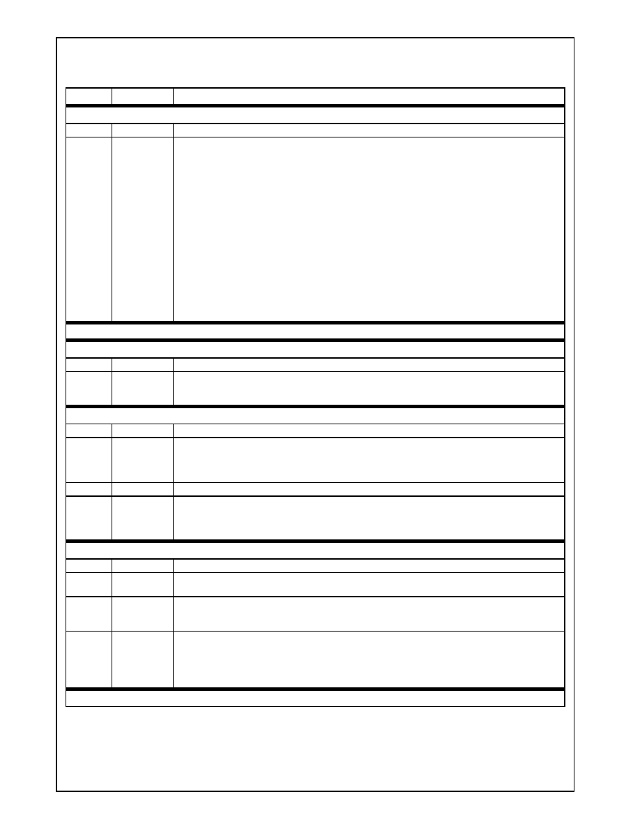
Revision 3.1
145
www.national.com
Integrated Functions (
Continued
)
GeodeTM
G
Xm
P
r
ocessor
GX_BASE+8318h-831Bh
DC_CUR_ST_OFFSET Register (R/W)
Default Value = xxxxxxxxh
31:22
RSVD
Reserved: Set to 0.
21:0
CUR_START
_OFFSET
Cursor Start Offset: This value represents the byte offset of the starting location of the cursor display
pattern. Bits [1:0] should always be programmed to zero so that the start offset is DWORD aligned. The
cursor data will be stored as a linear block of data. The active cursor will always be 32x32x2 bits in size.
Multiple cursor patterns may be loaded into off-screen memory. The start offset is loaded at the start of a
frame. Each cursor pattern will be exactly 256 bytes in size. Note that if there is a Y offset for the cursor
pattern, the cursor start offset should be set to point to the first displayed line of the cursor pattern. The
cursor code for a given pixel is determined by an AND mask and an XOR mask. Each line of a cursor will
be stored as two DWORDs, with each DWORD containing the AND masks for 16 pixels in the upper
word and the XOR masks for 16 pixels in the lower word. DWORDs will be arranged with the leftmost
block of 16 pixels being least significant and the rightmost block being most significant. Pixels within
words will be arranged with the leftmost pixels being most significant and the rightmost pixels being least
significant. The 2-bit cursor codes are as follows.
AND
XOR
Displayed
0
0
Cursor Color 0
0
1
Cursor Color 1
1
0
Transparent
-
Background Pixel
1
1
Inverted
-
Bit-wise Inversion of Background Pixel
GX_BASE+831Ch-831Fh
Reserved
Default Value = 00000000h
GX_BASE+8320h-8323h
DC_VID_ST_OFFSET Register (R/W)
Default Value = xxxxxxxxh
31:21
RSVD
Reserved: Set to 0.
20:0
VID_START
_OFFSET
Video Buffer Start Offset Value: This is the value for the Video Buffer Start Offset. It represents the
starting location for Video Buffer. Bits [3:0] should always be programmed as zero so that the start offset
is aligned to a 16 byte boundary.
GX_BASE+8324h-8327h
DC_LINE_DELTA Register (R/W)
Default Value = xxxxxxxxh
31:22
RSVD
Reserved: Set to 0.
21:12
CB_LINE_
DELTA
Compressed Display Buffer Line Delta: This value represents number of DWORDs that, when added
to the starting offset of the previous line, will point to the start of the next compressed line in memory. It
is used to always maintain a pointer to the starting offset for the compressed display buffer line being
loaded into the display FIFO.
11:10
RSVD
Reserved: Set to 0.
9:0
FB_LINE_
DELTA
Frame Buffer Line Delta: This value represents number of DWORDs that, when added to the starting
offset of the previous line, will point to the start of the next frame buffer line in memory. It is used to
always maintain a pointer to the starting offset for the frame buffer line being loaded into the display
FIFO.
GX_BASE+8328h-832Bh
DC_BUF_SIZE Register (R/W)
Default Value = xxxxxxxxh
31:30
RSVD
Reserved: Set to 0.
29:16
VID_BUF_
SIZE
Video Buffer Size: These bits set the video buffer size, in 64-byte segments. The maximum size is 1
MB.
15:9
CB_LINE_
SIZE
Compressed Display Buffer Line Size: This value represents the number of DWORDs for a valid com-
pressed line plus 1. It is used to detect an overflow of the compressed data FIFO. It should never be
larger than 41h or 65Dh since the maximum size of the compressed data FIFO is 64 DWORDs.
8:0
FB_LINE_
SIZE
Frame Buffer Line Size: This value specifies the number of QWORDS (8-byte segments) to transfer for
each display line from the frame buffer.
If panning is enabled, this value can generally be programmed to the displayed number of QWORDS + 2
so that enough data is transferred to handle any possible alignment. Extra pixel data in the FIFO at the
end of a line will automatically be discarded.
GX_BASE+832Ch-832Fh
Reserved
Default Value = 00000000h
Table 4-31. Display Controller Memory Organization Registers (Continued)
Bit
Name
Description

www.national.com
146
Revision 3.1
Integrated Functions (
Continued
)
GeodeTM
G
Xm
Pr
ocessor
4.5.11 Timing Registers
The GXm processor timing registers control the genera-
tion of sync, blanking, and active display regions. They
provide complete flexibility in interfacing to both CRT and
flat panel displays. These registers will generally be pro-
grammed by the BIOS from an INT 10h call or by the
extended mode driver from a display timing file. Note that
the horizontal timing parameters are specified in character
clocks, which actually means pixels divided by 8, since all
characters are bit mapped. For interlaced display the ver-
tical counter will be incremented twice during each display
line, so vertical timing parameters should be programmed
with reference to the total frame rather than a single field.
The Timing Registers group consists of six 32-bit registers
located at GX_BASE+8330h-834Ch. These registers are
described below and Table 4-32 gives their bit formats.
∑ Display Controller Horizontal and Total Timing
(DC_H_TIMING_1)
- Contains horizontal active and total timing informa-
tion.
∑ Display Controller CRT Horizontal Blanking Timing
(DC_H_TIMING_2 Register)
- Contains CRT horizontal blank timing information.
∑ Display Controller CRT Sync Timing
(DC_H_TIMING_3)
- Contains CRT horizontal sync timing information.
Note, however, that this register should also be
programmed appropriately for flat panel only display
since the horizontal sync transition determines when
to advance the vertical counter.
∑ Display Controller Flat Panel Horizontal Sync Timing
(DC_FP_H_TIMING)
- Contains horizontal sync timing information for an
attached flat panel display.
∑ Display Controller Vertical and Total Timing
(DC_V_TIMING_1)
- Contains vertical active and total timing information.
The parameters pertain to both CRT and flat panel
display.
∑ Display Controller CRT Vertical Blank Timing
(DC_V_TIMING_2)
- Contains vertical blank timing information.
∑ Display Controller CRT Vertical Sync Timing
(DC_V_TIMING_3)
- Contains CRT vertical sync timing information.
∑ Display Controller Flat Panel Vertical Sync Timing
(DC_FP_V_TIMING)
- Contains flat panel vertical sync timing information.
Table 4-32. Display Controller Timing Registers
Bit
Name
Description
GX_BASE+8330h-8333h
DC_H_TIMING_1 Register (R/W)
Default Value = xxxxxxxxh
31:27
RSVD
Reserved: Set to 0.
26:19
H_TOTAL
Horizontal Total: This field represents the total number of character clocks for a given scan line
minus 1. Note that the value is necessarily greater than the H_ACTIVE field because it includes bor-
der pixels and blanked pixels. For flat panels, this value will never change. The field [26:16] may be
programmed with the pixel count minus 1, although bits [18:16] are ignored. The horizontal total is
programmable on 8-pixel boundaries only.
18:16
RSVD
Reserved: These bits are readable and writable but have no effect.
15:11
RSVD
Reserved: Set to 0.
10:3
H_ACTIVE
Horizontal Active: This field represents the total number of character clocks for the displayed por-
tion of a scan line minus 1. The field [10:0] may be programmed with the pixel count minus 1,
although bits [2:0] are ignored. The active count is programmable on 8-pixel boundaries only. Note
that for flat panels, if this value is less than the panel active horizontal resolution (H_PANEL), the
parameters H_BLANK_START, H_BLANK_END, H_SYNC_START, and H_SYNC_END should be
reduced by the value of H_ADJUST (or the value of H_PANEL - H_ACTIVE / 2)to achieve horizontal
centering.
2:0
RSVD
Reserved: These bits are readable and writable but have no effect.
Note: Note also that for simultaneous CRT and flat panel display the H_ACTIVE and H_TOTAL parameters pertain to both.
GX_BASE+8334h-8337h
DC_H_TIMING_2 Register (R/W)
Default Value = xxxxxxxxh
31:27
RSVD
Reserved: Set to 0.
26:19
H_BLK_END
Horizontal Blank End: This field represents the character clock count at which the horizontal blank-
ing signal becomes inactive minus 1. The field [26:16] may be programmed with the pixel count
minus 1, although bits [18:16] are ignored. The blank end position is programmable on 8-pixel
boundaries only.
18:16
RSVD
Reserved: These bits are readable and writable but have no effect.
15:11
RSVD
Reserved: Set to 0.

Revision 3.1
147
www.national.com
Integrated Functions (
Continued
)
GeodeTM
G
Xm
P
r
ocessor
10:3
H_BLK_START
Horizontal Blank Start: This field represents the character clock count at which the horizontal
blanking signal becomes active minus 1. The field [10:0] may be programmed with the pixel count
minus 1, although bits [2:0] are ignored. The blank start position is programmable on 8-pixel bound-
aries only.
2:0
RSVD
Reserved: These bits are readable and writable but have no effect.
Note: A minimum of four character clocks is required for the horizontal blanking portion of a line in order for the timing generator to
function correctly.
GX_BASE+8338h-833Bh
DC_H_TIMING_3 Register (R/W)
Default Value = xxxxxxxxh
31:27
RSVD
Reserved: Set to 0.
26:19
H_SYNC_END
Horizontal Sync End: This field represents the character clock count at which the CRT horizontal
sync signal becomes inactive minus 1. The field [26:16] may be programmed with the pixel count
minus 1, although bits [18:16] are ignored. The sync end position is programmable on 8-pixel bound-
aries only.
18:16
RSVD
Reserved: These bits are readable and writable but have no effect.
15:11
RSVD
Reserved: Set to 0.
10:3
H_SYNC_START
Horizontal Sync Start: This field represents the character clock count at which the CRT horizontal
sync signal becomes active minus 1. The field [10:0] may be programmed with the pixel count minus
1, although bits [2:0] are ignored. The sync start position is programmable on 8-pixel boundaries
only.
2:0
RSVD
Reserved: These bits are readable and writable but have no effect.
Note: This register should also be programmed appropriately for flat panel only display since the horizontal sync transition deter-
mines when to advance the vertical counter.
GX_BASE+833Ch-833Fh
C_FP_H_TIMING Register (R/W)
Default Value = xxxxxxxxh
31:27
RSVD
Reserved: Set to 0.
26:16
FP_H_SYNC
_END
Flat Panel Horizontal Sync End: This field represents the pixel count at which the flat panel hori-
zontal sync signal becomes inactive minus 1.
15:11
RSVD
Reserved: Set to 0.
10:0
FP_H_SYNC
_START
Flat Panel Horizontal Sync Start: This field represents the pixel count at which the flat panel hori-
zontal sync signal becomes active minus 1.
Note: All values are specified in pixels rather than character clocks to allow precise control over sync position. Note, however, that for
flat panels which combine two pixels per panel clock, these values should be odd numbers (even pixel boundary) to guarantee
that the sync signal will meet proper setup and hold times.
GX_BASE+8340h-8343h
DC_V_TIMING_1 Register (R/W)
Default Value = xxxxxxxxh
31:27
RSVD
Reserved: Set to 0.
26:16
V_TOTAL
Vertical Total: This field represents the total number of lines for a given frame scan minus 1. Note
that the value is necessarily greater than the V_ACTIVE field because it includes border lines and
blanked lines. If the display is interlaced, the total number of lines must be odd, so this value should
be an even number.
15:11
RSVD
Reserved: Set to 0.
10:0
V_ACTIVE
Vertical Active: This field represents the total number of lines for the displayed portion of a frame
scan minus 1. Note that for flat panels, if this value is less than the panel active vertical resolution
(V_PANEL), the parameters V_BLANK_START, V_BLANK_END, V_SYNC_START, and
V_SYNC_END should be reduced by the following value (V_ADJUST) to achieve vertical centering:
V_ADJUST = (V_PANEL - V_ACTIVE) / 2
If the display is interlaced, the number of active lines should be even, so this value should be an odd
number.
Note: All values are specified in lines.
GX_BASE+8344h-8347h
DC_V_TIMING_2 Register (R/W)
Default Value = xxxxxxxxh
31:27
RSVD
Reserved: Set to 0.
26:16
V_BLANK_END
Vertical Blank End: This field represents the line at which the vertical blanking signal becomes
inactive minus 1. If the display is interlaced, no border is supported, so this value should be identical
to V_TOTAL.
15:11
RSVD
Reserved: Set to 0.
Table 4-32. Display Controller Timing Registers (Continued)
Bit
Name
Description
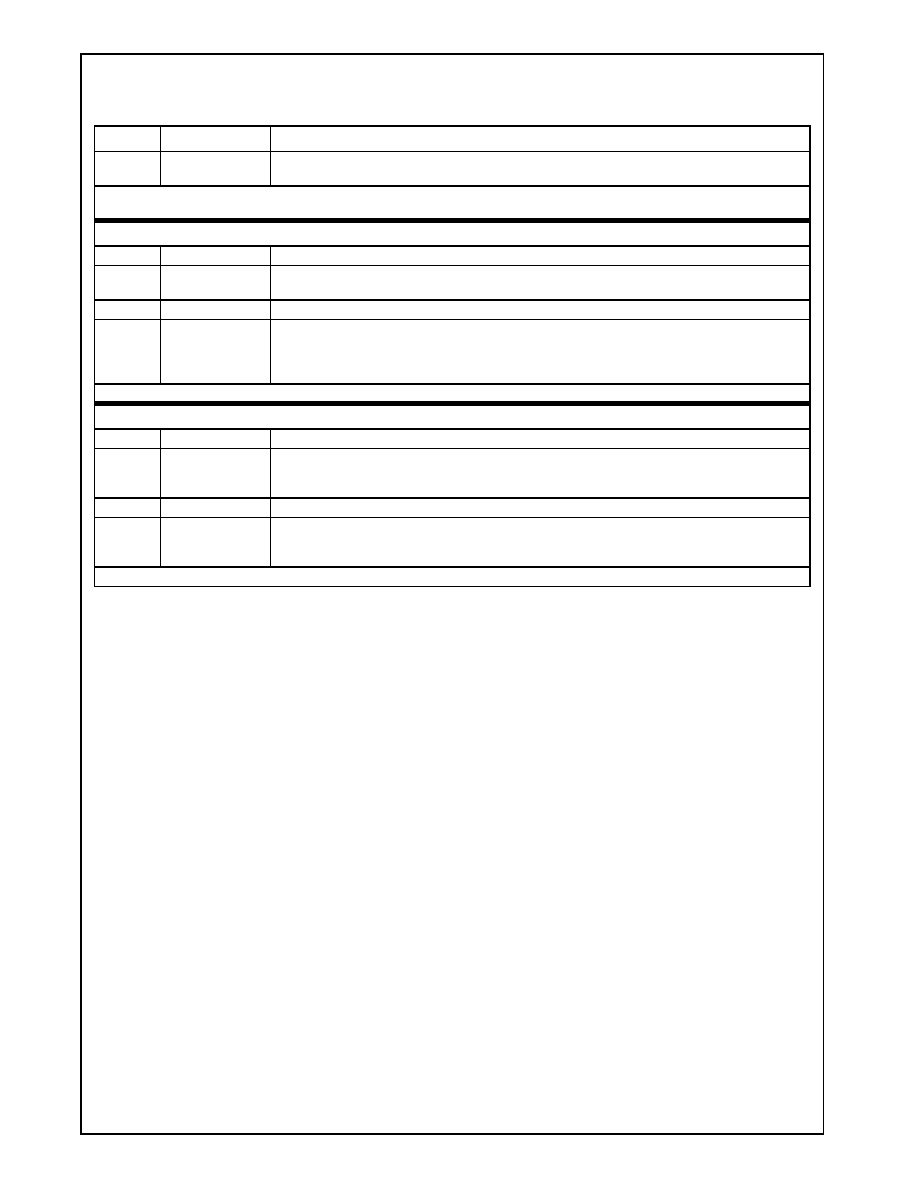
www.national.com
148
Revision 3.1
Integrated Functions (
Continued
)
GeodeTM
G
Xm
Pr
ocessor
10:0
V_BLANK_
START
Vertical Blank Start: This field represents the line at which the vertical blanking signal becomes
active minus 1. If the display is interlaced, this value should be programmed to V_ACTIVE plus 1.
Note: All values are specified in lines. For interlaced display, no border is supported, so blank timing is implied by the total/active tim-
ing.
GX_BASE+8348h-834Bh
DC_V_TIMING_3 Register (R/W)
Default Value = xxxxxxxxh
31:27
RSVD
Reserved: Set to 0.
26:16
V_SYNC_END
Vertical Sync End: This field represents the line at which the CRT vertical sync signal becomes
inactive minus 1.
15:11
RSVD
Reserved: Set to 0.
10:0
V_SYNC_START
Vertical Sync Start: This field represents the line at which the CRT vertical sync signal becomes
active minus 1. For interlaced display, note that the vertical counter is incremented twice during each
line and since there are an odd number of lines, the vertical sync pulse will trigger in the middle of a
line for one field and at the end of a line for the subsequent field.
Note: All values are specified in lines.
GX_BASE+834Ch-834Fh
DC_FP_V_TIMING Register (R/W)
Default Value = xxxxxxxxh
31:27
RSVD
Reserved: Set to 0.
26:16
FP_V_SYNC
_END
Flat Panel Vertical Sync End: This field represents the line at which the flat panel vertical sync sig-
nal becomes inactive minus 2. Note that the internal flat panel vertical sync is latched by the flat
panel horizontal sync prior to being output to the panel.
15:11
RSVD
Reserved: Set to 0.
10:0
FP_VSYNC
_START
Flat Panel Vertical Sync Start: This field represents the line at which the internal flat panel vertical
sync signal becomes active minus 2. Note that the internal flat panel vertical sync is latched by the
flat panel horizontal sync prior to being output to the panel.
Note: All values are specified in lines.
Table 4-32. Display Controller Timing Registers (Continued)
Bit
Name
Description
Revision 3.1
149
www.national.com
Integrated Functions (
Continued
)
GeodeTM
G
Xm
P
r
ocessor
4.5.12 Cursor Position Registers
The Cursor Position Registers contain pixel coordinate
information for the cursor. These values are not latched by
the timing generator until the start of the frame to avoid
tearing artifacts when moving the cursor.
The Cursor Position group consists of four 32-bit registers
located at GX_BASE+8350h-835Ch. These registers are
described below and Table 4-33 gives their bit formats.
∑ Display Controller Cursor X Position (DC_CURSOR_X)
- Contains the X position information of the hardware
cursor.
∑ Display Controller Vertical Line Count
(DC_V_LINE_CNT)
- This register is read only. It provides the current
scanline for the display. It is used by software to time
update of the frame buffer to avoid tearing artifacts.
∑ Display Controller Cursor Y Position (DC_CURSOR_Y)
- Contains the Y position information of the hardware
cursor.
∑ Display Controller Split-Screen Line Compare
(DC_SS_LINE_CMP)
- Contains the line count at which the lower screen
begins in a VGA split-screen mode.
Table 4-33. Display Controller Cursor Position Registers
Bit
Name
Description
GX_BASE+8350h-8353h
DC_CURSOR_X Register (R/W)
Default Value = xxxxxxxxh
31:16
RSVD
Reserved: Set to 0.
15:11
X_OFFSET
X Offset: This field represents the X pixel offset within the 32x32 cursor pattern at which the displayed
portion of the cursor is to begin. Normally, this value is set to zero to display the entire cursor pattern, but
for cursors for which the "hot spot" is not at the left edge of the pattern, it may be necessary to display
the rightmost pixels of the cursor only as the cursor moves close to the left edge of the display.
10:0
CURSOR_X
Cursor X: This field represents the X coordinate of the pixel at which the upper left corner of the cursor
is to be displayed. This value is referenced to the screen origin (0,0) which is the pixel in the upper left
corner of the screen.
GX_BASE+8354h-8357h
DC_V_LINE_CNT Register (RO)
Default Value = xxxxxxxxh
31:11
RSVD
Reserved (Read Only)
10:0
V_LINE_CNT
(RO)
Vertical Line Count (Read Only): This value is the current scanline of the display.
Note: The value in this register is driven directly off of the DOTCLK, and consequently it is not synchronized with the CPU clock. Soft-
ware should read this register twice and compare the result to ensure that the value is not transitioning.
GX_BASE+8358h-835Bh
DC_CURSOR_Y Register (R/W)
Default Value = xxxxxxxxh
31:16
RSVD
Reserved: Set to 0.
15:11
Y_OFFSET
Y Offset: This field represents the Y line offset within the 32x32 cursor pattern at which the displayed
portion of the cursor is to begin. Normally, this value is set to zero to display the entire cursor pattern, but
for cursors for which the "hot spot" is not at the top edge of the pattern, it may be necessary to display
the bottommost lines of the cursor only as the cursor moves close to the top edge of the display. Note
that if this value is nonzero, the CUR_START_OFFSET must be set to point to the first cursor line to be
displayed.
10
RSVD
Reserved: Set to 0.
9:0
CURSOR_Y
Cursor Y: This field represents the Y coordinate of the line at which the upper left corner of the cursor is
to be displayed. This value is referenced to the screen origin (0,0) which is the pixel in the upper left cor-
ner of the screen.
This field is alternately used as the line-compare value for a newly-programmed frame buffer start offset.
This is necessary for VGA programs that change the start offset in the middle of a frame. In order to use
this function, the hardware cursor function should be disabled.
GX_BASE+835Ch-835Fh
DC_SS_LINE_CMP Register (R/W)
Default Value = xxxxxxxxh
31:11
RSVD
Reserved: Set to 0.
10:0
SS_LINE_CM
P
Split-Screen Line Compare: This is the line count at which the lower screen begins in a VGA split-
screen mode.
Note: When the internal line counter hits this value, the frame buffer address is reset to 0. This function is enabled with the SSLC bit
in the DC_GENERAL_CFG register.

www.national.com
150
Revision 3.1
Integrated Functions (
Continued
)
GeodeTM
G
Xm
Pr
ocessor
4.5.13 Color Registers
These registers are used in 8 BPP display mode with an
external RAMDAC for passing cursor and border color
indices to the palette in the RAMDAC. For the flat panel
color translation, the cursor and border color data is
loaded into palette extensions as described in the Palette
Access Registers section.
The Color Registers group consists of two 32-bit registers
located at GX_BASE+8360h-8368h. These registers are
described below and Table 4-34 gives their bit formats.
∑ Display Controller Cursor Color
(DC_CURSOR_COLOR)
- Contains the 8-bit indices for the cursor colors.
∑ Display Controller Border Color
(DC_BORDER_COLOR)
Contains the 8-bit index for the border or overscan color.
Table 4-34. Display Controller Color Registers
Bit
Name
Description
GX_BASE+8360h-8363h
DC_CURSOR_COLOR Register (R/W)
Default Value = xxxxxxxxh
31:16
RSVD
Reserved: Set to 0.
15:8
CURS_CLR_1
Cursor Color 1: This is the 8-bit index to the external palette for the cursor color 1. It should point to
a reserved or static color.
7:0
CURS_CLR_0
Cursor Color 0: This is the 8-bit index to the external palette for the cursor color 0. It should point to
a reserved or static color.
GX_BASE+8364h-8367h
Reserved
Default Value = 00000000h
GX_BASE+8368h-836Bh
DC_BORDER_COLOR Register (RO)
Default Value = xxxxxxxxh
31:8
RSVD
Reserved: Set to 0.
7:0
BORDER_CLR
Border Color: This is the 8-bit index to the external palette for the border color. It should point to a
reserved or static color.
GX_BASE+836Ch-836Fh
Reserved
Default Value = 00000000h

Revision 3.1
151
www.national.com
Integrated Functions (
Continued
)
GeodeTM
G
Xm
P
r
ocessor
4.5.14 Palette Access Registers
These registers are used for accessing the internal palette
RAM and extensions. In addition to the standard 256
entries for 8 BPP color translation, the GXm processor
palette has extensions for cursor colors and overscan
(border) color.
The Palette Access Register group consists of four 32-bit
registers located at GX_BASE+8370h-837Ch. These reg-
isters are described below and Table 4-35 gives their bit
formats.
∑ Display Controller Palette Address
(DC_PAL_ADDRESS)
- This register should be written with the address
(index) location to be used for the next access to the
DC_PAL_DATA register.
∑ Display Controller Palette Data (DC_PAL_DATA)
- Contains the data for a palette access cycle.
∑ Display Controller Display FIFO Diagnostic
(DC_DFIFO_DIAG)
- This register is provided to enable testability of the
Display FIFO RAM.
∑ Display Controller Compression FIFO Diagnostic
(DC_CFIFO_DIAG)
- This register is provided to enable testability of the
Compressed Line Buffer (FIFO) RAM.
Table 4-35. Display Controller Palette and RAM Diagnostic Registers
Bit
Name
Description
GX_BASE+8370h-8373h
DC_PAL_ADDRESS Register (R/W)
Default Value = xxxxxxxxh
31:9
RSVD
Reserved: Set to 0.
8:0
PALETTE_ADDR
Palette Address: This 9-bit field specifies the address to be used for the next access to the
DC_PAL_DATA register. Each access to the data register will automatically increment the palette
address register. If non-sequential access is made to the palette, the address register must be
loaded between each non-sequential data block. The address ranges are as follows.
Address
Color
0h - FFh
Standard Palette Colors
100h
Cursor Color 0
101h
Cursor Color 1
102h
Reserved
103h
Reserved
104h
Overscan Color
105h - 1FFh
Not Valid
Note that in general, 18-bit values will be loaded for all color extensions. However, if a 16 BPP mode
is active, only the appropriate most significant bits will be used (5-5-5 or 5-6-5). If an 8 BPP display
mode is active and an external RAMDAC is used, the cursor index will be obtained from the
DC_CURSOR_COLOR register. The border index will be obtained from the DC_BORDER_COLOR
register.
GX_BASE+8374h-8377h
DC_PAL_DATA Register (R/W)
Default Value = xxxxxxxxh
31:18
RSVD
Reserved: Set to 0.
17:0
PALETTE_DATA
Palette Data: This 18-bit field contains the read or write data for a palette access.
Note: When a read or write to the palette RAM occurs, the previous output value will be held for one additional DOTCLK period. This
effect should go unnoticed and will provide for sparkle-free update. Prior to a read or write to this register, the
DC_PAL_ADDRESS register should be loaded with the appropriate address. The address automatically increments after each
access to this register, so for sequential access, the address register need only be loaded once
GX_BASE+8378h-837Bh
DC_DFIFO_DIAG Register (R/W)
Default Value = xxxxxxxxh

www.national.com
152
Revision 3.1
Integrated Functions (
Continued
)
GeodeTM
G
Xm
Pr
ocessor
31:0
DISPLAY FIFO
DIAGNOSTIC
DATA
Display FIFO Diagnostic Read or Write Data: Before this register is accessed, the DIAG bit in
DC_GENERAL_CFG register should be set high and the DFLE bit should be set low. Since, each
FIFO entry is 64 bits, an even number of write operations should be performed. Each pair of write
operations will cause the FIFO write pointer to increment automatically. After all write operations
have been performed, a single read of don't care data should be performed to load data into the out-
put latch. Each subsequent read will contain the appropriate data which was previously written.
Each pair of read operations will cause the FIFO read pointer to increment automatically. A pause of
at least four core clocks should be allowed between subsequent read operations to allow adequate
time for the shift to take place.
GX_BASE+837Ch-837Fh
DC_CFIFO_DIAG Register (R/W)
Default Value = xxxxxxxxh
31:0
COMPRESSED
FIFO DIAGNOS-
TIC DATA
Compressed Data FIFO Diagnostic Read or Write Data: Before this register is accessed, the
DIAG bit in DC_GENERAL_CFG register should be set high and the DFLE bit should be set low.
Also, the DIAG bit in DC_OUTPUT_CFG should be set high and the CFRW bit in
DC_OUTPUT_CFG should be set low. After each write, the FIFO write pointer will automatically
increment. After all write operations have been performed, the CFRW bit of DC_OUTPUT_CFG
should be set high to enable read addresses to the FIFO and a single read of don't care data should
be performed to load data into the output latch. Each subsequent read will contain the appropriate
data which was previously written. After each read, the FIFO read pointer will automatically incre-
ment.
Table 4-35. Display Controller Palette and RAM Diagnostic Registers (Continued)
Bit
Name
Description
Revision 3.1
153
www.national.com
Integrated Functions (
Continued
)
GeodeTM
G
Xm
P
r
ocessor
4.5.15 CS5530 Display Controller Interface
As previously stated in Section 1.6 "Geode GXM/CS5530
System Designs" on page 11, the GXm processor inter-
faces with either the CS5530 I/O companion chip. This
section will discuss the specifics on signal connections
between the two devices with regards to the display con-
troller.
When the GXm processor is used in a system with the
CS5530 I/O
companion
chip, the need for an external
RAMDAC is eliminated. The CS5530 contains the DACs,
a video accelerator engine, and the TFT interface.
A GXm processor and CS5530-based system supports
both portable and desktop configurations. Figure 4-16
shows the signal connections for both types of systems.
Figure 4-16. Display Controller Signal Connections
DCLK
PCLK
FP_HSYNC
FP_VSYNC
ENA_DISP
VID_RDY
VID_CLK
VID_DATA[7:0]
PIXEL[17:12]
PIXEL[11:6]
HSYNC
VSYNC
R[5:0]
G[5:0]
B[5:0]
CLK
VDD
12VBKL
Pin 13
Pin 14
Pin 3
Pin 2
Pin 1
GeodeTM GXm
Processor
Power
Control
TFT
ENAB
VGA
Pin 15
Pin 12
Flat
GeodeTM CS5530
I/O Companion
DCLK
PCLK
FP_HSYNC
FP_VSYNC
FP_DISP_ENA
VID_RDY
VID_CLK
VID_DATA[7:0]
PIXEL[23:18]*
PIXEL[15:10]*
PIXEL[5:0]
VID_VAL
CRT_HSYNC
CRT_VSYNC
PIXEL[7:2]*
VID_VAL
HSYNC
VSYNC
FP_ENA_VDD
FP_ENA_BKL
FP_DISP_ENA_OUT
FP_HSYNC
FP_VSYNC
FP_CLK
FP_DATA[17:12]
FP_DATA[11:16]
FP_DATA[5:0]
Logic
HSYNC_OUT
VSYNC_OUT
IOUTR
IOUTG
IOUTB
DDC_SCL
DDC_SDA
Panel
Port
Portable
Configuration
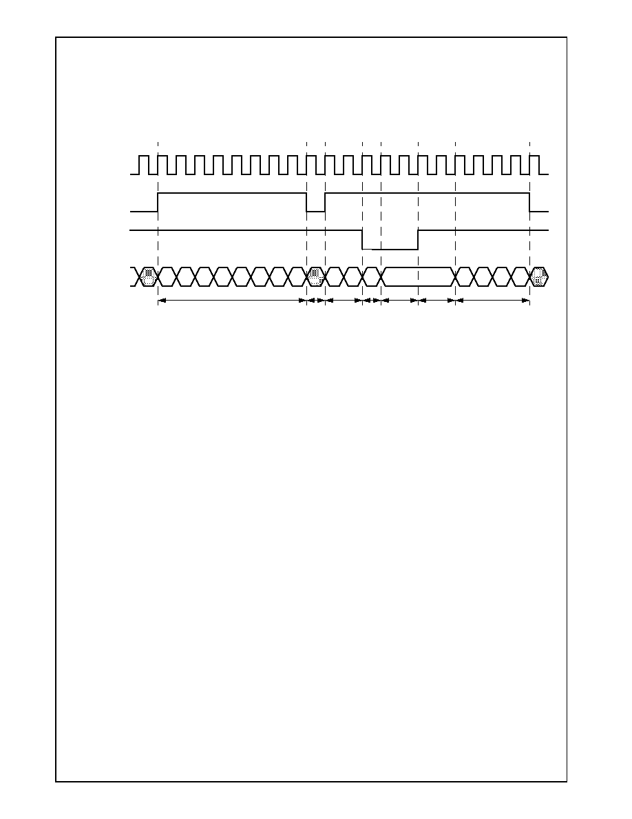
www.national.com
154
Revision 3.1
Integrated Functions (
Continued
)
GeodeTM
G
Xm
Pr
ocessor
4.5.15.1 CS5530 Video Port Data Transfer
VID_VAL indicates that the GXm processor has placed
valid data on VID_DATA[7:0]. VID_RDY indicates that the
CS5530 is ready to accept the next byte of video data.
VID_DATA[7:0] is advanced when both VID_VAL and
VID_RDY are asserted. VID_RDY is driven one clock
early to the GXm processor while VID_VAL is driven coin-
cident with VID_DATA[7:0]. A sample interface functional
timing diagram is shown in Figure 4-17.
Figure 4-17. Video Port Data Transfer (CS5530)
VID_CLK
VID_VAL
8 CLKs
8 + 3 CLKs
VID_RDY
3 CLKs
4 CLKs
VID_DATA
8 CLKs
1
2
CLK
CLKs
1
CLK
2
CLKs
2
CLKs
4 CLKs
Note: VID_CLK = CORE_CLK/2
[7:0]
Revision 3.1
155
www.national.com
Integrated Functions (
Continued
)
GeodeTM
G
Xm
P
r
ocessor
4.6
PCI CONTROLLER
The GXm processor includes an integrated PCI controller
with the following features.
4.6.1
X-Bus PCI Slave
∑ 16-byte PCI write buffer
∑ 16-byte PCI read buffer from X-bus
∑ Supports cache line bursting
∑ Write/Inv line support
∑ Pacing of data for read or write operations with X-bus
∑ No active byte enable transfers supported
4.6.2
X-Bus PCI Master
∑ 16 byte X-bus to PCI write buffer
∑ Configuration read/write Support
∑ Int Acknowledge support
∑ Lock conversion
∑ Support fast back-to-back cycles as slave
4.6.3
PCI Arbiter
∑ Fixed, rotating, hybrid, or ping-pong arbitration
(programmable)
∑ Support four masters, three on PCI
∑ Internal REQ for CPU
∑ Master retry mask counter
∑ Master dead timer
∑ Resource or total system lock support
4.6.4
Generating Configuration Cycles
Configuration space is a physical address space unique to
PCI. Configuration Mechanism #1 must be used by soft-
ware to generate configuration cycles. Two DWORD I/O
locations are used in this mechanism. The first DWORD
location (CF8h) references a read/write register that is
named
CONFIG_ADDRESS.
The
second
DWORD
address
(CFCh)
references
a
register
named
CONFIG_DATA. The general method for accessing con-
figuration
space
is
to
write
a
value
into
CONFIG_ADDRESS that specifies the PCI bus, device on
that bus, and configuration register in that device being
accessed. A read or write to CONFIG_DATA will then
cause the bridge to translate that CONFIG_ADDRESS
value to the requested configuration cycle on the PCI bus.
4.6.5
Generating Special Cycles
A special cycle is a broadcast message to the PCI bus.
Two hardcoded special cycle messages are defined in the
command encode: HALT and SHUTDOWN. Software can
also generate special cycles by using special cycle gener-
ation for configuration mechanism #1 as described in the
PCI Specification 3.6.4.1.2 and briefly described here. To
initiate a special cycle from software, the host must write a
value to CONFIG_ADDRESS encoded as shown in Table
4-36.
The next value written to CONFIG_DATA is the encoded
special cycle. Type 0 or Type 1 conversion will be based
on the Bus Bridge number matching the GXm processor's
bus number of 00h.
Table 4-36. Special-Cycle Code to CONFIG_ADDRESS
31
30
24
23 22 21 20 19 18 17 16 15 14 13 12 11 10
9
8
7
6
5
4
3
2
1
0
1
0 0 0 0 0 0 0
Bus No. = Bridge
1
1
1
1
1
1
1
1
0
0
0
0
0
0
T
T
CONFIG
ENABLE
RSVD
BUS NUMBER
DEVICE NUMBER
FUNCTION
NUMBER
REGISTER NUMBER
TRANS
LATION
TYPE
Note: See Table 4-37 on page 156, bits [1:0] for translation type.
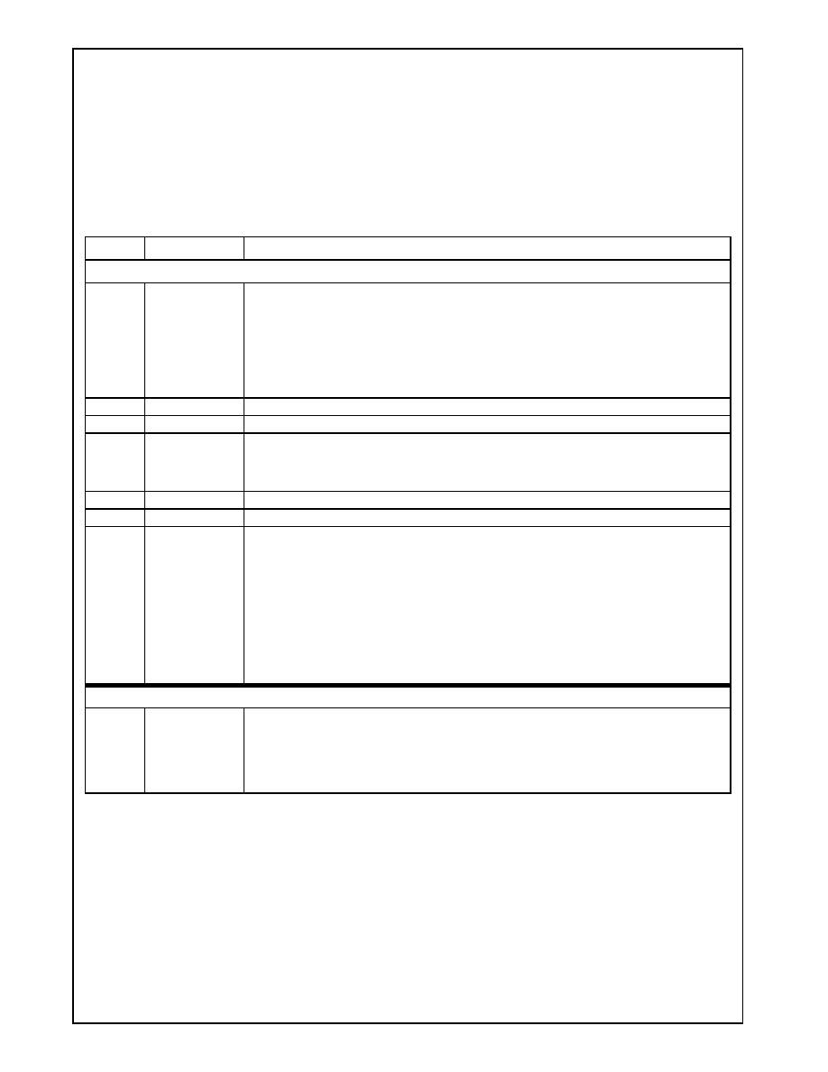
www.national.com
156
Revision 3.1
Integrated Functions (
Continued
)
GeodeTM
G
Xm
Pr
ocessor
4.6.6
PCI Configuration Space Control Registers
There
are
two
registers
in
this
category:
CONFIG_ADDRESS and CONFIG_DATA.
The CONFIG_ADDRESS register contains the address
information for the next configuration space access to
CONFIG_DATA. Only DWORD accesses are permitted to
this register all others will be forwarded as normal I/O
cycles to the PCI bus.
The CONFIG_DATA register contains the data that is sent
or received during a PCI configuration space access.
Table 4-37 gives the bit formats for these two registers.
Table 4-37. PCI Configuration Registers
Bit
Name
Description
I/O Offset 0CF8h-0CFBh
CONFIG_ADDRESS Register (R/W)
Default Value = 00000000h
31
CFG_EN
Config Enable: Determines when accesses should be translated to configuration cycles on the PCI
bus, or treated as a normal I/O operation. This register will be updated only on full DWORD I/O oper-
ations to the CONFIG_ADDRESS. Any other accesses are treated as normal I/O cycles in order to
allow I/O devices to use BYTE or WORD registers at the same address an remain unaffected. Once
bit 31 is set high, subsequent accesses to CONFIG_DATA are then translated to configuration
cycles.
1 = Generate configuration cycles
0 = Normal I/O cycles
30:24
RSVD
Reserved: Set to 0.
23:16
BUS
Bus: Specifies a PCI bus number in the hierarchy of 1 to 256 buses.
15:11
DEVICE
Device: Selects a device on a specified bus. A device value of 00h will select the GXm processor if
the bus number is also 00h. DEVICE values of 01h to 15h will be mapped to AD[31:11], so only 21 of
the 32 possible devices are supported. A DEVICE value of 00001b will map to AD[11] while a device
of 10101b will map to AD[31].
10:8
FUNCTION
Function: Selects a function in a multi-function device.
7:2
REGISTER
Register: Chooses a configuration DWORD space register in the selected device.
1:0
TT
Translation Type Bits: These bits indicate if the configuration access is local or one that requires
translation through other bridges to another PCI bus. When an access occurs to the CONFIG_DATA
address and the specified bus number matches the GXm processor's bus number (00h), then a
Type 0 translation takes place.
For a Type 0 translation, the CONFIG_ADDRESS register values are translated to AD lines on the
PCI bus. Note that bits 10:2 are passed unchanged. The DEVICE value is mapped to one of 21 AD
lines. The translation type bits are set to 00 to indicate a transaction on the local PCI bus.
When an access occurs to the CONFIG_DATA address and the specified bus number is not 00h
(Type 1), the GXm processor passes this cycle to the PCI bus by copying the contents of the
CONFIG_ADDRESS register onto the AD lines during the address phase of the cycle while driving
the translation type bits AD[1:0] to 01.
I/O Offset 0CFCh-0CFFh
CONFIG_DATA (R/W)
Default Value = 00000000h
31:0
CONFIG_DATA
Configuration Data Register: Contains the data that is sent or received during a PCI configuration
space access. The register accessed is determined by the value in the CONFIG_ADDRESS regis-
ter. The CONFIG_DATA register supports BYTE, WORD, or DWORD accesses. To access this reg-
ister, bit 31 of the CONFIG_ADDRESS register must be set to 0 and a full DWORD I/O access must
be done. Configuration cycles are performed when bit 31 of the CONFIG_ADDRESS register is set
to 1
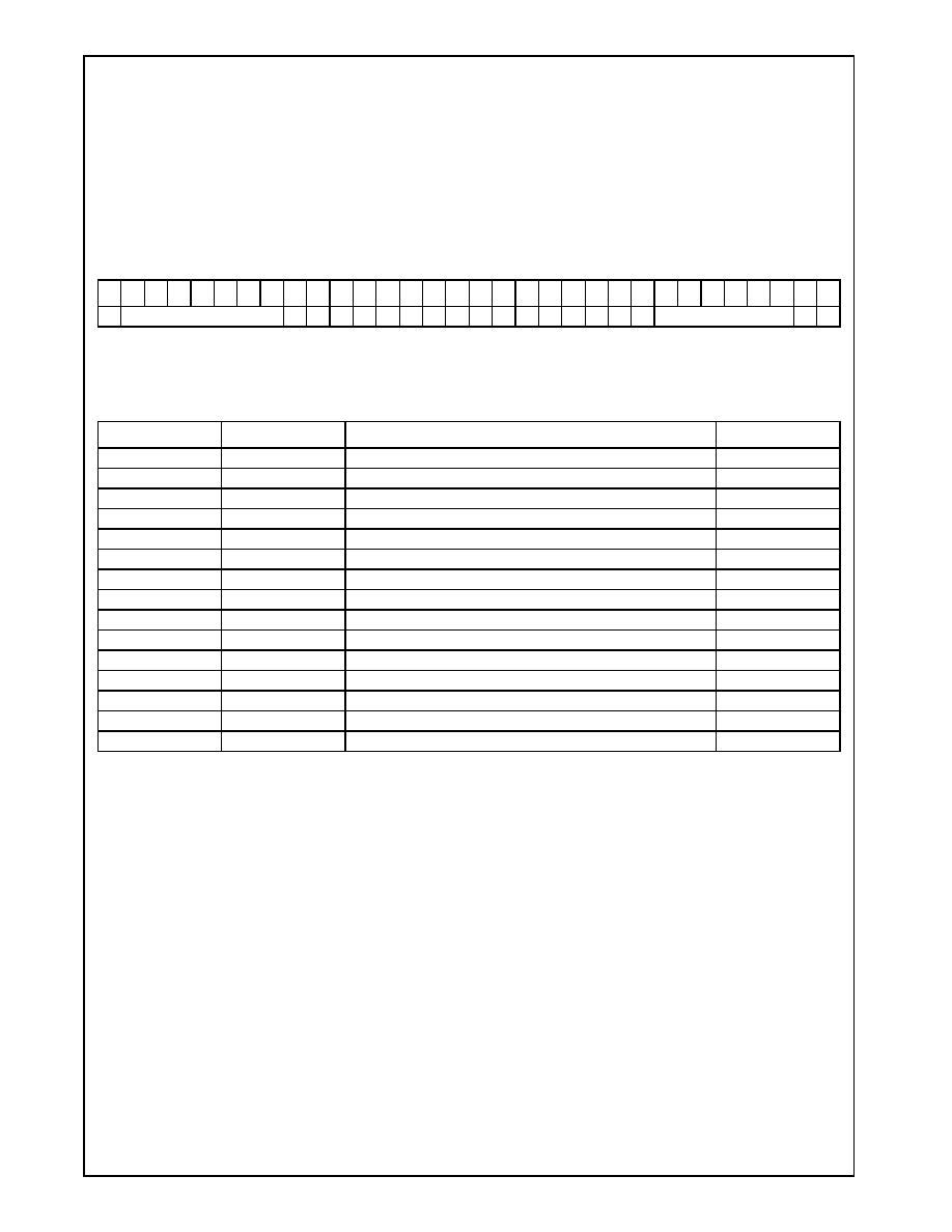
Revision 3.1
157
www.national.com
Integrated Functions (
Continued
)
GeodeTM
G
Xm
P
r
ocessor
4.6.7
PCI Configuration Space Registers
To access the internal PCI configuration registers of the
GXm processor, the Configuration Address Register
(CONFIG_ADDRESS) must be written as a DWORD
using the format shown in Table 4-38. Any other size will
be interpreted as an I/O write to Port 0CF8h. Also, when
entering the Configuration Index, only the six most signifi-
cant bits of the offset are used, and the two least signifi-
cant bits must be 00b.
Table 4-39 summarizes the registers located within the
Configuration Space. The tables that follow, give detailed
register/bit formats.
Table 4-38. Format for Accessing the Internal PCI Configuration Registers
31 30 29 28 27 26 25 24 23 22 21 20 19 18 17 16 15 14 13 12 11 10
9
8
7
6
5
4
3
2
1
0
1
RESERVED
0
0
0
0
0
0
0
0
0
0
0
0
0
0
0
0
Configuration Index
0
0
Table 4-39. PCI Configuration Space Register Summary
Index
Type
Name
Default Value
00h-01h
RO
Vendor Identification
1078h
02h-03h
RO
Device Identification
0001h
04h-05h
R/W
PCI Command
0007h
06h-07h
R/W
Device Status
0280h
08h
RO
Revision Identification
00h
09h-0Bh
RO
Class Code
060000h
0Ch
RO
Cache Line Size
00h
0Dh
R/W
Latency Timer
0Dh
0Eh-3Fh
--
Reserved
00h
40h
R/W
PCI Control Function 1
00h
41h
R/W
PCI Control Function 2
96h
42h
--
Reserved
00h
43h
R/W
PCI Arbitration Control 1
80h
44h
R/W
PCI Arbitration Control 2
00h
45h-FFh
--
Reserved
00h
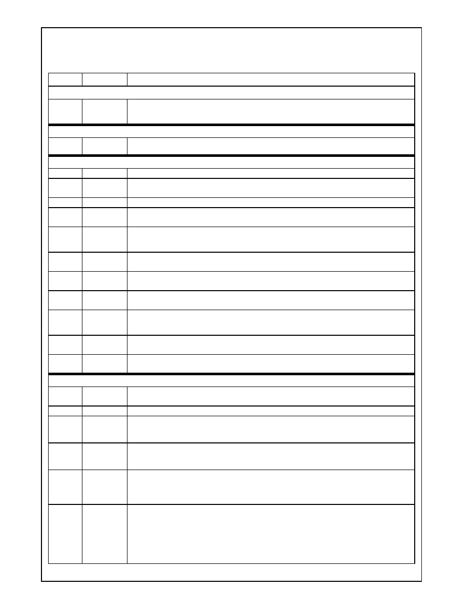
www.national.com
158
Revision 3.1
Integrated Functions (
Continued
)
GeodeTM
G
Xm
Pr
ocessor
Table 4-40. PCI Configuration Registers
Bit
Name
Description
Index 00h-01h
Vendor Identification Register (RO)
Default Value = 1078h
31:0
VID (RO)
Vendor Identification Register (Read Only): The combination of this value and the device ID uniquely
identifies any PCI device. The Vendor ID is the ID given to national Semiconductor Corporation by the
PCI SIG.
Index 02h-03h
Device Identification Register (RO)
Default Value = 0001h
31:0
DIR (RO)
Device Identification Register (Read Only): This value along with the vendor ID uniquely identifies any
PCI device.
Index 04h-05h
PCI Command Register (R/W)
Default Value = 0007h
15:10
RSVD
Reserved: Set to 0.
9
FBE
Fast Back-to-Back Enable: As a master, the GXm processor does not support this function.
This bit returns 0.
8
SERR
SERR# Enable: This is used as an output enable gate for the SERR# driver.
7
WAT
Wait Cycle Control: GXm processor does not do address/ data stepping.
This bit is always set to 0.
6
PE
Parity Error Response:
0 = GXm processor ignores parity errors on the PCI bus.
1 = GXm processor checks for parity errors.
5
VPS
VGA Palette Snoop: GXm processor does not support this function.
This bit is always set to 0.
4
MS
Memory Write and Invalidate Enable: As a master, the GXm processor does not support this function.
This bit is always set to 0.
3
SPC
Special Cycles: GXm processor does not respond to special cycles on the PCI bus.
This bit is always set to 0.
2
BM
Bus Master:
0 = GXm processor does not perform master cycles on the PCI.
1 = GXm processor can act as a bus master on the PCI.
1
MS
Memory Space: GXm processor will always respond to memory cycles on the PCI.
This bit is always set to 1.
0
IOS
I/O Space: GXm processor will not respond to I/O accesses from the PCI.
This bit is always set to 1.
Index 06h-07h
PCI Device Status Register (RO, R/W Clear)
Default Value = 0280h
15
DPE
Detected Parity Error: When a parity error is detected, this bit is set to 1.
This bit can be cleared to 0 by writing a 1 to it.
14
SSE
Signaled System Error: This bit is set whenever SERR# is driven active.
13
RMA
Received Master Abort: This bit is set whenever a master abort cycle occurs. A master abort will occur
whenever a PCI cycle is not claimed except for special cycles.
This bit can be cleared to 0 by writing a 1 to it.
12
RTA
Received Target Abort: This bit is set whenever a target abort is received while the GXm processor is
master of the cycle.
This bit can be cleared to 0 by writing a 1 to it.
11
STA
Signaled Target Abort: This bit is set whenever the GXm processor signals a target abort. A target
abort is signaled when an address parity occurs for an address that hits in the GXm processor's address
space.
This bit can be cleared to 0 by writing a 1 to it.
10:9
DT
Devise Timing:
00 = Fast
01 = Medium
10 = Slow
11 = Reserved
The GXm processor performs medium DEVSEL# active for addresses that hit into the GXm processor
address space. These two bits are always set to 01.

Revision 3.1
159
www.national.com
Integrated Functions (
Continued
)
GeodeTM
G
Xm
P
r
ocessor
8
DPD
Data Parity Detected: This bit is set when three conditions are met.
1) GXm processor asserted PERR# or observed PERR# asserted;
2) GXm processor is the master for the cycle in which the PERR# occurred; and
3) PE (bit 6 of Command Register) is enabled.
This bit can be cleared to 0 by writing a 1 to it.
7
FBS
Fast Back-to-Back Capable: As a target, the processor is capable of accepting Fast Back-to-Back
transactions.
This bit is always set to 1.
6:0
RSVD
Reserved: Set to 0.
Index 08h
Revision Identification Register (RO)
Default Value = 00h
7:0
RID (RO)
Revision ID (Read Only): This register contains the revision number of the GXm design.
Index 09h-0Bh
Class Code Register (RO)
Default Value = 060000h
23:16
CLASS
Class Code: The class code register is used to identify the generic function of the device. The
GXm processor is classified as a host bridge device (06).
15:0
RSVD (RO)
Reserved (Read Only)
Index 0Ch
Cache Line Size Register (RO)
Default Value = 00h
7:0
CACHELINE
Cache Line Size (Read Only): The cache line size register specifies the system cacheline size in units
of 32-bit words. This function is not supported in the GXm processor.
Index 0Dh
Latency Timer Register (R/W)
Default Value = 00h
7:5
RSVD
Reserved: Set to 0.
4:0
LAT_TIMER
Latency Timer: The latency timer as used in this implementation will prevent a system lockup resulting
from a slave the does not responded to the master. If the register value is set to 00h, the timer is dis-
abled. Otherwise, Timer represents the 5 MSBs of an 8-bit counter. The counter will reset on each valid
data transfer. If the counter expires before the next TRDY# is received active, then the slave is consid-
ered to be incapable of responding, and the master will stop the transaction with a master abort and flag
an SERR# active. This would also keep the master from being retried forever by a slave device that con-
tinues to issue retries. In these cases, the master will also stop the cycle with a master abort.
Index 0Eh-3Fh
Reserved
Default Value = 00h
Index 40h
PCI Control Function 1 Register (R/W)
Default Value = 00h
7
RSVD
Reserved: Set to 0.
6
SW
Single Write Mode: PCI slave supports:
0 = Multiple PCI write cycles
1 = Single cycle write transfers on the PCI bus. The slave will perform a target disconnect with the first
data transferred.
5
SR
Single Read Mode: PCI slave supports:
0 = Multiple PCI read cycles.
1 = Single cycle read transfers on the PCI bus. The slave will perform a target disconnect with the first
data transferred.
4
RXBNE
Force Retry when X-Bus Buffers are Not Empty:
0 = PCI slave accepts the PCI cycle with data in the PCI master write buffers. The data in the PCI master
write buffers will not be affected or corrupted. The PCI master holds request active indicating the need to
access the PCI bus.
1 = PCI slave retries cycles if the PCI master X-bus write buffers contain buffered data.
3
SWBE
PCI Slave Write Buffer Enable: PCI slave write buffers: 0 = Disable; 1 = Enable.
2
CLRE
PCI Cache Line Read Enable: Read operations from the PCI into the GXm processor:
0 = Single cycle unless a read multiple or memory read line command is used.
1 = Cause a cache line read to occur.
1
XBE
X-Bus Burst Enable: PCI slave acting as a master performs burst cycles on the X-bus on write-back
invalidate cycles from the PCI. 0 = Disable; 1 = Enable.
(This bit does not control read bursting; bit 2 does.)
0
RSVD
Reserved: Should return a value of 0.
Table 4-40. PCI Configuration Registers (Continued)
Bit
Name
Description

www.national.com
160
Revision 3.1
Integrated Functions (
Continued
)
GeodeTM
G
Xm
Pr
ocessor
Index 41h
PCI Control Function 2 Register (R/W)
Default Value = 96h
7
RSVD
Reserved: Set to 0.
6
RW_CLK
RAW Clock: A debug signal used to view internal clock operation. 0 = Disable; 1 = Enable.
5
PFS
PERR# forces SERR#: PCI master drives an active SERR# anytime it also drives or receives an active
PERR#: 0 = Disable; 1 = Enable.
4
XWB
X-Bus to PCI Write Buffer: Enable GXm processor PCI master's X-Bus write buffers (non-locked mem-
ory cycles are buffered, I/O cycles and lock cycles are not buffered): 0 = Disable; 1 = Enable.
3:2
SDB
Slave Disconnect Boundary: PCI slave issues a disconnect with data when it crosses line boundary:
00 = 128 bytes
01 = 256 bytes
10 = 512 bytes
11 = 1024 bytes
Works in conjunction with bit 1.
1
SDBE
Slave Disconnect Boundary Enable:
0 = PCI slave disconnects on boundaries set by bits [3:2].
1 = PCI disconnects on cache line boundary which is 16 bytes.
0
XWS
X-Bus Wait State Enable: The PCI slave acting as a master on the X-bus will insert wait states on write
cycles for data setup time. 0 = Disable; 1 = Enable.
Index 43h
PCI Arbitration Control 1 Register (R/W)
Default Value = 80h
7
BG
Bus Grant:
0 = Grants bus regardless of X-bus buffers.
1 = Grants bus only if X-bus buffers are empty.
6
RSVD
Reserved: Set to 1.
5
RME2
REQ2# Retry Mask Enable: Arbiter allows the REQ2# to be masked based on the master retry mask in
bits [2:1]: 0 = Disable; 1 = Enable.
4
RME1
REQ1# Retry Mask Enable: Arbiter allows the REQ1# to be masked based on the master retry mask in
bits [2:1]: 0 = Disable; 1 = Enable.
3
RME0
REQ0# Retry Mask Enable: Arbiter allows the REQ0# to be masked based on the master retry mask in
bits [2:1]: 0 = Disable; 1 = Enable.
2:1
MRM
Master Retry Mask: When a target issues a retry to a master, the arbiter can mask the request from the
retried master in order to allow other lower order masters to gain access to the PCI bus:
00 = No retry mask
01 = Mask for 16 PCI clocks
10 = Mask for 32 PCI clocks
11 = Mask for 64 PCI clocks
0
HXR
Hold X-bus on Retries: Arbiter holds the X-Bus X_HOLD for two additional clocks to see if the retried
master will request the bus again: 0 = Disable; 1 = Enable
(This may prevent retry thrashing in some cases.)
Table 4-40. PCI Configuration Registers (Continued)
Bit
Name
Description
Revision 3.1
161
www.national.com
Integrated Functions (
Continued
)
GeodeTM
G
Xm
P
r
ocessor
Index 44h
PCI Arbitration Control 2 Register (R/W)
Default Value = 00h
7
PP
Ping-Pong:
0 = Arbiter grants the processor bus per the setting of bits [2:0].
1 = Arbiter grants the processor bus ownership of the PCI bus every other arbitration cycle.
6:4
FAC
Fixed Arbitration Controls: These bits control the priority under fixed arbitration. The priority table is as
follows (priority listed highest to lowest):
000 = REQ0#, REQ1#, REQ2#
001 = REQ1#, REQ0#, REQ2#
010 = REQ0#, REQ2#,REQ1#
011 = Reserved
100 = REQ1#, REQ2#, REQ0#
101 = Reserved
110 = REQ2#, REQ1#, REQ0#
111 = REQ2#, REQ0#, REQ1#
Note: The rotation arbitration bits [2:0] must be set to 000 for full fixed arbitration. If rotation bits are not
set to 000, then hybrid arbitration will occur. If Ping-Pong is enabled (bit 7 = 1), the processor will
have priority every other arbitration. In this mode, the arbiter grants the PCI bus to a master and
ignores all other requests. When the master finishes, the processor will be guaranteed access. At
this point PCI requests will again be recognized. This will switch arbitration from CPU-to-PCI to
CPU-to-PCI, etc.
3
RSVD
Reserved: Set to 0.
45h-FFh
--
Reserved
Table 4-40. PCI Configuration Registers (Continued)
Bit
Name
Description
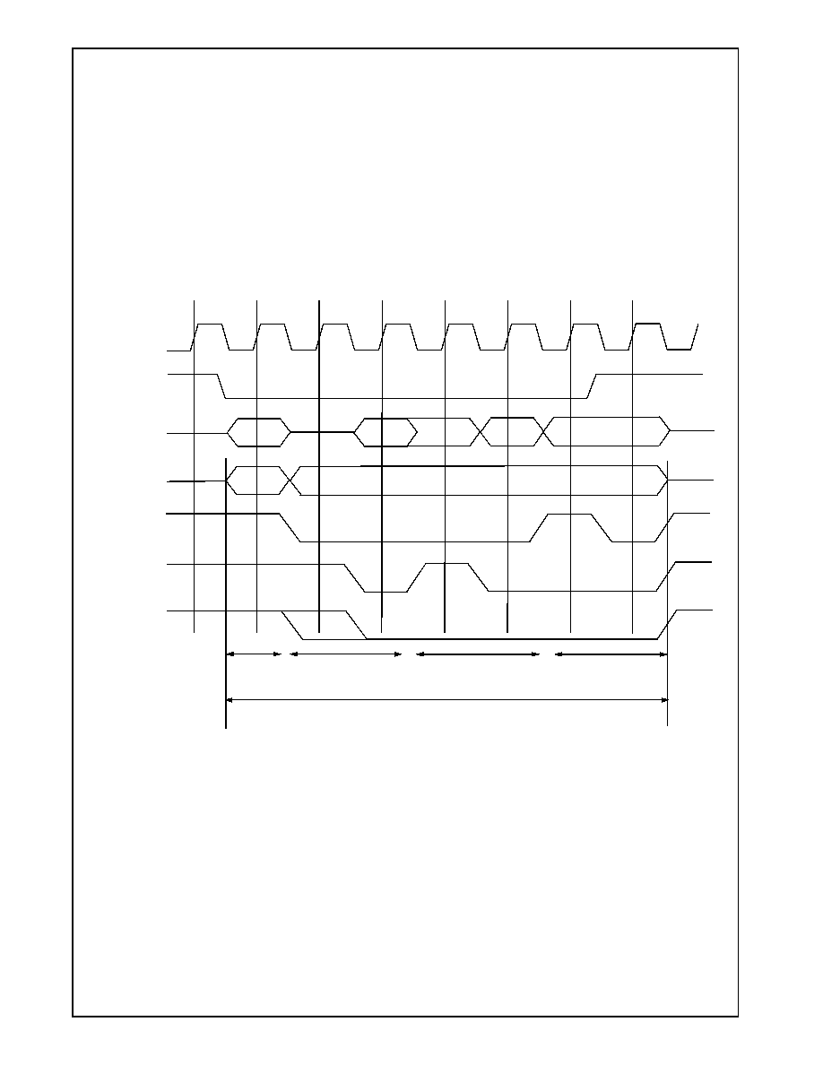
www.national.com
162
Revision 3.1
Integrated Functions (
Continued
)
GeodeTM
G
Xm
Pr
ocessor
4.6.8
PCI Cycles
The following sections and diagrams provide the func-
tional relationships for PCI cycles.
4.6.8.1
PCI Read Transaction
A PCI read transaction consists of an address phase and
one or more data phases. Data phases may consist of
wait cycles and a data transfer. Figure 4-18 illustrates a
PCI read transaction. In this example, there are three data
phases.
The address phase begins on clock 2 when FRAME# is
asserted. During the address phase, AD[31:0] contains a
valid address and C/BE[3:0]# contains a valid bus com-
mand. The first data phase begins on clock 3. During the
data phase, AD[31:0] contains data and C/BE[3:0]# indi-
cate which byte lanes of AD[31:0] carry valid data. The
first data phase completes with zero delay cycles. How-
ever, the second phase is delayed one cycle because the
target was not ready so it deasserted TRDY# on clock 5.
The last data phase is delayed one cycle because the
master deasserted IRDY# on clock 7.
For additional information refer to Chapter 3.3.1, Read
Transaction, of the PCI Local Bus Specification, Revision
2.1.
Figure 4-18. Basic Read Operation
CLK
FRAME#
AD
C/BE#
DATA-1
DATA-2
DATA-3
ADDR
BUS CMD
BE#s
IRDY#
TRDY#
DEVSEL#
BUS TRANSACTION
ADDR
PHASE
DATA
PHASE
DATA
PHASE
DATA
PHASE
D
A
T
A
T
R
A
N
SF
ER
WA
I
T
WA
I
T
D
A
T
A
T
R
A
N
SF
ER
WA
I
T
D
A
T
A
T
R
AN
S
F
ER
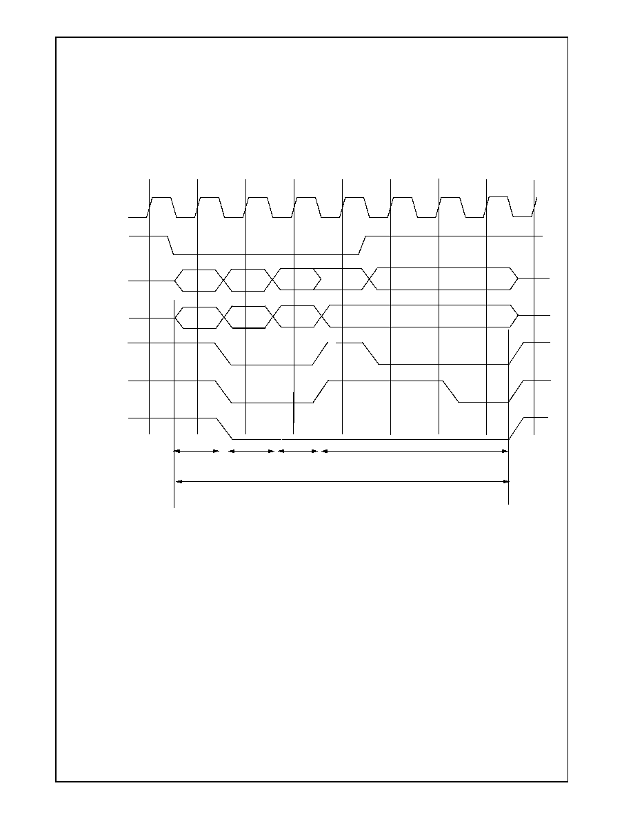
Revision 3.1
163
www.national.com
Integrated Functions (
Continued
)
GeodeTM
G
Xm
P
r
ocessor
4.6.8.2
PCI Write Transaction
A PCI write transaction is similar to a PCI read transac-
tion, consisting of an address phase and one or more data
phases. Since the master provides both address and
data, no turnaround cycle is required following the
address phase. The data phases work the same for both
read and write transactions. Figure 4-19 illustrates a write
transaction.
The address phase begins on clock 2 when FRAME# is
asserted. The first and second data phases complete
without delays. During data phase 3, the target inserts
three wait cycles by deasserting TRDY#.
For additional information refer to Chapter 3.3.2, Write
Transaction, of the PCI Local Bus Specification, Revision
2.1.
Figure 4-19. Basic Write Operation
CLK
FRAME#
AD
C/BE#
DATA-2
DATA-3
ADDR
IRDY#
TRDY#
DEVSEL#
BUS TRANSACTION
ADDR
PHASE
DATA
PHASE
DATA
PHASE
DATA
PHASE
D
A
TA
T
R
A
N
SF
ER
WAI
T
WAI
T
WA
IT
D
A
TA
T
R
AN
S
F
ER
DATA-1
BE#'s-2
BE#'s-3
BUS CMD
BE#'s-1
D
A
T
A
T
R
AN
SF
ER

www.national.com
164
Revision 3.1
Integrated Functions (
Continued
)
GeodeTM
G
Xm
Pr
ocessor
4.6.8.3
PCI Arbitration
An agent requests the bus by asserting its REQ#. Based
on the arbitration scheme set in the PCI Arbitration Con-
trol 2 Register (Index 44h), the GX PCI arbiter will grant
the request by asserting GNT#. Figure 4-20 illustrates
basic arbitration.
REQ#-a is asserted at clock 1. The PCI GXm processor
arbiter grants access to Agent A by asserting GNT#-a on
clock 2. Agent A must begin a transaction by asserting
FRAME# within 16 clocks, or the GX PCI arbiter will
remove GNT#. Also, it is possible for Agent A to lose bus
ownership sooner if another agent with higher priority
requests the bus. However, in this example, Agent A
starts the transaction on clock 3 by asserting FRAME#
and completes its transaction. Since Agent A requests
another transaction, REQ#-a remains asserted. When
FRAME# is asserted on clock 3, the GXm processor's PCI
arbiter determines Agent B should go next, asserts
GNT#-b and deasserts GNT#-a on clock 4. Agent B
requires only a single transaction. It completes the trans-
action, then deasserts FRAME# and REQ#-b on clock 6.
The GXm processor's PCI arbiter can then grant access
to agent A, and does so on clock 7. Note that all buffers
must flush before a grant is given to a new agent.
For additional information refer to Chapter 3.4.1, Arbitra-
tion Signaling Protocol, of the PCI Local Bus Specifica-
tion, Revision 2.1.
4.6.8.4
PCI Halt Command
Halt is a broadcast message from the processor indicating
it has executed a halt instruction. The PCI Special Cycle
command is used to broadcast the message to all agents
on the bus segment. During the address phase of the Halt
Special cycle, C/BE[3:0]# = 0001 and AD[31:0] are driven
to random values. During the data phase, C/BE[3:0]# =
1100 indicating bytes 1 and 0 are valid and AD[15:0] =
0001h.
For additional information, refer to Chapter 3.7.2, Special
Cycle, and Appendix A, Special Cycle Messages, of the
PCI Local Bus Specification, Revision 2.1.
Figure 4-20. Basic Arbitration
CLK
REQ#-a
REQ#-b
GNT#-a
GNT#-b
FRAME#
AD
DATA
ADDR
DATA
ADDR
access-a
access-b

Revision 3.1
165
www.national.com
GeodeTM
G
Xm
P
r
ocessor
5.0
Virtual Subsystem Architecture
This section describes the Virtual Subsystem Architec-
ture
Æ
(VSATM) as implemented with the Geode GXm pro-
cessor(s) and VSA enhanced I/O companion device(s).
VSA provides a framework to enable software implemen-
tation of traditionally hardware-only components. VSA
software executes in System Management Mode (SMM),
enabling it to execute transparently to the operating sys-
tem, drivers and applications.
The VSA design is based upon a simple model for replac-
ing hardware components with software. Hardware to be
virtualized is merely replaced with simple access detec-
tion circuitry which asserts the processor's SMI# (System
Management Interrupt) pin when hardware accesses are
detected. The current execution stream is immediately
preempted, and the processor enters SMM. The SMM
system software then saves the processor state, initializes
the VSA execution environment, decodes the SMI source
and dispatches handler routines which have registered
requests to service the decoded SMI source. Once all
handler routines have completed, the processor state is
restored and normal execution resumes. In this manner,
hardware accesses are transparently replaced with the
execution of SMM handler software.
Historically, SMM software was used primarily for the sin-
gle purpose of facilitating active power management for
notebook designs. That software's only function was to
manage the power up and down of devices to save power.
With high performance processors now available, it is fea-
sible to implement, primarily in SMM software, PC capa-
bilities traditionally provided by hardware. In contrast to
power management code, this virtualization software gen-
erally has strict performance requirements to prevent
application
performance
from
being
significantly
impacted.
Several functions can be virtualized in a GXm processor
based design using the VSA environment. The VSA
enhanced chipsets provide programmable resources to
trap both memory and I/O accesses. However, specific
hardware is included to support the virtualization of VGA
core compatibility and audio functionality in the system.
The hardware support for VGA emulation resides com-
pletely inside the GXm processor. Legacy VGA accesses
do not generate off-chip bus cycles. However, the VSA
support hardware for
XpressAUDIO resides in the CS5530 I/O companion
device and is described in the CS5530 specification.
5.1
VIRTUAL VGA
The GXm processor reduces the burden of PC-legacy
hardware by using a balanced mix of hardware and soft-
ware to provide the same functionality. The graphics pipe-
line contains full hardware support for the VGA "front-
end", the logic that controls read and write operations to
the VGA frame buffer (located in graphics memory). For
some modes, the hardware can also provide direct display
of the data in the VGA buffer. Virtual VGA traps frame
buffer accesses only when necessary, but it must trap all
VGA I/O accesses to maintain the VGA state and properly
program the graphics pipeline and display controller.
VGA functionality with the GXm processor includes the
standard VGA modes (VGA, EGA, CGA, and MDA) as
well as the higher-resolution VESA modes. The CGA and
MDA modes (modes 0 through 7) require that Virtual VGA
convert the data in the VGA buffer to a separate 8-BPP
frame buffer that the hardware can use for display refresh.
The remaining modes, VGA, EGA, and VESA, can be dis-
played directly by the hardware, with no data conversion
required. For these modes, Virtual VGA outperforms typi-
cal VGA cards because the frame buffer data does not
travel across an external bus.
Display drivers for popular GUI (graphical user interface)
based operating systems are provided by National Semi-
conductor which enable a full featured 2D hardware accel-
erator to be used instead of the emulated VGA core.
5.1.1
Traditional VGA Hardware
A VGA card consists of display memory and control regis-
ters. The VGA display memory shows up in system mem-
ory between addresses A0000h and BFFFFh. It is
possible to map this memory to three different ranges
within this 128 KB block.
The first range is
- A0000h to B0000h for EGA and VGA modes,
the second range is
- B0000h to B7FFFh for MDA modes,
and the third range is
- B8000h to BFFFFh for CGA modes.
The VGA control registers are mapped to the I/O address
range from 3B0h to 3DFh. The VGA registers are
accessed with an indexing scheme that provides more
registers than would normally fit into this range. Some
registers are mapped at two locations, one for mono-
chrome, and another for color.
The VGA hardware can be accessed by calling BIOS rou-
tines or by directly writing to VGA memory and control
registers. DOS always calls BIOS to set up the display
mode and render characters. Many other applications
access the VGA memory and control registers directly.
The VGA card can be set up to a virtually unlimited num-
ber of modes. However, many applications use one of the
predefined modes specified by the BIOS routine which
sets up the display mode. The predefined modes are
translated into specific VGA control register setups by the
BIOS. The standard modes supported by VGA cards are
shown in Table 5-1.

www.national.com
166
Revision 3.1
Virtual Subsystem Architecture (
Continued
)
GeodeTM
G
Xm
Pr
ocessor
A VGA is made up of several functional units.
∑ The frame buffer is 256 KB of memory that provides
data for the video display. It is organized as 64 K 32-bit
DWORDs.
∑ The sequencer decomposes word and DWORD CPU
accesses into byte operations for the graphics
controller. It also controls a number of miscellaneous
functions, including reset and some clocking controls.
∑ The graphics controller provides most of the interface
between CPU data and the frame buffer. It allows the
programmer to read and write frame buffer data in
different formats. Plus provides ROP (raster operation)
and masking functions.
∑ The CRT controller provides video timing signals and
address generation for video refresh. It also provides a
text cursor.
∑ The attribute controller contains the video refresh
datapath, including text rasterization and palette
lookup.
∑ The general registers provide status information for
the programmer as well as control over VGA-host
address mapping and clock selection. This is all
handled in hardware by the graphics pipeline.
It is important to understand that a VGA is constructed of
numerous independent functions. Most of the register
fields correspond to controls that were originally built out
of discrete logic or were part of a dedicated controller
such as the 6845. The notion of a VGA "mode" is a higher-
level convention to denote a particular set of values for the
registers. Many popular programs do not use standard
modes, preferring instead to produce their own VGA set-
ups that are optimal for their purposes.
5.1.1.1
VGA Memory Organization
The VGA memory is organized as 64 K 32-bit DWORDs.
This organization is usually presented as four 64 KB
"planes". A plane consists of one byte out of every
DWORD. Thus, plane 0 refers to the least significant byte
from every one of the 64 K DWORDs. The addressing
granularity of this memory is a DWORD, not a byte; that is,
consecutive addresses refer to consecutive DWORDs.
The only provision for byte-granularity addressing is the
four-byte enable signals used for writes. In C parlance,
single_plane_byte = (dword_fb[address] >>
(plane * 8)) & 0xFF;
When dealing with VGA, it is important to recognize the
distinction
between
host
addresses,
frame
buffer
addresses, and the refresh address pipe. A VGA control-
ler contains lots of hardware to translate between these
address spaces in different ways, and understanding
these translations is critical to understanding the entire
device. In standard four-plane graphics modes, a frame-
buffer DWORD provides eight 4-bit pixels. The left-most
pixel comes from bit 7 of each plane, with plane 3 provid-
ing the most significant bit.
pixel[i].bit[j] = dword_fb[address].bit[j*8 + (7-i)]
5.1.1.2
VGA Front End
The VGA front end consists of address and data transla-
tions between the CPU and the frame buffer. This func-
tionality is contained within the graphics controller and
sequencer components. Most of the front end functionality
is implemented in the VGA read and write hardware of the
GXm processor. An important axiom of the VGA is that
the front end and back end are controlled independently.
There are no register fields that control the behavior of
both pieces. Terms like "VGA odd/even mode" are there-
fore somewhat misleading; there are two different controls
for odd/even functionality in the front end, and two sepa-
rate controls in the refresh path to cause "sensible"
refresh behavior for frame buffer contents written in
odd/even mode. Normally, all these fields would be set up
together, but they don't have to be. This sort of orthogonal
behavior gives rise to the enormous number of possible
VGA "modes". The CPU end of the read and write pipes is
one byte wide. Word and DWORD accesses from the
Table 5-1. Standard VGA Modes
Category
Mode
Text or
Graphics
Resolution
Format
Type
Software
0,1
Text
40x25
Characters
CGA
2,3
Text
80x25
Characters
CGA
4,5
Graphics
320x200
2 BPP
CGA
6
Graphics
640x200
1 BPP
CGA
7
Text
80x25
Characters
MDA
Hardware
0Dh
Graphics
320x200
4 BPP
EGA
0Eh
Graphics
640x200
4 BPP
EGA
0Fh
Graphics
640x350
1 BPP
EGA
10h
Graphics
640x350
4 BPP
EGA
11h
Graphics
640x480
1 BPP
VGA
12h
Graphics
640x480
4 BPP
VGA
13h
Graphics
320x200
8 BPP
VGA

Revision 3.1
167
www.national.com
Virtual Subsystem Architecture (
Continued
)
GeodeTM
G
Xm
P
r
ocessor
CPU to VGA memory are broken down into multiple byte
accesses by the sequencer. For example, a word write to
A0000h (in a VGA graphics mode) is processed as if it
were two-byte write operations to A0000h and A0001h.
5.1.1.3
Address Mapping
When a VGA card sees an address on the host bus, bits
[31:15] determine whether the transaction is for the VGA.
Depending
on
the
mode,
addresses
000AXXXX,
000B{0XXX}XXX, or 000B{1XXX}XXXX can decode into
VGA space. If the access is for the VGA, bits [15:0] pro-
vide the DWORD address into the frame buffer (however,
see odd/even and Chain 4 modes, below). Thus, each
byte address on the host bus addresses a DWORD in
VGA memory.
On a write transaction, the byte enables are normally
driven from the sequencer's MapMask register. The VGA
has two other write address mappings that modify this
behavior. In odd/even (Chain 2) write mode, bit 0 of the
address is used to enable bytes 0 and 2 (if zero) or bytes
1 and 3 (if one). In addition, the address presented to the
frame buffer has bit 0 replaced with the PageBit field of
the Miscellaneous Output register. Chain 4 write mode is
similar; only one of the four byte enables is asserted,
based on bits [1:0] of the address, and bits [1:0] of the
frame buffer address are set to zero. In each of these
modes, the MapMask enables are logically ANDed into
the enables that result from the address.
5.2
GXM VIRTUAL VGA
The GXm processor provides VGA compatibility through a
mixture of hardware and software. The processor core
contains SMI generation hardware for VGA memory write
operations. The bus controller contains SMI generation
hardware for VGA I/O read and write operations. The
graphics pipeline contains hardware to detect and pro-
cess reads and writes to VGA memory. VGA memory is
partitioned from system memory.
5.2.1
Datapath Elements
The graphics controller contains several elements that
convert between host data and frame buffer data.
The rotator simply rotates the byte written from the host
by 0 to 7 bits to the right, based on the RotateCount field
of the DataRotate register. It has no effect in the read
path.
The display latch is a 32-bit register that is loaded on
every read access to the frame buffer. All 32 bits of the
frame buffer DWORDs are loaded into the latch.
The write-mode unit converts a byte from the host into a
32-bit value. A VGA has four write modes:
∑ Write Mode 0:
- Bit n of byte b comes from one of two places,
depending on bit b of the EnableSetReset register. If
that bit is zero, it comes from bit n of the host data. If
that bit is one, it comes from bit b of the SetReset
register. This mode allows the programmer to set
some planes from the host data and the others from
SetReset.
∑ Write Mode 1:
- All 32 bits come directly out of the display latch; the
host data is ignored. This mode is used for screen-
to-screen copies.
∑ Write Mode 2:
- Bit n of byte b comes from bit b of the host data; that
is, the four LSBs of the host data are each replicated
through a byte of the result. In conjunction with the
BitMask register, this mode allows the programmer
to directly write a 4-bit color to one or more pixels.
∑ Write Mode 3:
- Bit n of byte b comes from bit b of the SetReset
register. The host data is ANDed with the BitMask
register to provide the bit mask for the write (see
below).
The read mode unit converts a 32-bit value from the
frame buffer into a byte. A VGA has two read modes:
∑ Read Mode 0:
- One of the four bytes from the frame buffer is
returned, based on the value of the ReadMapSelect
register. In Chain 4 mode, bits [1:0] of the read
address select a plane. In odd/even read mode, bit 0
of the read address replaces bit 0 of ReadMapSe-
lect.
∑ Read Mode 1:
- Bit n of the result is set to 1 if bit n in every byte b
matches bit b of the ColorCompare register; other-
wise it is set to 0. There is a ColorDon'tCare register
that can exclude planes from this comparison. In
four-plane graphics modes, this provides a conver-
sion from 4 BPP to 1 BPP.
The ALU is a simple two-operand ROP unit that operates
on writes. Its operating modes are COPY, AND, OR, and
XOR. The 32-bit inputs are:
1) the output of the write-mode unit and
2) the display latch (not necessarily the value at the
frame buffer address of the write).
An application that wishes to performs ROPs on the
source and destination must first byte read the address (to
load the latch) and then immediately write a byte to the
same address. The ALU has no effect in Write Mode 1.
The bit mask unit does not provide a true bit mask.
Instead, it selects between the ALU output and the display
latch. The mask is an 8-bit value, and bit n of the mask
makes the selection for bit n of all four bytes of the result
(a zero selects the latch). No bit masking occurs in Write
Mode 1.
The VGA hardware of the GXm processor does not imple-
ment Write Mode 1 directly, but it can be indirectly imple-
mented by setting the BitMask to zero and the ALU mode
to COPY.

www.national.com
168
Revision 3.1
Virtual Subsystem Architecture (
Continued
)
GeodeTM
G
Xm
Pr
ocessor
5.2.2
Video Refresh
VGA refresh is controlled by two units: the CRT controller
(CRTC) and the attribute controller (ATTR). The CRTC
provides refresh addresses and video control; the ATTR
provides the refresh datapath, including pixel formatting
and internal palette lookup.
The VGA back end contains two basic clocks: the dot
clock (or pixel clock) and the character clock. The Clock-
Select field of the Miscellaneous Output register selects a
"master clock" of either 25 MHz or 28 MHz. This master
clock, optionally divided by two, drives the dot clock. The
character clock is simply the dot clock divided by eight or
nine.
The VGA supports four basic pixel formats. Using text for-
mat, the VGA interprets frame buffer values as ASCII
characters, foreground/background attributes, and font
data. The other three formats are all "graphics modes",
known as APA (All Points Addressable) modes. These for-
mats could be called CGA-compatible (odd/even four
bits/pixel), EGA-compatible (4-plane four bits/pixel), and
VGA-compatible (pixel-per-byte eight bits/pixel). The for-
mat is chosen by the ShiftRegister field of the Graphics
Controller Mode register.
The refresh address pipe is an integral part of the CRTC,
and has many configuration options. Refresh can begin at
any frame buffer address. The display width and the frame
buffer pitch (scan-line delta) are set separately. Multiple
scan lines can be refreshed from the same frame buffer
addresses. The LineCompare register causes the refresh
address to be reset to zero at a particular scan line, pro-
viding support for vertical split-screen.
Within the context of a single scan line, the refresh
address increments by one on every character clock.
Before being presented to the frame buffer, refresh
addresses can be shifted by 0, 1, or 2 bits to the left.
These options are often mis-named Byte, Word, and Dou-
bleword modes. Using this shifter, the refresh unit can be
programmed to skip one out of two or three out of four
DWORDs of refresh data. As an example of the utility of
this function, consider Chain 4 mode, described earlier.
Pixels written in Chain 4 mode occupy one out of every
four DWORDs in the frame buffer. If the refresh path is put
into "Doubleword" mode, the refresh will come only from
those DWORDs writable in Chain 4. This is how VGA
mode 13h works.
In text mode, the ATTR has a lot of work to do. At each
character clock, it pulls a DWORD of data out of the frame
buffer. In that DWORD, plane 0 contains the ASCII char-
acter code, and plane 1 contains an attribute byte. The
ATTR uses plane 0 to generate a font lookup address and
read another DWORD. In plane 2, this DWORD contains a
bit-per-pixel representation of one scan line in the appro-
priate character glyph. The ATTR transforms these bits
into eight pixels, obtaining foreground and background
colors from the attribute byte. The CRTC must refresh
from the same memory addresses for all scan lines that
make up a character row; within that row, the ATTR must
fetch successive scan lines from the glyph table so as to
draw proper characters. Graphics modes are somewhat
simpler. In CGA-compatible mode, a DWORD provides
eight pixels. The first four pixels come from planes 0 and
2; each 4-bit pixel gets bits [3:2] from plane 2, and bits
[1:0] from plane 0. The remaining four pixels come from
planes 1 and 3. The EGA-compatible mode also gets
eight pixels from a DWORD, but each pixel gets one bit
from each plane, with plane 3 providing bit 3. Finally,
VGA-compatible mode gets four pixels
from
each
DWORD; plane 0 provides the first pixel, plane 1 the next,
and so on. The 8 BPP mode uses an option to provide
every pixel for two dot clocks, thus allowing the refresh
pipe to keep up (it only increments on character clocks)
and meaning that the 320-pixel-wide mode 13h really has
640 visible pixels per line. The VGA color model is
unusual. The ATTR contains a 16-entry color palette with
6 bits per entry. Except for 8 BPP modes, all VGA configu-
rations drive four bits of pixel data into the palette, which
produces a 6-bit result. Based on various control regis-
ters, this value is then combined with other register con-
tents to produce an 8-bit index into the DAC. There is a
ColorPlaneEnable register to mask bits out of the pixel
data before it goes to the palette; this is used to emulate
four-color CGA modes by ignoring the top two bits of each
pixel. In 8 BPP modes, the palette is bypassed and the
pixel data goes directly to the DAC
5.2.3
GXm VGA Hardware
The GXm processor core contains hardware to detect
VGA accesses and generate SMI interrupts. The graphics
pipeline contains hardware to detect and process reads
and writes to VGA memory. The VGA memory on the
GXm processor is partitioned from system memory. The
GXm processor has the following hardware components
to assist the VGA emulation software.
∑
SMI Generation
∑
VGA Range Detection
∑
VGA Sequencer
∑
VGA Write/Read Path
∑
VGA Address Generator
∑
VGA Memory
5.2.3.1
SMI Generation
VGA emulation software is notified of VGA memory
accesses by an SMI generated in dedicated circuitry in
the processor core that detects and traps memory
accesses. The SMI generation hardware for VGA memory
addresses is in the second stage of instruction decoding
on the processor core. This is the earliest stage of instruc-
tion decode where virtual addresses have been translated
to physical addresses. Trapping after the execution stage
is impractical, because memory write buffering will allow
subsequent instructions to execute.
The VGA emulation code requires the SMI to be gener-
ated immediately when a VGA access occurs. The SMI
generation hardware can optionally exclude areas of VGA
memory, based on a 32-bit register which has a control bit
for each 2 KB region of the VGA memory window. The

Revision 3.1
169
www.national.com
Virtual Subsystem Architecture (
Continued
)
GeodeTM
G
Xm
P
r
ocessor
control bit determines whether or not an SMI interrupt is
generated for the corresponding region. The purpose of
this hardware is to allow the VGA emulation software to
disable SMI interrupts in VGA memory regions that are
not currently displayed.
For direct display modes (8 BPP or 16 BPP) in the display
controller, Virtual VGA can operate without SMI genera-
tion.
The SMI generation circuit on the GXm processor has
configuration registers to control and mask SMI interrupts
in the VGA memory space.
5.2.3.2
VGA Memory Addresses
SMI generation can be configured to trap VGA memory
accesses in one of the following ranges:
A0000h to AFFFFh (EGA,VGA),
B0000h to B7FFFh (MDA),
or B8000h to BFFFFh (CGA).
Range selection is accomplished through programmable
bits in the VGACTL register (Index B9h). Fine control can
be exercised within the range selected to allow off-screen
accesses to occur without generating SMIs.
SMI generation can also separately control the following
I/O ranges: 3B0h to 3BFh, 3C0h to 3CFh, and 3D0h to
3DFh. The BC_XMAP_1 register (GX_BASE+8004h) in
the Internal Bus Interface Unit has an enable/disable bit
for each of the address ranges above.
5.2.3.3
VGA Configuration Registers
Table 5-2 summarizes the VGA Configuration Registers.
Detailed register/bit formats are given in Table 5-3.
5.2.3.4
VGA Control Register
The VGA control register (VGACTL) provides control for
SMI generation through an enable bit for memory address
ranges A0000h to BFFFFh. Each bit controls whether or
not SMI is generated for accesses to the corresponding
address range. The default value of this register is zero so
that VGA accesses will not be trapped on systems with an
external VGA card.
5.2.3.5
VGA Mask Registers
The VGA Mask register (VGAM) has 32 bits that can
selectively mask 2 KB regions within the VGA memory
region A0000h to AFFFFh. If none of the three regions is
enabled in VGACTL, then the contents of VGAM are
ignored. VGAM can be used to prevent the occurrence of
SMI when non-displayed VGA memory is accessed. This
is an enhancement that improves performance for double-
buffered applications only.
Table 5-2. VGA Configuration Registers Summary
Index
Name
Description
Default
B9h
VGACTL
VGA Control Register
00h (SMI generation disabled)
BAh-BDh
VGAM
VGA Mask Register
Don't Care

www.national.com
170
Revision 3.1
Virtual Subsystem Architecture (
Continued
)
GeodeTM
G
Xm
Pr
ocessor
Table 5-3. VGA Configuration Registers
Bit
Description
Index B9h
VGACTL Register (R/W)
Default Value = 00h
7:3
Reserved: Set to 0.
2
SMI generation for VGA memory range B8000h to BFFFFh: 0 = Disable; 1 = Enable
1
SMI generation for VGA memory range B0000h to B7FFFh: 0 = Disable; 1 = Enable.
0
SMI generation for VGA memory range A0000h to AFFFFh: 0 = Disable; 1 = Enable
Index BAh-BDh
VGAM Register (R/W)
Default Value = xxxxxxxxh
31
SMI generation for address range AF800h to AFFFFh: 0 = Disable; 1 = Enable.
30
SMI generation for address range AF000h to AF7FFh: 0 = Disable; 1 = Enable.
29
SMI generation for address range AE800h to AEFFFh: 0 = Disable; 1 = Enable.
28
SMI generation for address range AE000h to AE7FFh: 0 = Disable; 1 = Enable.
27
SMI generation for address range AD800h to ADFFFh: 0 = Disable; 1 = Enable.
26
SMI generation for address range AD000h to AD7FFh: 0 = Disable; 1 = Enable.
25
SMI generation for address range AC800h to ACFFFh: 0 = Disable; 1 = Enable.
24
SMI generation for address range AC000h to AC7FFh: 0 = Disable; 1 = Enable.
23
SMI generation for address range AB800h to ABFFFh: 0 = Disable; 1 = Enable.
22
SMI generation for address range AB000h to AB7FFh: 0 = Disable; 1 = Enable.
21
SMI generation for address range AA800h to AAFFFh: 0 = Disable; 1 = Enable.
20
SMI generation for address range AA000h to AA7FFh: 0 = Disable; 1 = Enable.
19
SMI generation for address range A9800h to A9FFFh: 0 = Disable; 1 = Enable.
18
SMI generation for address range A9000h to A97FFh: 0 = Disable; 1 = Enable.
17
SMI generation for address range A8800h to A8FFFh: 0 = Disable; 1 = Enable.
16
SMI generation for address range A8000h to A87FFh: 0 = Disable; 1 = Enable.
15
SMI generation for address range A7800h to A7FFFh: 0 = Disable; 1 = Enable.
14
SMI generation for address range A7000h to A77FFh: 0 = Disable; 1 = Enable.
13
SMI generation for address range A6800h to A6FFFh: 0 = Disable; 1 = Enable.
12
SMI generation for address range A6000h to A67FFh: 0 = Disable; 1 = Enable.
11
SMI generation for address range A5800h to A5FFFh: 0 = Disable; 1 = Enable.
10
SMI generation for address range A5000h to A57FFh: 0 = Disable; 1 = Enable.
9
SMI generation for address range A4800h to A4FFFh: 0 = Disable; 1 = Enable.
8
SMI generation for address range A4000h to A47FFh: 0 = Disable; 1 = Enable.
7
SMI generation for address range A3800h to A3FFFh: 0 = Disable; 1 = Enable.
6
SMI generation for address range A3000h to A37FFh: 0 = Disable; 1 = Enable.
5
SMI generation for address range A2800h to A2FFFh: 0 = Disable; 1 = Enable.
4
SMI generation for address range A2000h to A27FFh: 0 = Disable; 1 = Enable.
3
SMI generation for address range A1800h to A1FFFh: 0 = Disable; 1 = Enable.
2
SMI generation for address range A1000h to A17FFh: 0 = Disable; 1 = Enable.
1
SMI generation for address range A0800h to A0FFFh: 0 = Disable; 1 = Enable.
0
SMI generation for address range A0000h to A07FFh: 0 = Disable; 1 = Enable.

Revision 3.1
171
www.national.com
Virtual Subsystem Architecture (
Continued
)
GeodeTM
G
Xm
P
r
ocessor
5.2.3.6
VGA Range Detection
The VGA range detection circuit is similar to the SMI gen-
eration hardware, however, it resides in the bus controller
address mapping unit. The purpose of this hardware is to
notify the graphics pipeline when accesses to the VGA
memory range A0000h to BFFFFh are detected. The
graphics pipeline has VGA read and write path hardware
to process VGA memory accesses. The VGA range
detection can be configured to trap VGA memory
accesses in one or more of the following ranges: A0000h
to AFFFFh (EGA,VGA), B0000h to B7FFFh (MDA), or
B8000h to BFFFFh (CGA).
5.2.3.7
VGA Sequencer
The VGA sequencer is located at the front end of the
graphics pipeline. The purpose of the VGA sequencer is
to divide up multiple-byte read and write operations into a
sequence of single-byte read and write operations. 16-bit
or 32-bit X-bus write operations to VGA memory are
divided into 8-bit write operations and sent to the VGA
write path. 16-bit or 32-bit X-bus read operations from
VGA memory are accumulated from 8-bit read operations
over the VGA read path. The sequencer generates the
lower two bits of the address.
5.2.3.8
VGA Write/Read Path
The VGA write path implements standard VGA write oper-
ations into VGA memory. No SMI is generated for write
path operations when the VGA access is not displayed.
When the VGA access is displayed, an SMI is generated
so that the SMI emulation can update the frame buffer.
The VGA write path converts 8-bit write operations from
the sequencer into 32-bit VGA memory write operations.
The operations performed by the VGA write path include
data rotation, raster operation (ALU), bit masking, plane
select, plane enable, and write modes.
The VGA read path implements standard VGA read oper-
ations from VGA memory. No SMI is needed for read-path
operations. The VGA read path converts 32-bit read oper-
ations from VGA memory to 8-bit data back to the
sequencer. The basic operations performed by the VGA
read path include color compare, plane-read select, and
read modes.
5.2.3.9
VGA Address Generator
The VGA address generator translates VGA memory
addresses up to address where the VGA memory resides
on the GXm processor. The VGA address generator
requires the address from the VGA access (A0000h to
BFFFFh), the base of the VGA memory on the GXm pro-
cessor, and various control bits. The control bits are nec-
essary because addressing is complicated by odd/even
and Chain 4 addressing modes.
5.2.3.10 VGA Memory
The VGA memory requires 256 KB of memory organized
as 64 KB by 32 bits. The VGA memory is implemented as
part of system memory. The GXm processor partitions
system memory into two areas, normal system memory
and graphics memory. System memory is mapped to the
normal physical address of the DRAM, starting at zero
and ending at memory size. Graphics memory is mapped
into high physical memory, contiguous to the registers and
dedicated cache of the GXm processor. The graphics
memory includes the frame buffer, compression buffer,
cursor memory, and VGA memory. The VGA memory is
mapped on a 256 KB boundary to simplify the address
generation.
5.2.4
VGA Video BIOS
The video BIOS supports the VESA BIOS Extensions
(VBE) Version 1.2 and 2.0, as well as all standard VGA
BIOS calls. It interacts with Virtual VGA through the use of
several extended VGA registers. These are virtual regis-
ters contained in the VSA code for Virtual VGA. (These
registers are defined in a separate document.)
www.national.com
172
Revision 3.1
Virtual Subsystem Architecture (
Continued
)
GeodeTM
G
Xm
Pr
ocessor
5.2.5
Virtual VGA Register Descriptions
This section describes the registers contained in the
graphics pipeline used for VGA emulation. The graphics
pipeline
maps
200h
locations
starting
at
GX_BASE+8100h. Refer to Section 4.1.2 "Control Regis-
ters" on page 94 for instructions on accessing these regis-
ters.
The registers are summarized in Table 5-4, followed by
detailed bit formats in Table 5-5 on page 173.
Table 5-4. Virtual VGA Register Summary
GX_BASE+
Memory Offset
Type
Function
Default Value
8210h-8213h
R/W
GP_VGA_BASE VGA
Graphics Pipeline VGA Memory Base Address Register -- Specifies the offset
of the VGA memory, starting from the base of graphics memory.
xxxxxxxxh
8214h-8217h
R/W
GP_VGA_LATCH
Graphics Pipeline VGA Display Latch Register -- Provides a memory mapped
way to read or write the VGA display latch.
xxxxxxxxh
8140h-8143h
R/W
GP_VGA_WRITE
Graphics Pipeline VGA Write Patch Control Register -- Controls the VGA mem-
ory write path in the graphics pipeline.
xxxxxxxxh
8144h-8147h
R/W
GP_VGA_READ
Graphics Pipeline VGA Read Patch Control Register -- Controls the VGA mem-
ory read path in the graphics pipeline.
00000000h

Revision 3.1
173
www.national.com
Virtual Subsystem Architecture (
Continued
)
GeodeTM
G
Xm
P
r
ocessor
Table 5-5. Virtual VGA Registers
Bit
Name
Description
GX_BASE+8210h-8213h
GP_VGA_BASE (R/W)
Default Value = xxxxxxxxh
31:14
RSVD
Reserved: Set to 0.
13:8
VGA_BASE
(RO)
Base Address (Read Only): The VGA base address is added to the graphics memory base to
specify where VGA memory starts. The VGA base address provides longword address bits 19:14
when mapping VGA accesses into graphics memory. This allows the VGA base address to start on
any 64 KB boundary within the 4 MB of graphics memory.
7:6
RSVD
Reserved: Set to 0.
5:0
VGA_BASE
(WO)
Base Address (Write Only): The VGA base address is added to the graphics memory base to
specify where VGA memory starts. The VGA base address provides longword address bits 19:14
when mapping VGA accesses into graphics memory. This allows the VGA base address to start on
any 64 KB boundary within the 4 MB of graphics memory.
GX_BASE+8214h-8217h
GP_VGA_LATCH Register (R/W)
Default Value = xxxxxxxxh
31:0
LATCH
Display Latch: Specifies the value in the VGA display latch. VGA read operations cause VGA
frame-buffer data to be latched in the display latch. VGA write operations can use the display latch
as a source of data for VGA frame-buffer write operations.
GX_BASE+8140h-8143h
GP_VGA_WRITE Register (R/W)
Default Value = xxxxxxxxh
31:28
RSVD
Reserved: Set to 0.
27:24
MAP_MASK
Map Mask: Enables planes 3 through 0 for writing. Combined with chain control to determine the
final enables.
23:21
RSVD
Reserved: Set to 0.
20
W3
Write Mode 3: Selects write mode 3 by using the bit mask with the rotated data.
19
W2
Write Mode 2: Selects write mode 2 by controlling set/reset.
18:16
RC
Rotate Count: Controls the eight bit rotator.
15:12
SRE
Set/Reset Enable: Enables the set/reset value for each plane.
11:8
SR
Set/Reset: Selects 1 or 0 for each plane if enabled.
7:0
BIT_MASK
Bit Mask: Selects data from the data latches (last read data).
GX_BASE+8144h-8147h
GP_VGA_READ Register (R/W)
Default Value = 00000000h
31:18
RSVD
Reserved: Set to 0.
17:16
RMS
Read Map Select: Selects which plane to read in read mode 0 (Chain 2 and Chain 4 inactive).
15
F15
Force Address Bit 15: Forces address bit 15 to 0.
14
PC4
Packed Chain 4:-- Provides 64 KB of packed pixel addressing when used with Chain 4 mode. This
bit causes the VGA addresses to be shifted right by 2 bits.
13
C4
Chain 4 Mode: Selects Chain 4 mode for both read operations and write operations.
12
PB
Page Bit: Becomes LSB of address if COE is set high.
11
COE
Chain Odd/Even: Selects PB rather than A0 for least-significant VGA address bit.
10
W2
Write Chain 2 Mode: Selects Chain 2 mode for write operations.
9
R2
Read Chain 2 Mode: Selects Chain 2 mode for read operations.
8
RM
Read Mode: Selects between read mode 0 (normal) and read mode 1 (color compare).
7:4
CCM
Color Compare Mask: Selects planes to include in the color comparison (read mode 1).
3:0
CC
Color Compare: Specifies value of each plane for color comparison (read mode 1).

www.national.com
174
Revision 3.1
GeodeTM
G
Xm
Pr
ocessor
6.0
Power Management
The power management resources provided by a com-
bined Geode GXm processor and CS5530-based system
have been designed to support a full-featured notebook
implementation. The extent to which these resources are
employed depends on the application and the discretion
of the system designer.
The three greatest power consumers in a notebook sys-
tem are the display, the hard drive and the CPU. Manag-
ing power for the first two is relatively straightforward and
is discussed in the Geode CS5530 I/O companion speci-
fication. Managing CPU power can be more difficult since
detecting inactive (Idle) states by monitoring external
activity is imperfect as well as inefficient.
The GXm processor and CS5530 I/O companion chip
contain the most advanced power management features
for reducing the power consumption of the processor in
the system while delivering the highest performance in
any mobile processor. The GXm processor supports the
following CPU power management features:
∑ APM Support
∑ CPU Suspend Command Registers (CS5530)
∑ Suspend Modulation
∑ 3 Volt Suspend
∑ GXm Integrated Processor Serial Bus
6.1
APM SUPPORT
Many notebook computers rely solely on the APM
(Advanced Power Management) driver for DOS, Windows
3.1 and Windows 95 operating systems to manage power
to the CPU. APM provides several services that enhance
the system power management by determining when the
CPU is idle. For the CPU, APM is theoretically the best
approach but there are some drawbacks.
1.
APM is an OS-specific driver which may not be avail-
able for some operating systems.
2.
Application support is inconsistent. Some applica-
tions in foreground may prevent idle calls.
The components for APM support are:
∑ Software CPU Suspend control via the CS5530 CPU
Suspend Command Register (ACh).
∑ Software SMI entry via the Software SMI Register
(D0h). This allows the APM BIOS to be part of the SMI
handler.
6.2
CPU SUSPEND COMMAND REGISTERS
Power management system software can invoke the
SUSP#/SUSPA# protocol with the "CPU Suspend Com-
mand" and the "Suspend Notebook Command" registers
in the CS5530. If the SUSP#/SUSPA# protocol is invoked,
all pending SMIs are serviced and SMI# is deasserted.
Then SUSP# is asserted by the CS5530 and, subse-
quently, SUSPA# is returned by the GXm processor.
When a condition that ends the "Suspend" state exists,
SMI# is re-asserted. At this point, if the PLL in the GXm
processor has not been stopped, then SUSP# is deas-
serted. SUSP# is never deasserted until SUSPA# has
been sampled active (low).
Note:
The SMI# pin is a unidirectional line from the
CS5530 to the GXm processor. It is active low.
When SMI is initiated from a normal mode, the
SMI# pin is asserted low and is held low until the
SMI source is cleared. At that time, SMI# is de-
asserted.
6.3
SUSPEND MODULATION
The hardware provided to support the GXm processor's
power management works by assuming that the GXm
processor is Idle and reducing power until activity is
detected. Most power management schemes in the indus-
try run the system at full speed until a period of inactivity
is detected. National Semiconductor's more aggressive
approach yields lower power consumption. When activity
is detected, the GXm processor is instantly converted to
full speed for a programmed duration. This is called Sus-
pend Modulation.
Suspend Modulation acts as backup for cases where
APM doesn't correctly detect an Idle condition in the sys-
tem. As long as it is enabled, it will only become active in
the background. The "Suspend Modulation Enable Regis-
ter" in the CS5530 enables the Suspend Modulation fea-
ture.
The "Suspend Modulation ON Count Register" in the
CS5530 is an 8-bit counter that represents the number of
32 µs intervals that the SUSP# pin will be asserted to the
GXm processor. This counter, together with the "Suspend
Modulation OFF Count Register" and the IRQ/Video
Speedup Registers, performs the Suspend Modulation
function for GXm processor's power management. The
ratio of the on count to the off count sets up an effective
(emulated) clock frequency, allowing the power manager
in the system to reduce the GXm processor's power con-
sumption.
6.4
3-VOLT SUSPEND MODE
The GXm processor and CS5530 support stopping the
processor and system clocks using the 3-Volt Suspend
Mode. If configured (refer to the CS5530 specification),
the
CS5530
asserts
the
SUSP_3V
pin
after
the
SUSP#/SUSPA# handshake. SUSP_3V is intended to be
connected to the output enable of a clock synthesizer or
buffer chip so that the clocks to the GXm processor
(SYSCLK), the CS5530 (PCI_CLK), and other system
devices are stopped. The SUSP_3V pin is asserted on
any write to the CS5530's "CPU Suspend Command Reg-
ister" or "Suspend Notebook Command Register" with bit
0 of the "Clock Stop Control Register" set.
The GXm processor has two low-power Suspend modes.
The mode implemented is determined by bit 0 in the PM
Clock Stop Control Register. One mode (bit 0 clear) turns
off the internal clocks to everything except the internal dis-
play and memory controllers, thereby keeping the display
active. The second mode, which is lower power, turns off
all internal clocks generated from SYSCLK. This mode is
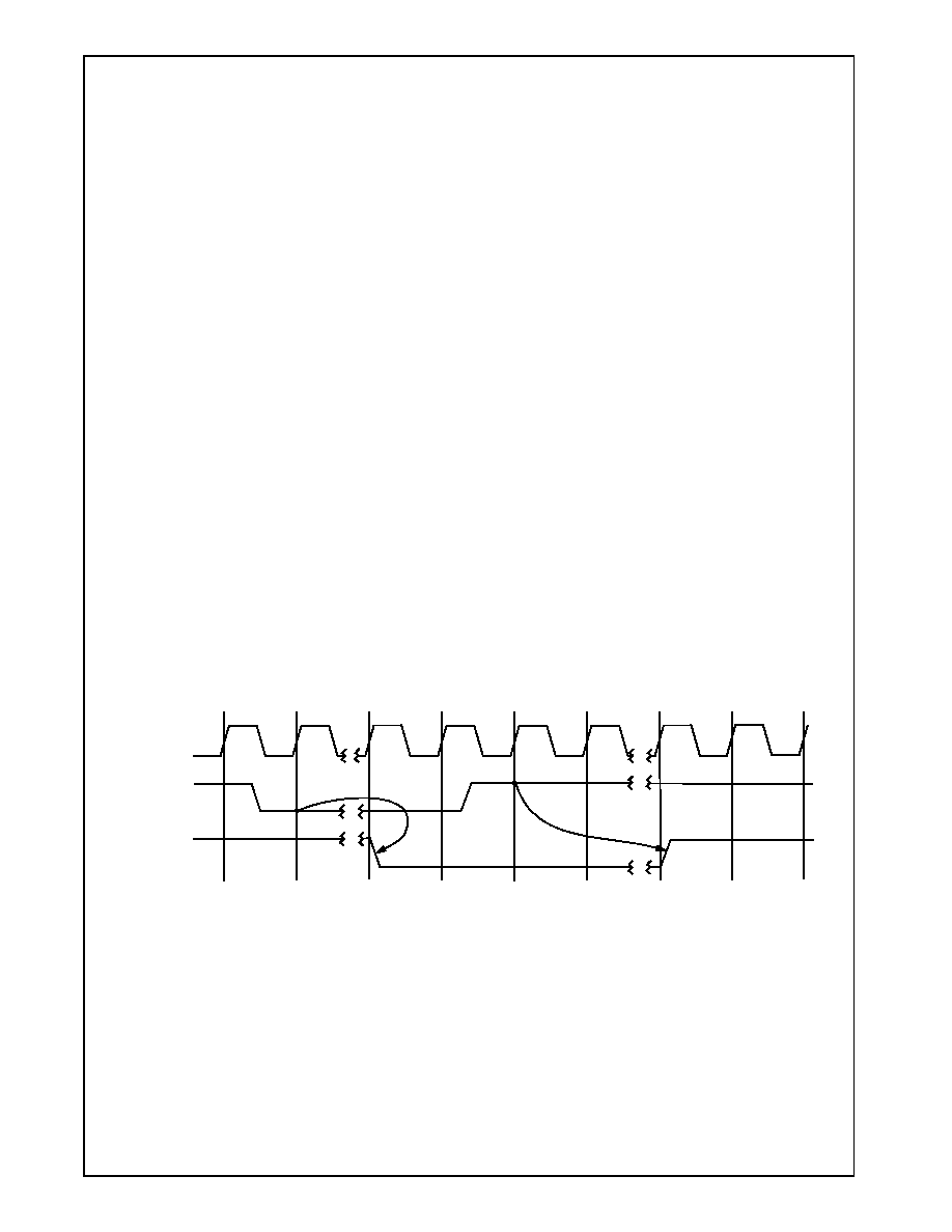
Revision 3.1
175
www.national.com
Power Management (
Continued
)
GeodeTM
G
Xm
P
r
ocessor
selected by setting bit 0 in the PM Clock Stop Control
Register. If you are using DRAMs without self refresh, you
must supply a 32 kHz clock to the CLK32KHZ bit to keep
the refresh circuitry active when using the lower-power
Suspend mode.
While also in 3-Volt Suspend Mode, the CS5530 contin-
ues to decrement all of its device timers, and it responds
to external SMI interrupts using the 32 kHz clock input
(CLK32KHz) pin. Any SMI event, timer or pin, causes the
CS5530 to deassert the SUSP_3V pin, starting the sys-
tem clocks. The CS5530 holds SUSP# active for a pre-
programmed period that varies from 0 to 16 ms, which
allows the clocks to settle. After this period expires, the
CS5530 deasserts SUSP#. SMI# is held active for the
entire period, so that the GXm processor status registers
are updated.
The SUSP_3V pin can be active either high or low. The
pin is an input during POR, and is sampled to determine
its inactive state. This allows a designer to match the
active state of SUSP_3V to the inactive state for a clock
driver output enable with a pull-up or pull-down resistor.
6.5
SUSPEND MODE AND BUS CYCLES
The following subsections describe the bus cycles when
the Suspend mode is implemented.
6.5.1
Initiating Suspend with SUSP#
The GXm processor has two low-power Suspend modes.
The mode is selected by bit 0 in the PM Clock Stop Con-
trol Register. One mode (bit 0 cleared) turns off the inter-
nal clocks to everything but the internal Display and
Memory Controllers, keeping the display active. A lower-
power mode turns off all internal clocks generated from
SYSCLK. This mode is selected by setting bit 0 in the PM
Clock Stop Control Register. If the bit is set and DRAMS
without self-refresh are used, a 32 KHz clock must be
supplied to the CLK32KHZ input to keep the refresh circuit
active.
The GXm processor enters the Suspend mode in
response to SUSP# input assertion only when certain
conditions are met. First, the USE_SUSP bit must be set
in CCR2 (Index C2h[7]). In addition, execution of the cur-
rent instructions and any pending decoded instructions
and associated bus cycles must be completed. SUSP# is
sampled on the rising edge of SYSCLK, and must meet
specified setup and hold times to be recognized at a par-
ticular SYSCLK edge.
When all conditions are met, the SUSPA# output is
asserted. The time from assertion of SUSP# to the activa-
tion of SUSPA# depends on which instructions were
decoded prior to assertion of SUSP#. Normally, once
SUSP# has been sampled inactive the SUSPA# output
will be deactivated within two clocks. However, the deacti-
vation of SUSPA# may be delayed until the end of an
active refresh cycle.
If the CPU is already in a Suspend mode initiated by
SUSP#, one occurrence of NMI, INTR and SMI# is stored
for execution after Suspend mode is exited. The CPU also
allows PCI accesses during a SUSP#-initiated Suspend
mode (see Figure 6-1). If the CPU is in the middle of a
PCI access when SUSP# is asserted, the assertion of
SUSPA# will be delayed until the PCI access is com-
pleted.
Figure 6-1. SUSP#-Initiated Suspend Mode
SYSCLK
SUSP#
SUSPA#

www.national.com
176
Revision 3.1
Power Management (
Continued
)
GeodeTM
G
Xm
Pr
ocessor
6.5.2
Initiating Suspend with HALT
The CPU also enters Suspend mode as a result of execut-
ing a HALT instruction if the SUSP_HALT bit in CCR2
(Index C2h[3]) is set. Suspend mode is then exited upon
recognition of an NMI, an unmasked INTR, or an SMI#.
Normally SUSPA# is deactivated within six SYSCLKS
from the detection of an active interrupt. However, the
deactivation of SUSPA# may be delayed until the end of
an active refresh cycle.
The CPU also allows PCI accesses during a HALT-initi-
ated Suspend mode. If the CPU is in the middle of a PCI
access when the Halt instruction is executed, the asser-
tion of SUSPA# will be delayed until the PCI access is
completed.
Figure 6-2. HALT-Initiated Suspend Mode
SYSCLK
FRAME#
C/BE[3:0]#
AD[15:0]
IRDY#
INTR, NMI,
SUSPA#
O
X
I
I
X
X
SMI#
HALT
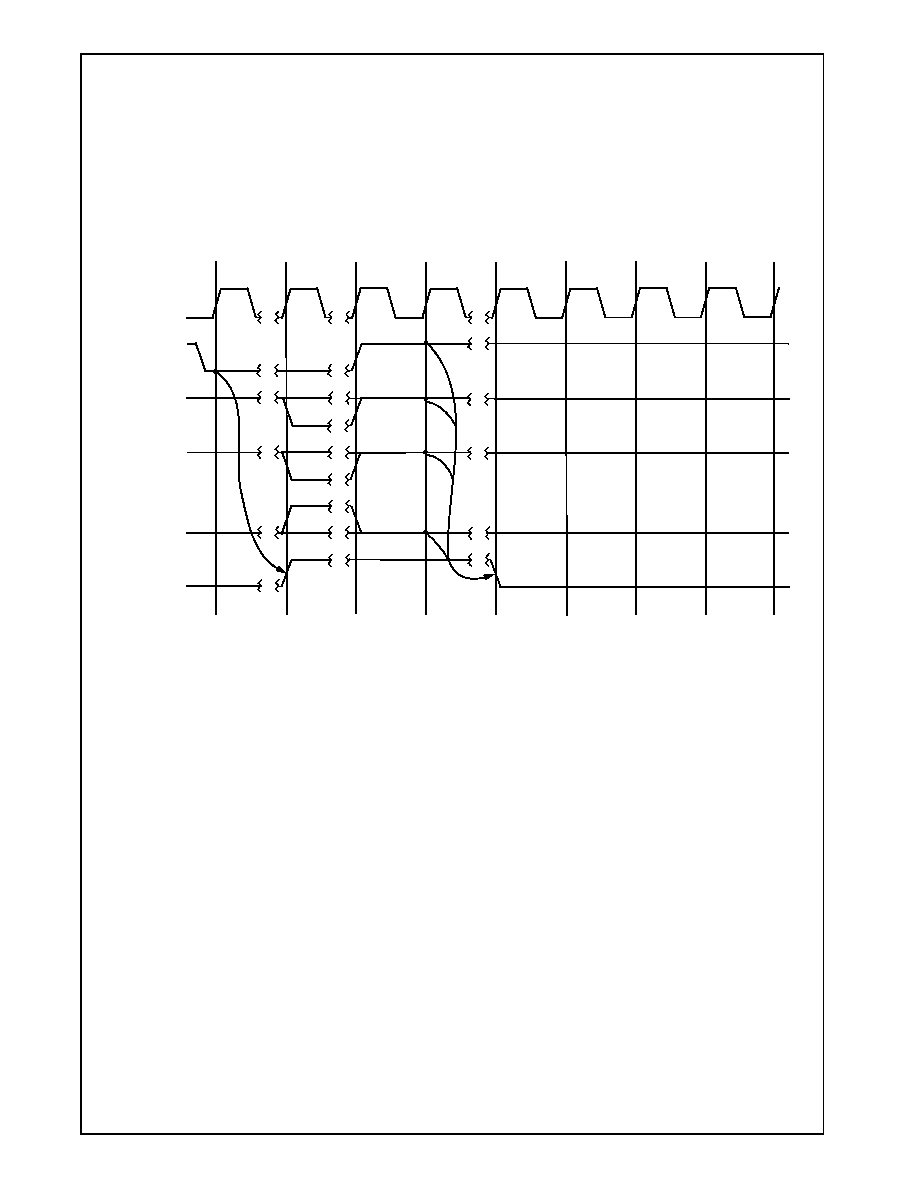
Revision 3.1
177
www.national.com
Power Management (
Continued
)
GeodeTM
G
Xm
P
r
ocessor
6.5.3
Responding to a PCI Access During Suspend
Mode
The GXm processor can temporarily exit Suspend mode
to handle PCI accesses. If an unmasked REQx# is
asserted, the GXm processor will deassert SUSPA# and
exit the Suspend mode to respond to the PCI access. A
PCI access is completed when FRAME# is inactive and
TRDY# or STOP# are active. If SUSP# is asserted when
the PCI access is completed, the GXm processor will
assert SUSPA# and return to a SUSP#-initiated Suspend
mode. If it was a HALT-initiated Suspend mode and no
active interrupts have been recognized, the CPU will
assert SUSPA# and return to a HALT-initiated Suspend
mode.
Figure 6-3. PCI Access During Suspend Mode
SYSCLK
REQx#
TRDY#
SUSP#
SUSPA#
FRAME#
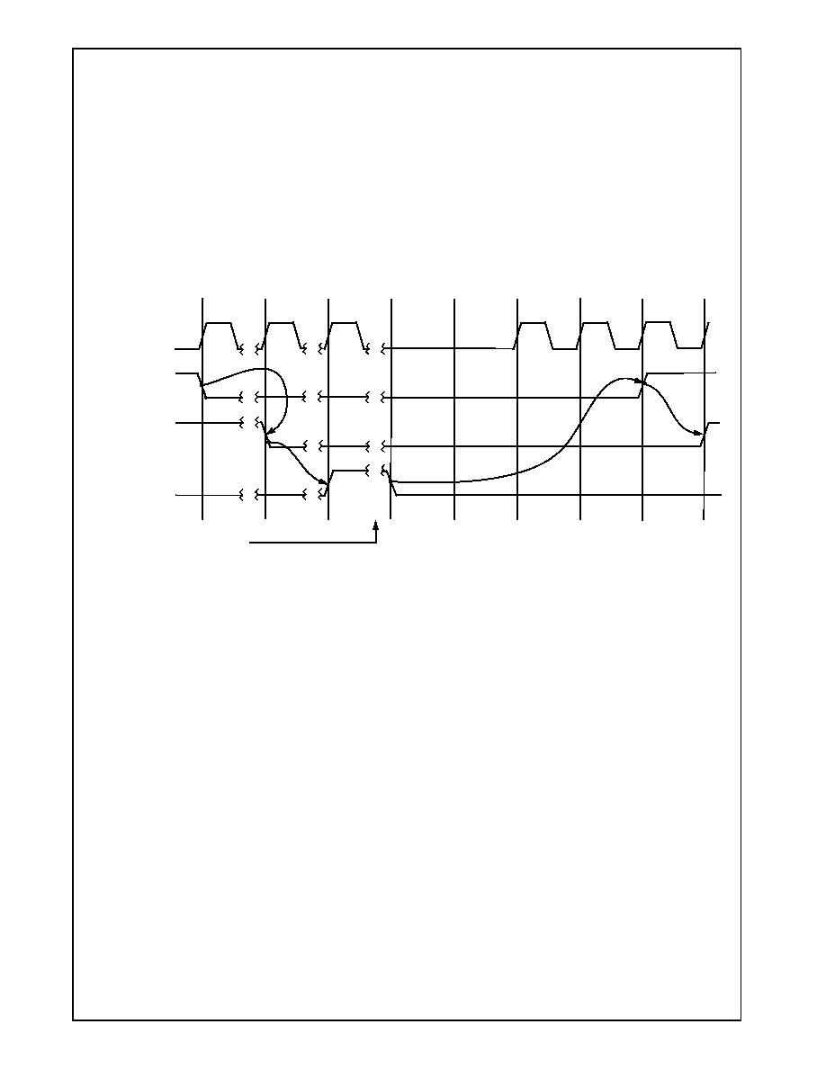
www.national.com
178
Revision 3.1
Power Management (
Continued
)
GeodeTM
G
Xm
Pr
ocessor
6.5.4
Stopping the Input Clock
Because the GXm processor is a static device, the input
clock (SYSCLK) can be stopped and restarted without
any loss of internal CPU data. If DRAMS are used that do
not have self-refresh, bit 0 of the PM Clock Stop Control
Register must be set to a one and the CLK32KHZ input
must be continuously applied to keep the refresh circuitry
running. The SYSCLK input can be stopped at either a
logic high or logic low state. The required sequence for
stopping SYSCLK is to initiate CPU Suspend mode, wait
for the assertion of SUSPA# by the processor, and then
stop the input clock.
The CPU remains suspended until SYSCLK is restarted
and the Suspend mode is exited as described earlier.
While SYSCLK is stopped, the processor can no longer
sample and respond to any input stimulus including
REQx#, NMI, SMI#, INTR, and RESET inputs.
Figure 6-4 illustrates the recommended sequence for
stopping the SYSCLK using SUSP# to initiate Suspend
mode. SYSCLK may be started prior to or following nega-
tion of the SUSP# input. The figure includes the
SUSP_3V pin from the CS5530 which is used to stop the
external clocks.
Figure 6-4. Stopping SYSCLK During Suspend Mode
SYSCLK
SUSP#
SUSP_3V
SMI Event, Timer or Pin
SUSPA#
(CS5530)
Revision 3.1
179
www.national.com
Power Management (
Continued
)
GeodeTM
G
Xm
P
r
ocessor
6.6
GXM PROCESSOR SERIAL BUS
The power management logic of the GXm processor pro-
vides the CS5530 with information regarding the GXm
processor productivity. If the GXm processor is deter-
mined to be relatively inactive, the GXm processor power
consumption can be greatly reduced by entering the Sus-
pend Modulation mode.
Although the majority of the system power management
logic is implemented in the CS5530, a small amount of
logic is required within the GXm processor to provide
information from the graphics controller that is not exter-
nally visible otherwise. The GXm processor implements a
simple serial communications mechanism to transmit the
CPU status to the CS5530. The GXm processor accumu-
lates CPU events in a 8-bit register, "PM Serial Packet
Register" (GX_BASE+850Ch, see Table 6-1), which is
serially transmitted out of the GXm processor every 1 to
10 µs. The transmission frequency is set with the "PM
Serial Packet Control Register" (GX_BASE+8504h, see
Table 6-1).
6.6.1
Serial Packet Transmission
The GXm processor transmits the contents of the "PM
Serial Packet Register" on the SERIALP output pin to the
PSERIAL input pin of the CS5530. The GXm processor
holds SERIALP low until the transmission interval counter
(GX_BASE+8504h[4:3]) has elapsed. Once the counter
has elapsed, PSERIAL is held high for two SYSCLKs to
indicate the start of packet transmission. The contents of
the packet register are then shifted out starting from bit 7
down to bit 0. PSERIAL is held high for one SYSCLK to
indicate the end of packet transmission and then remains
low until the next transmission interval. After the packet
transmission has completed, the packet contents are
cleared.
6.7
POWER MANAGEMENT REGISTERS
The GXm processor contains the power management
registers for the serial packet transmission control, the
user-defined power management address space, Sus-
pend Refresh, and SMI status for Suspend/Resume.
These registers are memory mapped (GX_BASE+8500h-
8FFFh) in the address space of the GXm processor and
are described in the following sections. Refer to Section
4.1.2 "Control Registers" on page 94 for instructions on
accessing these registers.
Note, however, the PM_BASE and PM_MASK registers
are accessed with the CPU_READ and CPU_WRITE
instructions.
Refer
to
Section
4.1.6
"CPU_READ/CPU_WRITE Instructions" on page 99 for
more information regarding these instructions.
Table 6-1 summarizes the above mentioned registers.
Tables 6-2 and 6-3 starting on page 180 give these regis-
ter's bit formats.
Table 6-1. Power Management Register Summary
GX_BASE+
Memory Offset
Type
Name/Function
Default Value
Control and Status Registers
8500h-8503h
R/W
PM_STAT_SMI
PM SMI Status Register -- Contains System Management Mode (SMM) status
information used by SoftVGA.
xxxxxx00h
8504h-8507h
R/W
PM_CNTRL_TEN
PM Serial Packet Control Register -- Sets the serial packet transmission frequency
and enables specific CPU events to be recorded in the serial packet.
xxxxxx00h
8508h-850Bh
R/W
PM_CNTRL_CSTP
PM Clock Stop Control Register -- Enables the 3-V Suspend Mode for the GXm
processor.
xxxxxx00h
850Ch-850Fh
R/W
PM_SER_PACK
PM Serial Packet Register -- Transmits the contents of the serial packet.
xxxxxx00h
Programmable Address Region Registers
FFFF FF6Ch
R/W
PM_BASE
PM Base Register -- Contains the base address for the programmable memory
range decode. This register, in combination with the PM_MASK register, is used to
generate a memory range decode which sets bit 1 in the serial transmission packet.
00000000h
FFFF FF7Ch
R/W
PM_MASK
PM Mask Register -- The address mask for the PM_BASE register
00000000h
www.national.com
180
Revision 3.1
Power Management (
Continued
)
GeodeTM
G
Xm
Pr
ocessor
Table 6-2. Power Management Control and Status Registers
Bit
Name
Description
GX_BASE+8500h-8503h
PM_STAT_SMI Register (R/W)
Default Value = xxxxxx00h
31:8
RSVD
Reserved -- These bits are not used. Do not write to these bits.
7:3
RSVD
Reserved -- Set to 0.
2
SMI_MEM
SMI VGA Emulation Memory -- This bit is set high if a SMI was generated for VGA emulation in
response to a VGA memory access. An SMI can be generated on a memory access to one of three
regions in the A0000h-to-BFFFFh range as specified in the BC_XMAP_1 register.
1
SMI_IO
SMI VGA Emulation I/O -- This bit is set high if a SMI was generated for VGA emulation in
response to an I/O access. An SMI can be generated on a I/O access to one of three regions in the
3B0h-to-3DFh range as specified in the BC_XMAP_1 register.
0
SMI_PIN
SMI Pin -- When set high, this bit indicates that the SMI# input pin has been asserted to the
GXm processor.
Note: These bits are "sticky" bits and can only be cleared with a write of `1' to the respective bit.
GX_BASE+8504h-8507h
PM_CNTRL_TEN Register (R/W)
Default Value = xxxxxx00h
31:8
RSVD
Reserved -- These bits are not used. Do not write to these bits.
7:6
RSVD
Reserved -- Set to 0.
5
X_TEST (WO)
Transmission Test (Write Only) -- Setting this bit causes the GXm processor to immediately trans-
mit the current contents of the serial packet. This bit is write only and is used primarily for test. This
bit returns 0 on a read.
4:3
X_FREQ
Transmission Frequency -- This field indicates the time between serial packet transmissions.
Serial packet transmissions occur at the selected interval only if at least one of the packet bits is set
high: 00 = Disable transmitter; 01 = 1 ms; 10 = 5 ms; 11 = 10 ms.
2
CPU_RD
CPU Activity Read Enable -- Setting this bit high enables reporting of CPU Level-1 cache read
misses that are not a result of an instruction fetch. This bit is a don't-care if the CMEN bit is not set
high
1
CPU_EN
CPU Activity Master Enable -- Setting this bit high enables reporting of CPU Level-1 cache
misses in bit 6 of the serial transmission packet. When enabled, the CPU Level-1 cache miss activity
is reported on any read (assuming the CREN is set high) or write access excluding misses that
resulted from an instruction fetch.
0
VID_EN
Video Event Enable -- Setting this bit high enables video decode events to be reported in bit 0 of
the serial transmission packet. CPU or graphics-pipeline accesses to the graphics memory and dis-
play-controller-register accesses are also reported.
GX_BASE+8508h-850Bh
PM_CNTRL_CSTP Register (R/W)
Default Value = xxxxxx00h
31:8
RSVD
Reserved -- These bits are not used. Do not write to these bits.
7:1
RSVD
Reserved -- Set to 0.
0
CLK_STP
Clock Stop -- This bit configures the GXm processor for Suspend Refresh Mode or 3-Volt Suspend
Mode:
0 = Suspend Refresh Mode. The clocks to the memory and display controller are active.
1 = 3-Volt Suspend Mode. All internal clocks are stopped.
Note: When this register is set high and the Suspend input pin (SUSP#) is asserted, the GXm processor stops all it's internal clocks,
and asserts the Suspend Acknowledge output pin (SUSPA#). Once SUSPA# is asserted the GXm processor's SYSCLK input
can be stopped. If this register is cleared, the internal memory-controller and display-controller clocks are not stopped on the
SUSP#/SUSPA# sequence, and the SYSCLK input can not be stopped.
GX_BASE+850Ch-850Fh
PM_SER_PACK Register (R/W)
Default Value = xxxxxx00h
31:8
RSVD
Reserved -- These bits are not used. Do not write to these bits.
7
VID_IRQ
Video IRQ -- This bit indicates the occurrence of a video vertical sync pulse. This bit is set at the
same timer that the VINT (Vertical Interrupt) bit is set in the DC_TIMING_CFG register. The VINT bit
has a corresponding enable bit (VIEN) in the DC_TIM_CFG register.
6
CPU_ACT
CPU Activity -- This bit indicates the occurrence of a level 1 cache miss that was not a result of an
instruction fetch. This bit has a corresponding enable bit in the PM_CNTL_TEN register.
5:2
RSVD
Reserved -- Set to 0.
1
USR_DEF
Programmable Address Decode -- This bit indicates the occurrence of a programmable memory
address decode. This bit is set based on the values of the PM_BASE register and the PM_MASK
register. The PM_BASE register can be initialized to any address in the full 128 MB address range.
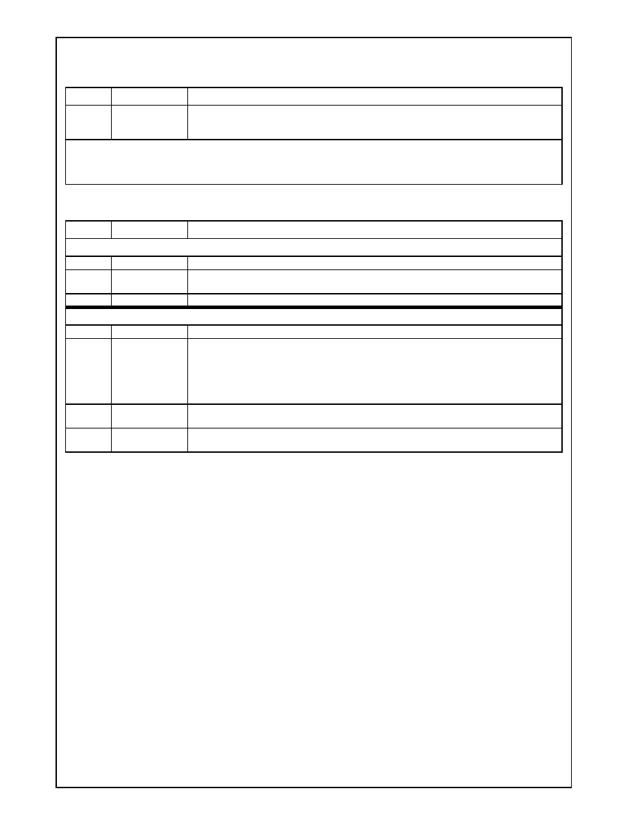
Revision 3.1
181
www.national.com
Power Management (
Continued
)
GeodeTM
G
Xm
P
r
ocessor
0
VID_DEC
Video Decode -- This bit indicates that the CPU has accessed either the Display Controller regis-
ters or the graphics memory region. This bit has a corresponding enable bit in the
PM_CNTRL_TEN.
Note: The GXm processor transmits the contents of the serial packet only when a bit in the packet register is set and the interval
counter has elapsed. The CS5530 decodes the serial packet after each transmission. Once a bit in the packet is set, it will
remain set until the completion of the next packet transmission. Successive events of the same type that occur between packet
transmissions are ignored. Multiple unique events between packet transmissions will accumulate in this register.
Table 6-2. Power Management Control and Status Registers (Continued)
Bit
Name
Description
Table 6-3. Power Management Programmable Address Region Registers
Bit
Name
Description
Index FFFFFF6Ch
PM_BASE Register (R/W)
Default Value = 0000000h
31:28
RSVD
Reserved -- Set to 0.
27:2
BASE_ADDR
Base Address -- This is the word-aligned base address for the programmable memory range com-
pare. The actual address range is determined with this field and the PM_MASK register value.
1:0
RSVD
Reserved -- Set to 0.
Index FFFFFF7Ch
PM_MASK Register (R/W)
Default Value = 0000000h
31:28
RSVD
Reserved -- Set to 0.
27:2
ADR_MASK
Address Mask -- This field is the address mask for the BASE_ADDR field in the PM_BASE regis-
ter. If a bit in the ADR_MASK field is cleared the corresponding bit in the BASE_ADDR field must
match the processor address. If a bit in the mask field is set high, the corresponding bit in the
BASE_ADDR field always compares. If the processor cycle type matches the values of the WE and
RE bits, and all bits in the BADD field match the processor address based on the ADR_MASK field,
bit 1 will be set high in the serial transmission packet.
1
WE
Write Enable -- Compare memory write cycles with BASE_ADDR and ADR_MASK:
0 = Disable; 1 = Enable.
0
RE
Read Enable -- Compare memory read cycles with BASE_ADDR and ADR_MASK:
0 = Disable; 1 = Enable

www.national.com
182
Revision 3.1
GeodeTM
G
Xm
Pr
ocessor
7.0
Electrical Specifications
This section provides information on electrical connec-
tions, absolute maximum ratings, required operating con-
ditions, DC characteristics, and AC characteristics for the
Geode GXm processor. All voltage values in the Electrical
Specifications are with respect to V
SS
unless otherwise
noted. For detailed information on the PCI bus electrical
specification refer to Chapter 4 of the PCI Bus Specifica-
tion, Revision 2.1.
7.1
PART NUMBERS
The following part numbers designate the various speeds
available. For all speeds, the V
CC2
voltage is 2.9V nominal
and the V
CC3
voltage is 3.3V nominal.
7.2
ELECTRICAL CONNECTIONS
7.2.1
Power/Ground Connections and Decoupling
Testing and operating the GXm processor requires the
use of standard high frequency techniques to reduce par-
asitic effects. These effects can be minimized by filtering
the DC power leads with low-inductance decoupling
capacitors, using low-impedance wiring, and by utilizing
all of the V
CC2
, V
CC3
, and VSS pins.
7.2.2
Power Sequencing
the Core and I/O Voltages
With two voltages connected to the GXm processor, it is
important that the voltages come up in the correct order.
V
CC2
should come up at or before V
CC3
. There are no
additional timing requirements related to this sequence.
7.2.3
NC-Designated Pins
Pins designated NC (No Connection) should be left dis-
connected. Connecting an NC pin to a pull-up/-down
resistor, or an active signal could cause unexpected
results and possible circuit malfunctions.
7.2.4
Pull-Up and Pull-Down Resistors
Table 7-2 lists the input pins that are internally connected
to a 20-kohm pull-up/-down resistor. When unused, these
inputs do not require connection to an external pull-up/-
down resistor.
7.2.5
Unused Input Pins
All inputs not used by the system designer and not listed
in Table 7-2 should be kept at either ground or V
CC3
. To
prevent possible spurious operation, connect active-high
inputs to ground through a 20-kohm (±10%) pull-down
resistor and active-low inputs to V
CC3
through a 20-kohm
(±10%) pull-up resistor.
Table 7-1. Part Numbers
Core
Frequency
(MHz)
Temperature
(Degree C)
Part Marking
266
70
GXm-266P 2.9V 70C
85
GXm-266P 2.9V 85C
70
GXm-266B 2.9V 70C
85
GXm-266B 2.9V 85C
233
70
GXm-233P 2.9V 70C
85
GXm-233P 2.9V 85C
70
GXm-233B 2.9V 70C
85
GXm-233B 2.9V 85C
200
70
GXm-200P 2.9V 70C
85
GXm-200P 2.9V 85C
70
GXm-200B 2.9V 70C
85
GXm-200B 2.9V 85C
180
70
GXm-180P 2.9V 70C
85
GXm-180P 2.9V 85C
70
GXm-180B 2.9V 70C
85
GXm-180B 2.9V 85C
Note:
B = BGA Package
P = SPGA Package
Table 7-2. Pins with 20-kohm
Internal Resistor
Signal Name
BGA
Ball No.
SPGA
Pin No.
PU/PD
SUSP#*
H2
M4
Pull-up
FRAME#
A8
C13
Pull-up
IRDY#
C9
D14
Pull-up
TRDY#
B9
B14
Pull-up
STOP#
C11
A15
Pull-up
LOCK#
B11
B16
Pull-up
DEVSEL#
A9
E15
Pull-up
PERR#
A11
D16
Pull-up
SERR#
C12
A17
Pull-up
REQ[2:0]#
D3,
H3,
E3
E3,
K2,
E1
Pull-up
TCLK
J2
P4
Pull-up
TMS
H1
N3
Pull-up
TDI
D2
F4
Pull-up
TEST
F3
J5
Pull-down
Note:
*SUSP# is pulled up when not active.

Revision 3.1
183
www.national.com
Electrical Specifications (
Continued
)
GeodeTM
G
Xm
P
r
ocessor
7.3
ABSOLUTE MAXIMUM RATINGS
Table 7-3 lists absolute maximum ratings for the GXm pro-
cessor. Stresses beyond the listed ratings may cause per-
manent damage to the device. Exposure to conditions beyond
these limits may (1) reduce device reliability and (2) result
in premature failure even when there is no immediately
apparent sign of failure. Prolonged exposure to conditions
at or near the absolute maximum ratings may also result
in reduced useful life and reliability. These are stress rat-
ings only and do not imply that operation under any condi-
tions other than those listed under Table 7-4 on page 184
is possible.
Table 7-3. Absolute Maximum Ratings
Parameter
Min
Max
Units
Notes
Operating Case Temperature
≠65
110
∞C
Power Applied
Storage Temperature
≠65
150
∞C
No Bias
Supply Voltage
3.2
V
Voltage On Any Pin
≠0.5
6.0
V
Input Clamp Current, I
IK
≠0.5
10
mA
Power Applied
Output Clamp Current, I
OK
25
mA
Power Applied
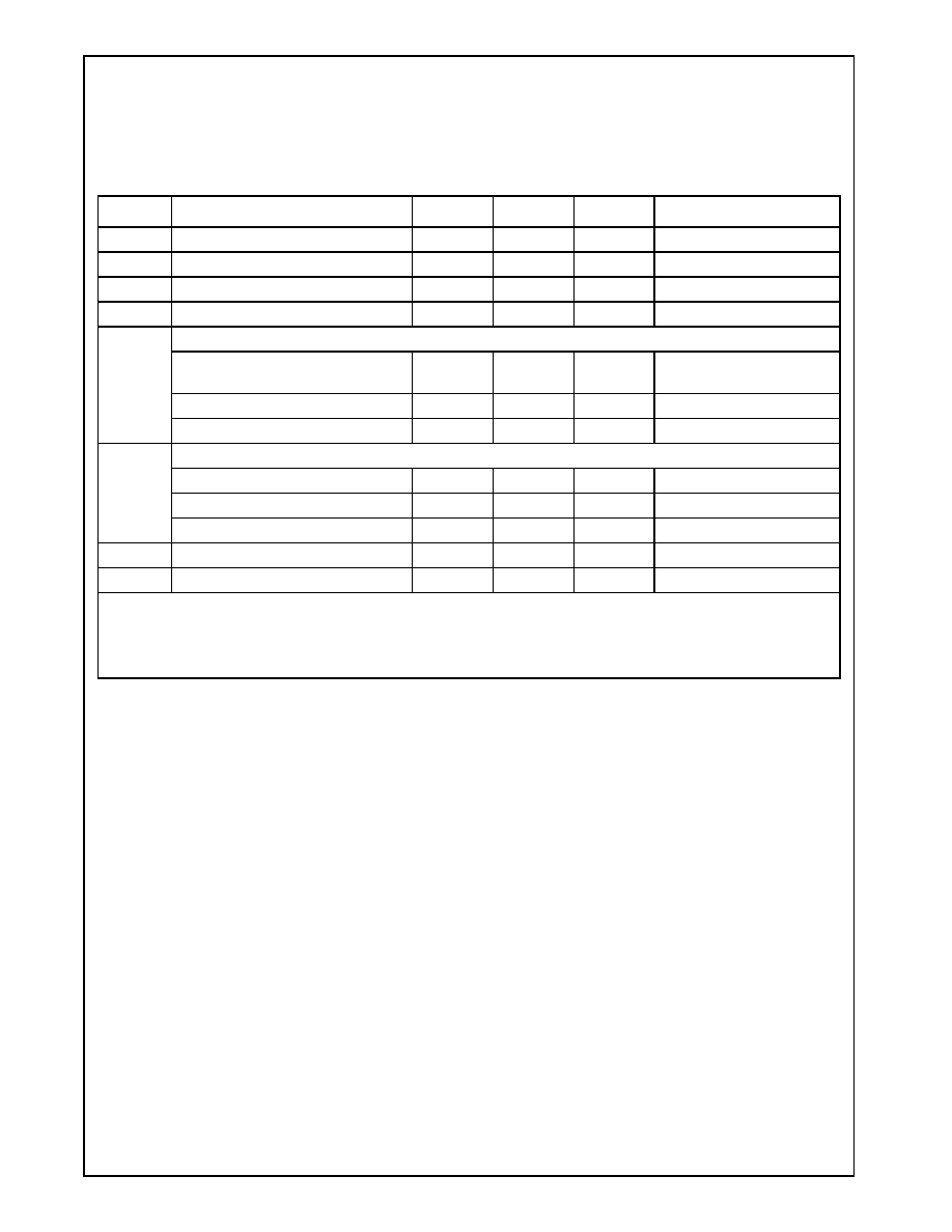
www.national.com
184
Revision 3.1
Electrical Specifications (
Continued
)
GeodeTM
G
Xm
Pr
ocessor
7.4
OPERATING CONDITIONS
Table 7-4 lists the operating conditions for the GXm processor.
Table 7-4. Operating Conditions
Symbol
Parameter
Min
Max
Units
Notes
T
C
Operating Case Temperature
0
70
∞C
For Desktop Applications
T
C
Operating Case Temperature
0
85
∞C
For Notebook Applications
V
CC2
Supply Voltage (2.9V nominal)
2.75
3.05
V
V
CC3
Supply Voltage (3.3V nominal)
3.14
3.46
V
V
IH
High-Level Input Voltage:
All input and I/O pins except
SDRAM Interface and SYSCLK
2.0
5.5
V
Note 1
SDRAM Interface
2.0
V
CC3
+0.5
V
Note 2
SYSCLK
2.7
5.5
V
Note 1
V
IL
Low-Level Input Voltage:
All except PCI bus and SYSCLK
≠0.5
0.8
V
PCI bus
≠0.5
0.3*V
CC3
V
SYSCLK
≠0.5
0.4
V
I
OH
High-Level Output Current
≠2
mA
V
O
= V
OH
(Min)
I
OL
Low-Level Output Current
5
mA
V
O
= V
OL
(Max)
Notes: 1) This parameter indicates that these pins are tolerant to the PCI 5 Volt Signaling Environment DC
specification.
2) SDRAM Interface Pins: BA[1:0], CAS[A:B]#, CKE[A:B], CS[3:0]#, DQM[7:0], MA[12:0], MD[63:0], RASA#,
RASB#, SDCLK_IN, SDCLK_OUT, SDCLK[3:0], TEST[3:0], WE[A:B]#

Revision 3.1
185
www.national.com
Electrical Specifications (
Continued
)
GeodeTM
G
Xm
P
r
ocessor
7.5
DC CHARACTERISTICS
DC characteristics were measured under the operating conditions listed in Table 7-4 on page 184.
Table 7-5. DC Characteristics
Symbol
Parameter
Min
Max
Units
Notes
V
OL
Output Low Voltage
0.4
V
I
OL
= 5 mA
V
OH
Output High Voltage
2.4
V
I
OH
= ≠2 mA
I
I
Input Leakage Current for all input pins except
those with internal PU/PDs
±10
µ
A
0 < V
IN
< V
CC3
,
See Table 7-2
I
IH
Input Leakage Current for all pins with
internal PDs.
200
µ
A
V
IH
= 2.4 V,
See Table 7-2
I
IL
Input Leakage Current for all pins with
internal PUs.
≠400
µ
A
V
IL
= 0.35 V,
See Table 7-2
I
CC
Active I
CC
:
Core I
CC
2 at f
CLK
= 180 MHz
I/O I
CC
3 at f
CLK
= 180 MHz
2.25
0.400
A
Note 1
Core I
CC
2 at f
CLK
= 200 MHz
I/O I
CC
3 at f
CLK
= 200 MHz
2.55
0.405
Core I
CC
2 at f
CLK
= 233 MHz
I/O I
CC
3 at f
CLK
= 233M Hz
2.85
0.410
Core I
CC
2 at f
CLK
= 266 MHz
I/O I
CC
3 at f
CLK
= 266 MHz
3.10
0.415
I
CCSM
Suspend Mode I
CC
:
Core I
CC
2 at f
CLK
= 180 MHz
I/O I
CC
3 at f
CLK
= 180 MHz
18
8
mA
Notes 1 and 4
Core I
CC
2 at f
CLK
= 200 MHz
I/O I
CC
3 at f
CLK
= 200 MHz
22
9
Core I
CC
2 at f
CLK
= 233 MHz
I/O I
CC
3 at f
CLK
= 233 MHz
25
10
Core I
CC
2 at f
CLK
= 266 MHz
I/O I
CC
3 at f
CLK
= 266 MHz
28
11
I
CCSS
Standby I
CC
(Suspend and CLK Stopped):
Core I
CC
2 at f
CLK
= 0 MHz
I/O I
CC
3 at f
CLK
= 0 MHz
10
5
mA
Notes 1 and 3
C
IN
Input Capacitance
16
pF
f = 1 MHz, Note 2
C
OUT
Output or I/O Capacitance
16
pF
f = 1 MHz, Note 2
C
CLK
CLK Capacitance
12
pF
f = 1 MHz, Note 2
Notes:
1.
fCLK ratings refer to internal clock frequency.
2.
Not 100% tested.
3.
All inputs are at 0.2 V or VCC3 ≠ 0.2 (CMOS levels). All inputs are held static and all outputs are unloaded
(static IOUT = 0 mA).
4.
All inputs are at 0.2 V or VCC3 ≠ 0.2 (CMOS levels). All inputs except clock are held static and all outputs are unloaded
(static IOUT = 0 mA).

www.national.com
186
Revision 3.1
Electrical Specifications (
Continued
)
GeodeTM
G
Xm
Pr
ocessor
7.6
AC CHARACTERISTICS
The following tables list the AC characteristics including
output delays, input setup requirements, input hold
requirements and output float delays. The rising-clock-
edge reference level V
REF
, and other reference levels are
shown in Table 7-6.
Input or output signals must cross
these levels during testing.
Input setup and hold times are specified minimums that
define the smallest acceptable sampling window for which
a synchronous input signal must be stable for correct oper-
ation.
All AC tests are at V
CC2
= 2.75V to 3.05V (2.9V nominal),
T
C
= 0
o
C to 70
o
C or 85
o
, C
L
= 50 pF unless otherwise
specified.
Figure 7-1. Drive Level and Measurement Points for Switching Characteristics
Table 7-6. Drive Level and Measurement Points
for Switching Characteristics
Symbol
Voltage (V)
V
REF
1.5
V
IHD
2.4
V
ILD
0.4
CLK
OUTPUTS
INPUTS
V
IHD
V
ILD
V
REF
Valid Input
Valid Output
n+1
Valid Output
n
V
REF
V
REF
V
ILD
V
IHD
Min
Max
Legend: A = Maximum Output Delay Specification
B = Minimum Output Delay Specification
C = Minimum Input Setup Specification
D = Minimum Input Hold Specification
T
X
B
A
C
D

Revision 3.1
187
www.national.com
Electrical Specifications (
Continued
)
GeodeTM
G
Xm
P
r
ocessor
Figure 7-1 SYSCLK Timing and Measurement Points
Table 7-7. Clock Signals
Symbol
ParameterT
180 MHz (6x)
(Note)
200 MHz (6x)
(Note)
233 MHz (7x)
(Note)
266 MHz (8x)
(Note)
Units
Min
Max
Min
Max
Min
Max
Min
Max
t1
SYSCLK Period
33.3
30.0
30.0
30.0
ns
t2
SYSCLK Period Stability
±250
±250
±250
±250
ps
t3
SYSCLK High Time
10
10
10
10
ns
t4
SYSCLK Low Time
10
10
10
10
ns
t5
SYSCLK Fall Time
0.15
2.0
0.15
2.0
0.15
2.0
0.15
2.0
ns
t6
SYSCLK Rise Time
0.15
2.0
0.15
2.0
0.15
2.0
0.15
2.0
ns
t7
DCLK Period
7.3
7.3
7.3
7.3
ns
t8
DCLK Rise/Fall Time
3.0
3.0
3.0
3.0
ns
t9
SDCLK_OUT,
SDCLK[3:0] Period
14.5
19.5
13
17
11
16
10
13
ns
t10
SDCLK_OUT,
SDCLK[3:0] High Time
7.5
6.5
5.5
5
ns
t11
SDCLK_OUT,
SDCLK[3:0] Low Time
7.5
6.5
5.5
5
ns
t12
SDCLK_OUT,
SDCLK[3:0] Fall Time
0.15
2.0
0.15
2.0
0.15
2.0
0.15
2.0
ns
t13
SDCLK_OUT,
SDCLK[3:0] Rise Time
0.15
2.0
0.15
2.0
0.15
2.0
0.15
2.0
ns
Note: SDCLK timings (t9-t13) assume an SDCLK that is a "divide by 3" from the internal core clock. Hence:
180 MHz (6x) = 60.0 MHz SDCLK
200 MHz (6x) = 66.7 MHz SDCLK
233 MHz (7x) = 77.7 MHz SDCLK
266 MHz (8x) = 88.7 MHz SDCLK
SYSCLK
1.5V
V
IH (Min)
V
IL (Max)
t3
t1
t6
t5
t4
www.national.com
188
Revision 3.1
Electrical Specifications (
Continued
)
GeodeTM
G
Xm
Pr
ocessor
Figure 7-2. DCLK Timing and Measurement Points
Figure 7-3. SDCLK, SDCLK[3:0] Timing and Measurement Points
Table 7-8. System Signals
DCLK
t8
t7
SDCLK,
1.5V
V
IH (Min)
V
IL (Max)
t10
t9
t13
t12
t11
SDCLK[3:0]
Parameter
Min
Max
Unit
Notes
Setup Time for RESET, INTR
5
ns
Note
Hold Time for RESET, INTR
2
ns
Note
Setup Time for SMI#, SUSP#, FLT#
5
ns
Hold Time for SMI#, SUSP#, FLT#
2
ns
Valid Delay for IRQ13, SUSPA#
2
15
ns
Valid Delay for SERIALP
2
15
ns
Note:
The system signals may be asynchronous. The setup/hold times are required for determining static
behavior.
Revision 3.1
189
www.national.com
Electrical Specifications (
Continued
)
GeodeTM
G
Xm
P
r
ocessor
Table 7-9. PCI Interface Signals
Figure 7-4. Output Timing
Figure 7-5. Input Timing
Symbol
Parameter
Min
Max
Unit
Notes
t
VAL1
Delay Time, SYSCLK to Signal Valid for Bused
Signals
2
11
ns
t
VAL2
Delay Time, SYSCLK to Signal Valid for GNT#
2
12
ns
Note
t
ON
Delay Time, Float to Active
2
ns
t
OFF
Delay Time, Active to Float
28
ns
t
SU1
Input Setup Time for Bused Signals
7
ns
t
SU2
Input Setup Time for REQ#
12
ns
Note
t
H
Input Hold Time to SYSCLK
0
ns
Note:
GNT# and REQ# are point-to-point signals. All other PCI interface signals are bused.
Refer to Chapter 4 of PCI Local Bus Specification, Revision 2.1, for more detailed information.
SYSCLK
TRISTATE
OUTPUT
OUTPUT
t
VAL1,2
t
OFF
t
ON
SYSCLK
INPUT
t
H
t
SU1,2
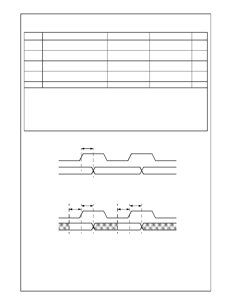
www.national.com
190
Revision 3.1
Electrical Specifications (
Continued
)
GeodeTM
G
Xm
Pr
ocessor
Table 7-10. SDRAM Interface Signals
Figure 7-6. Output Valid Timing
Figure 7-7. Setup and Hold Timings - Read Data In
Symbol
Parameter
Min
Max
Unit
t1
CNTRL* Output Valid from SDCLK[3:0]
Equation Number =
≠1.5 (see below)
Equation Number =
≠1.0 (see below)
ns
t2
MA[12:0], BA[1:0] Output Valid from
SDCLK[3:0]
Equation Number =
≠1.7 (see below)
Equation Number =
≠1.2 (see below)
ns
t3
MD[63:0] Output Valid from
SDCLK[3:0]
Equation Number =
≠1.6 (see below)
Equation Number =
≠0.3 (see below)
ns
t4
MD[63:0] Read Data in Setup to
SDCLKIN
0
ns
t5
MD[63:0] Read Data Hold to SDCLKIN
2.0
ns
*CNTRL = RASA#, RASB# CASA#, CASB#, WEA#, WEB#, CKEA, CKEB, DQM[7:0], CS[3:0]#.
Load = 50pF, Core Vcc = 2.9, I/O Vcc = 3.3V, 25∞C.
Output Valid Equation: Use Min or Max number in equation: Min# or Max# + (x * y)
Where: x = shift value applied to SHFTSDCLK field and y = (core clock period) ˜ 2
Note that SHFTSDCLK field = GX_BASE+8404h[5:3], see page 109.
Equation Example:
A 200 MHz GXm processor running a 66 MHz SDRAM bus, with a shift value of 2:
t1 Min = ≠1.5 + (2 * (5 ˜ 2)) = 3.5 ns
t1 Max = ≠1.0 + (2 * (5 ˜ 2)) = 4.0 ns
SDCLK[3:0]
CNTRL, MA[12:0],
BA[1:0], MD[63:0]
t1, t2, t3
Valid
SDCLKIN
MD[63:0]
Read Data In
t4
t5
t6
t7
Data Valid
Data Valid
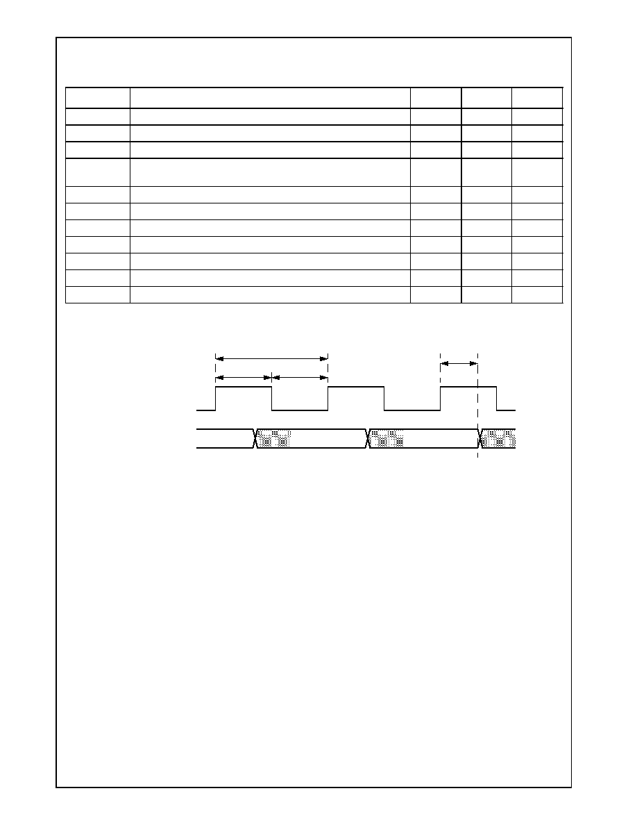
Revision 3.1
191
www.national.com
Electrical Specifications (
Continued
)
GeodeTM
G
Xm
P
r
ocessor
Table 7-11. Video Interface Signals
Figure 7-8. Graphics Port Timing
Symbol
Parameter
Min
Max
Unit
t1
PCLK Period
7.4
40
ns
t2
PCLK High Time
3
ns
t3
PCLK Low Time
3
ns
t4
PIXEL[17:0], CRT_HSYNC, CRT_VSYNC, FP_HSYNC,
FP_VSYNC, ENA_DISP Valid Delay from PCLK Rising Edge
2
5
ns
t5
VID_CLK Period
8.5
ns
t6
VID_RDY Setup to VID_CLK Rising Edge
5
ns
t7
VID_RDY Hold to VID_CLK Rising Edge
2
ns
t8
VID_VAL, VID_DATA[7:0] Valid Delay from VID_CLK Rising Edge
2
5
ns
t9
DCLK Period
7.4
ns
t10
DCLK Rise/Fall Time
3
ns
tcyc
DCLK Duty Cycle
40
60
%
t1
t2
t3
t4
PCLK
PIXEL[17:0],
CRT_HSYNC, CRT_VSYNC,
FP_HSYNC, FP_VSYNC,
ENA_DISP

www.national.com
192
Revision 3.1
Electrical Specifications (
Continued
)
GeodeTM
G
Xm
Pr
ocessor
Figure 7-9. Video Port Timing
Figure 7-10. DCLK Timing
t5
t8
VID_VAL
VID_CLK
VID_DATA[7:0]
t6
t7
VID_RDY
DCLK
t10
t9

Revision 3.1
193
www.national.com
Electrical Specifications (
Continued
)
GeodeTM
G
Xm
P
r
ocessor
Table 7-12. JTAG AC Specification
Figure 7-11. TCK Timing and Measurement Points
Symbol
Parameter
Min
Max
Unit
TCK Frequency (MHz)
25
MHz
t1
TCK Period
40
ns
t2
TCK High Time
10
ns
t3
TCK Low Time
10
ns
t4
TCK Rise Time
4
ns
t5
TCK Fall Time
4
ns
t6
TDO Valid Delay
3
25
ns
t7
Non-test Outputs Valid Delay
3
25
ns
t8
TDO Float Delay
30
ns
t9
Non-test Outputs Float Delay
36
ns
t10
TDI, TMS Setup Time
8
ns
t11
Non-test Inputs Setup Time
8
ns
t12
TDI, TMS Hold Time
7
ns
t13
Non-test Inputs Hold Time
7
ns
TCK
1.5 V
V
IH(Min)
V
IL(Max)
t2
t1
t4
t5
t3

www.national.com
194
Revision 3.1
Electrical Specifications (
Continued
)
GeodeTM
G
Xm
Pr
ocessor
Figure 7-12. JTAG Test Timings
TCK
TDI,
TMS
1.5 V
t10
t8
t12
t6
t7
t9
t11
t13
TDO
Output
Signals
Input
Signals

Revision 3.1
195
www.national.com
GeodeTM
G
Xm
P
r
ocessor
8.0
Package Specifications
The thermal characteristics and mechanical dimensions
for the Geode GXm processor are provided on the follow-
ing pages.
8.1 THERMAL CHARACTERISTICS
Table 8-1 shows the junction-to-case thermal resistance
of the SPGA and BGA package and can be used to calcu-
late the junction (die) temperature under any given cir-
cumstance.
Note that there is no specification for maximum junction
temperature given since the operation of both SPGA and
BGA devices are guaranteed to a case temperature range
of 0∞C to 85∞C. As long as the case temperature of the
device is maintained within this range, the junction tem-
perature of the die will also be maintained within its allow-
able
operating
range.
However,
the
die
(junction)
temperature under a given operating condition can be cal-
culated by using the following equation:
T
J
= T
C
+ (P *
JC
)
where:
T
J
= Junction temperature (∞C)
T
C
= Case temperature at top center of package (∞C)
P = Power dissipation (W)
J
C = Junction-to-case thermal resistance (∞C/W)
As stated previously, a maximum junction temperature is
not specified since a maximum case temperature is.
Therefore, the following equation can be used to calculate
the maximum thermal resistance required of the thermal
solution for a given maximum ambient temperature:
where:
CS
= Max case-to-heatsink thermal resistance
(∞C/W) allowed for thermal solution.
SA
= Max heatsink-to-ambient thermal resistance
(∞C/W) allowed for thermal solution.
T
A
= Max ambient temperature (∞C)
T
C
= Max case temperature at top center of package
(∞C)
P = Max power dissipation (W)
If thermal grease is used between the case and heatsink,
CS
will reduce to about 0.01 ∞C/W. Therefore, the above
equation can be simplified to:
where:
CA
=
CS
= Max case-to-ambient thermal resistance
(∞C/W) allowed for thermal solution.
The calculated
CA
value (examples shown in Table 8-2)
represents the maximum allowed thermal resistance of
the selected cooling solution which is required to maintain
the 85∞C case temperature for the application in which the
device is used.
These examples are given for reference only. The actual
value used for Maximum Power (P) and ambient tempera-
ture (T
A
) is determined by the system designer based on
system configuration, extremes of the operating environ-
ment, and whether active thermal management (via Sus-
pend Modulation) of the processor is employed.
Table 8-1. Junction-to-Case Thermal Resistance
for SPGA and BGA Packages
Package
J
C
SPGA
1.7
∞
C/W
BGA
1.1
∞
C/W
C
S
S
A
+
T
C
T
A
≠
P
----------------------
=
CA
T
C
T
A
≠
P
----------------------
=

www.national.com
196
Revision 3.1
Package Specifications (
Continued
)
GeodeTM
G
Xm
Pr
ocessor
8.1.1
Heatsink Considerations
As described previously, Table 8-2 shows the maximum
allowed thermal resistance of a heatsink for particular
operating environments. The calculated values, defined
as
CA
, represent the required ability of a particular heat-
sink to transfer heat generated by the processor from its
case into the air, thereby maintaining the case tempera-
ture at or below 85∞C. Because
CA
is a measure of ther-
mal resistivity, it is inversely proportional to the heatsink's
ability to dissipate heat or it's thermal conductivity.
Note:
A "perfect" heatsink would be able to maintain a
case temperature equal to that of the ambient air
inside the system chassis.
Looking at Table 8-2, it can be seen that as ambient tem-
perature (T
A
) increases,
CA
decreases, and that as power
consumption
of
the
processor
(P)
increases,
CA
decreases. Thus, the ability of the heatsink to dissipate
thermal energy must increase as the processor power
increases and as the temperature inside the enclosure
increases.
While
CA
is a useful parameter to calculate, heatsinks are
not typically specified in terms of a single
CA
. This is
because the thermal resistivity of a heatsink is not con-
stant across power or temperature. In fact, heatsinks
become slightly less efficient as the amount of heat they
are trying to dissipate increases. For this reason, heatsinks
are typically specified by graphs that plot heat dissipation
(in watts) vs. mounting surface (case) temperature rise
above ambient (in ∞C). This method is necessary because
ambient and case temperatures fluctuate constantly dur-
ing normal operation of the system. The system designer
must be careful to choose the proper heatsink by match-
ing the required
CA
with the thermal dissipation curve of
the device under the entire range of operating conditions in
order to make sure that a case temperature of 85∞C is
never surpassed.
Table 8-2. Case-to-Ambient Thermal Resistance Examples @ 85∞C
Core Voltage
(V
CC2
)
Core
Frequency
Maximum
Power
CA
for Different Ambient Temperatures (∞C/W)
20∞C
25∞C
30∞C
35∞C
40∞C
2.9V
(Nominal)
266 MHz
7.7W
8.44
7.79
7.14
6.49
5.84
233 MHz
7.1W
9.15
8.45
7.75
7.04
6.34
200 MHz
6.4W
10.16
9.38
8.59
7.81
7.03
180 MHz
6.0W
10.83
10.00
9.17
8.33
7.50

Revision 3.1
197
www.national.com
Package Specifications (
Continued
)
GeodeTM
G
Xm
P
r
ocessor
To choose the proper heatsink, the system designer must
make sure that the calculated
CA
falls above the curve
(shaded area). The curve itself defines the minimum tem-
perature rise above ambient that the heatsink can main-
tain.
See Figure 8-1 as an example of a particular heatsink
under consideration.
Figure 8-1. Heatsink Example
Example 1
Assume P (max) = 5W and T
A
(max) = 40∞C.
Therefore:
In this case, the heatsink under consideration is more than
adequate since at 5W worst case, it can maintain a 40∞C
case temperature rise above ambient (
CA
= 9) when a
maximum of 45∞C (
CA
= 8) is required.
Example 2
Assume P (max) = 10W and T
A
(max) = 40∞C.
Therefore:
In this case, the heatsink under consideration is NOT ade-
quate to maintain the 45∞C case temperature rise above
ambient for a 9W processor.
For more information on thermal design considerations or
heatsink properties, refer to the Product Selection Guide of
any leading vendor of Thermal Engineering solutions.
0
10
20
30
40
50
2
4
6
8
10
CA = 45/9 = 5
Heat Dissipated - Watts
CA = 45/5 = 9
M
ount
ing
S
urf
a
ce
T
e
mperat
ure
Rise
A
bo
v
e
Am
bi
e
n
t
≠
∞C
CA
T
C
T
A
≠
P
----------------------
=
CA
85
40
≠
(
)
5
----------------------
=
CA
9
=
CA
T
C
T
A
≠
P
----------------------
=
CA
85
40
≠
(
)
9
----------------------
=
CA
5
=
www.national.com
198
Revision 3.1
Package Specifications (
Continued
)
GeodeTM
G
Xm
Pr
ocessor
8.2
MECHANICAL PACKAGE OUTLINES
Dimensions for the BGA package are shown in Figure 8-2. Figure 8-3 shows the SPGA dimensions. Table 8-3 gives the
legend for the symbols used in both package outlines.
Figure 8-2. 352-Terminal BGA Mechanical Package Outline
Sym
Millimeters
Inches
Min
Max
Min
Max
A
1.45
2.23
0.057
0.088
A1
0.50
0.70
0.020
0.028
A2
0.43
0.83
0.017
0.033
aaa
0.20
0.008
B
0.60
0.90
0.024
0.035
D
34.80
35.20
1.370
1.386
D1
31.55
31.95
1.242
1.258
D2
32.80
35.20
1.291
1.386
E1
1.12
1.42
0.044
0.056
F
0.35
0.014
S1
1.42
1.82
0.056
0.072
F
D2
A01 Index Chamfer
1.5 mm on a side
45 Degree Angle
CU Heat
Spreader
.889
REF.
S1
D1
D
D
1.5
1.5
E1
B
A1
A2
A
Seating
Plane
aaa Z
Z
Revision 3.1
199
www.national.com
Package Specifications (
Continued
)
GeodeTM
G
Xm
P
r
ocessor
Figure 8-3. 320-Pin SPGA Mechanical Package Outline
F
D
A01 index mark
.030" blank circle
inside .060" filled
circle to form donut
45 CHAMFER
Pin C3
2.29
1.52
REF.
(INDEX CORNER)
1.65
REF.
S1
D1
D
D
o
Sym
Millimeters
Inches
Min
Max
Min
Max
A
2.51
3.07
0.099
0.121
B
0.43
0.51
0.017
0.020
D
49.28
49.91
1.940
1.965
D1
45.47
45.97
1.790
1.810
E1
2.41
2.67
0.095
0.105
E2
1.14
1.40
0.045
0.055
F
--
0.127
Diag
--
0.005
Diag
L
2.97
3.38
0.117
0.133
S1
1.65
2.16
0.065
0.085
SEATING
PLANE
L
E2
E1
B
A
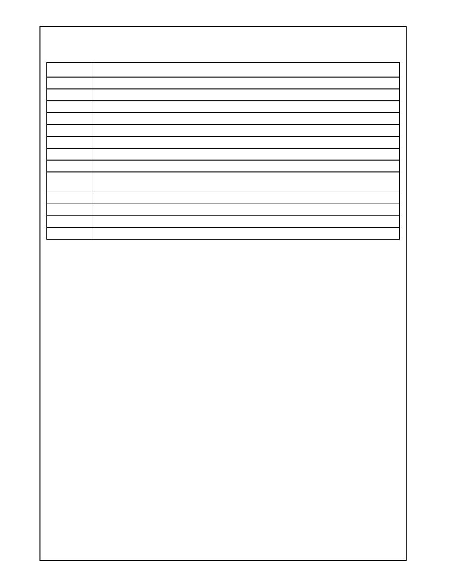
www.national.com
200
Revision 3.1
Package Specifications (
Continued
)
GeodeTM
G
Xm
Pr
ocessor
Table 8-3. Mechanical Package Outline Legend
Symbol
Meaning
A
Distance from seating plane datum to highest point of body
A1
Solder ball height
A2
Laminate thickness (excluding heat spreader)
aaa
Coplanarity
B
Pin or solder ball diameter
D
Largest overall package outline dimension
D1
Length from outer pin center to outer pin center
D2
Heat spreader outline dimension
E1
BGA: Solder ball pitch
SPGA: Linear spacing between true pin position centerlines
E2
Diagonal spacing between true pin position centerlines
F
Flatness
L
Distance from seating plane to tip of pin
S1
Length from outer pin/ball center to edge of laminate

Revision 3.1
201
www.national.com
GeodeTM
G
Xm
P
r
ocessor
9.0
Instruction Set
This section summarizes the Geode GXm processor
instruction set and provides detailed information on the
instruction encodings. The instruction set is broken into
four categories:
∑ Processor Core Instruction Set - listed in Table 9-27 on
page 213
∑ FPU Instruction Set - listed in Table 9-29 on page 225
∑ MMX Instruction Set - listed in Table 9-31 on page 230
∑ National Semiconductor Extended MMX Instruction Set
- listed in Table 9-33 on page 235
These tables provide information on the instruction encod-
ing, and the instruction clock counts for each instruction.
The clock count values for these tables are based on the
following assumptions
1.
All clock counts refer to the microprocessor core
internal clock frequency. For example, clock doubled
GXm
processor
cores
will
reference
a
clock
frequency that is twice the bus frequency.
2.
The instruction has been prefetched, decoded and is
ready for execution.
3.
Bus cycles do not require wait states.
4.
There are no local bus HOLD requests delaying
processor access to the bus.
5.
No exceptions are detected during instruction execu-
tion.
6.
If an effective address is calculated, it does not use
two general register components. One register,
scaling and displacement can be used within the
clock count shown. However, if the effective address
calculation uses two general register components,
add one clock to the clock count shown.
7.
All clock counts assume aligned 32-bit memory/ IO
operands.
8.
If instructions access a 32-bit operand on odd
addresses, add one clock for read or write and add
two clocks for read and write.
9.
For non-cached memory accesses, add two clocks
(clock doubled GXm processor cores) or four clocks
(clock tripled GXm processor cores), assuming zero
wait state memory accesses.
10. Locked cycles are not cacheable. Therefore, using the
LOCK prefix with an instruction adds additional clocks
as specified in item 9 above.
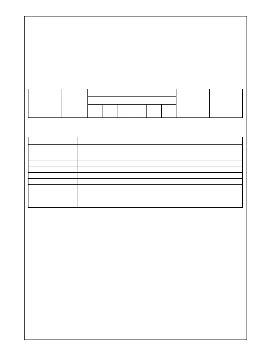
www.national.com
202
Revision 3.1
Instruction Set (
Continued
)
GeodeTM
G
Xm
Pr
ocessor
9.1
GENERAL INSTRUCTION SET FORMAT
Depending on the instruction, the GXm processor core
instructions follow the general instruction format shown in
Table 9-1.
These instructions vary in length and can start at any byte
address. An instruction consists of one or more bytes that
can include prefix bytes, at least one opcode byte, a mod
r/m byte, an s-i-b byte, address displacement, and imme-
diate data. An instruction can be as short as one byte and
as long as 15 bytes. If there are more than 15 bytes in the
instruction, a general protection fault (error code 0) is gen-
erated.
The fields in the general instruction format at the byte
level are summarized in Table 9-2 and detailed in the fol-
lowing subsections.
Table 9-1. General Instruction Set Format
Prefix (optional)
Opcode
Register and Address Mode Specifier
Address
Displacement
Immediate
Data
mod r/m Byte
s-i-b Byte
mod
reg
r/m
ss
index
base
0 or More Bytes
1 or 2 Bytes
7:6
5:3
2:0
7:6
5:3
2:0
0, 8, 16, or 32 Bits
0, 8, 16, or 32 Bits
Table 9-2. Instruction Fields
Field Name
Description
Prefix (optional)
Prefix Field(s): One or more optional fields that are used to specify segment register override, address
and operand size, repeat elements in string instruction, LOCK# assertion.
Opcode
Opcode Field: Identifies instruction operation.
mod
Address Mode Specifier: Used with r/m field to select addressing mode.
reg
General Register Specifier: Uses reg, sreg3 or sreg2 encoding depending on opcode field.
r/m
Address Mode Specifier: Used with mod field to select addressing mode.
ss
Scale factor: Determines scaled-index address mode.
index
Index: Determines general register to be used as index register.
base
Base: Determines general register to be used as base register.
Address Displacement
Displacement: Determines address displacement.
Immediate Data
Immediate Data: Immediate-data operand used by instruction.
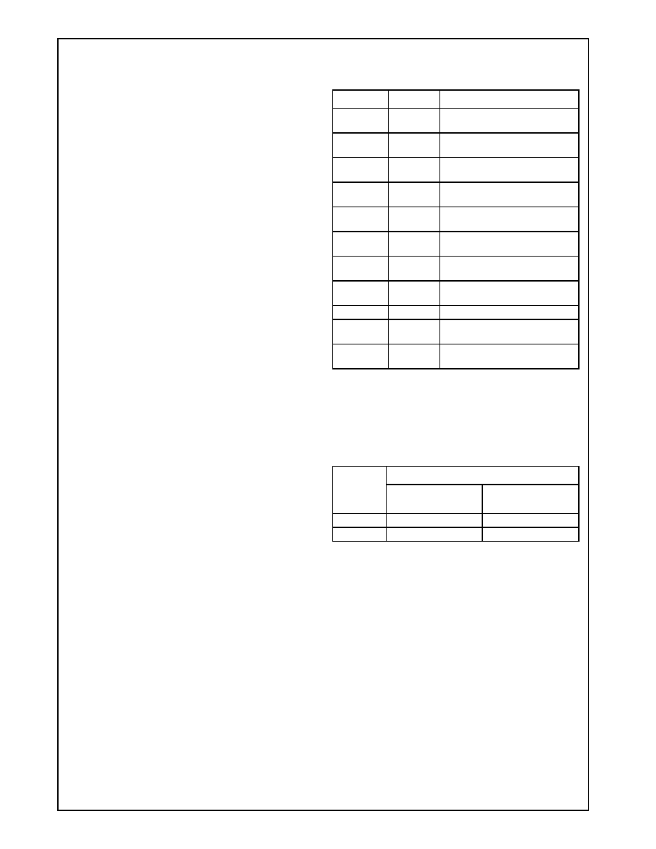
Revision 3.1
203
www.national.com
Instruction Set (
Continued
)
GeodeTM
G
Xm
P
r
ocessor
9.1.1
Prefix (Optional)
Prefix bytes can be placed in front of any instruction to
modify the operation of that instruction. When more than
one prefix is used, the order is not important. There are
five types of prefixes that can be used:
1.
Segment Override explicitly specifies which segment
register the instruction will use for effective address
calculation.
2.
Address Size switches between 16-bit and 32-bit
addressing by selecting the non-default address size.
3.
Operand Size switches between 16-bit and 32-bit
operand size by selecting the non-default operand
size.
4.
Repeat is used with a string instruction to cause the
instruction to be repeated for each element of the
string.
5.
Lock is used to assert the hardware LOCK# signal
during execution of the instruction.
Table 9-3 lists the encoding for different types of prefix
bytes.
9.1.2
Opcode
The opcode field specifies the operation to be performed
by the instruction. The opcode field is either one or two
bytes in length and may be further defined by additional
bits in the mod r/m byte. Some operations have more than
one opcode, each specifying a different form of the opera-
tion. Certain opcodes name instruction groups. For exam-
ple, opcode 80h names a group of operations that have
an immediate operand and a register or memory operand.
The reg field may appear in the second opcode byte or in
the mod r/m byte.
The opcode may contain w, d, s and eee opcode fields as
shown in the Table 9-27 on page 213
9.1.2.1
w Field (Operand Size)
When used, the 1-bit w field selects the operand size dur-
ing 16-bit and 32-bit data operations. See Table 9-4.
Table 9-3. Instruction Prefix Summary
Prefix
Encoding
Description
ES:
26h
Override segment default, use ES
for memory operand.
CS:
2Eh
Override segment default, use CS
for memory operand.
SS:
36h
Override segment default, use SS
for memory operand.
DS:
3Eh
Override segment default, use DS
for memory operand.
FS:
64h
Override segment default, use FS
for memory operand.
GS:
65h
Override segment default, use GS
for memory operand.
Operand
Size
66h
Make operand size attribute the
inverse of the default.
Address
Size
67h
Make address size attribute the
inverse of the default.
LOCK
F0h
Assert LOCK# hardware signal.
REPNE
F2h
Repeat the following string
instruction.
REP/REPE
F3h
Repeat the following string
instruction.
Table 9-4. w Field Encoding
w
Field
Operand Size
16-Bit Data
Operations
32-Bit Data
Operations
0
8 bits
8 bits
1
16 bits
32 bits

www.national.com
204
Revision 3.1
Instruction Set (
Continued
)
GeodeTM
G
Xm
Pr
ocessor
9.1.2.2
d Field (Operand Direction)
When used, the d field (bit 1) determines which operand is
taken as the source operand and which operand is taken
as the destination. See Table 9-5.
9.1.2.3
s Field (Immediate Data Field Size)
When used, the s field (bit 1) determines the size of the
immediate data field. If the s bit is set, the immediate field
of the opcode is 8 bits wide and is sign-extended to match
the operand size of the opcode. See Table 9-6.
9.1.2.4
eee Field (MOV-Instruction Register
Selection)
The eee field (bits [5:3]) is used to select the control,
debug and test registers in the MOV instructions. The type
of register and base registers selected by the eee field are
listed in Table 9-7. The values shown in Table 9-7 are the
only valid encodings for the eee bits.
Table 9-5. d Field Encoding
d
Field
Direction of
Operation
Source
Operand
Destination
Operand
0
Register-to-Register
or
Register-to-Memory
reg
mod r/m
or
mod ss-index-
base
1
Register-to-Register
or
Memory-to-Register
mod r/m
or
mod ss-index-
base
reg
Table 9-6. s Field Encoding
s
Field
Immediate Field Size
8-Bit
Operand Size
16-Bit
Operand Size
32-Bit
Operand Size
0 (or not
present)
8 bits
16 bits
32 bits
1
8 bits
8 bits
(sign-extended)
8 bits
(sign-extended)
Table 9-7. eee Field Encoding
eee Field
Register Type
Base Register
000
Control Register
CR0
010
Control Register
CR2
011
Control Register
CR3
100
Control Register
CR4
000
Debug Register
DR0
001
Debug Register
DR1
010
Debug Register
DR2
011
Debug Register
DR3
110
Debug Register
DR6
111
Debug Register
DR7
011
Test Register
TR3
100
Test Register
TR4
101
Test Register
TR5
110
Test Register
TR6
111
Test Register
TR7
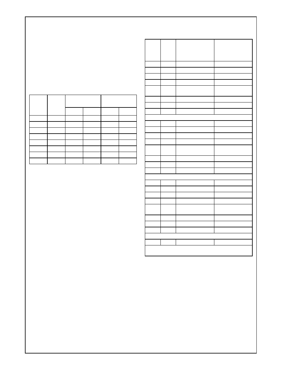
Revision 3.1
205
www.national.com
Instruction Set (
Continued
)
GeodeTM
G
Xm
P
r
ocessor
9.1.3
mod and r/m Byte (Memory Addressing)
The mod and r/m fields within the mod r/m byte, select the
type of memory addressing to be used. Some instructions
use a fixed addressing mode (e.g., PUSH or POP) and
therefore, these fields are not present. Table 9-8 lists the
addressing method when 16-bit addressing is used and a
mod r/m byte is present. Some mod r/m field encodings
are dependent on the w field and are shown in Table 9-8.
Table 9-8. General Registers Selected by mod
r/m Fields and w Field
mod
r/m
16-Bit
Operation
32-Bit
Operation
w = 0
w = 1
w = 0
w = 1
11
000
AL
AX
AL
EAX
11
001
CL
CX
CL
ECX
11
010
DL
DX
DL
EDX
11
011
BL
BX
BL
EBX
11
100
AH
SP
AH
ESP
11
101
CH
BP
CH
EBP
11
110
DH
SI
DH
ESI
11
111
BH
DI
BH
EDI
Table 9-9. mod r/m Field Encoding
mod
Field
r/m
Field
16-Bit Address
Mode with
mod r/m Byte
32-Bit Address
Mode with mod r/m
Byte and No s-i-b
Byte Present
00
000
DS:[BX+SI]
DS:[EAX]
00
001
DS:[BX+DI]
DS:[ECX]
00
010
SS:[BP+SI]
DS:[EDX]
00
011
SS:[BP+DI]
DS:[EBX]
00
100
DS:[SI]
s-i-b is present
(See Table 9-15)
00
101
DS:[DI]
DS:[d32]
00
110
DS:[d16]
DS:[ESI]
00
111
DS:[BX]
DS:[EDI]
01
000
DS:[BX+SI+d8]
DS:[EAX+d8]
01
001
DS:[BX+DI+d8]
DS:[ECX+d8]
01
010
SS:[BP+SI+d8]
DS:[EDX+d8]
01
011
SS:[BP+DI+d8]
DS:[EBX+d8]
01
100
DS:[SI+d8]
s-i-b is present
(See Table 9-15)
01
101
DS:[DI+d8]
SS:[EBP+d8]
01
110
SS:[BP+d8]
DS:[ESI+d8]
01
111
DS:[BX+d8]
DS:[EDI+d8]
10
000
DS:[BX+SI+d16]
DS:[EAX+d32]
10
001
DS:[BX+DI+d16]
DS:[ECX+d32]
10
010
SS:[BP+SI+d16]
DS:[EDX+d32]
10
011
SS:[BP+DI+d16]
DS:[EBX+d32]
10
100
DS:[SI+d16]
s-i-b is present
(See Table 9-15)
10
101
DS:[DI+d16]
SS:[EBP+d32]
10
110
SS:[BP+d16]
DS:[ESI+d32]
10
111
DS:[BX+d16]
DS:[EDI+d32]
11
xxx
See Table 9-8.
See Table 9-8
Note: Note: d8 refers to 8-bit displacement, and d16 refers to
16-bit displacement.
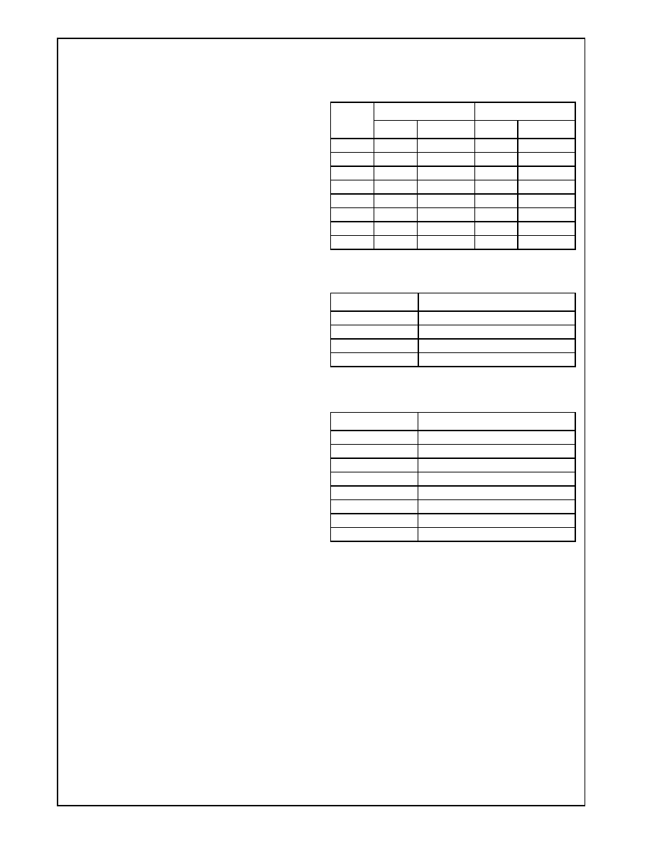
www.national.com
206
Revision 3.1
Instruction Set (
Continued
)
GeodeTM
G
Xm
Pr
ocessor
9.1.4
reg Field
The reg field (Table 9-10) determines which general regis-
ters are to be used. The selected register is dependent on
whether a 16- or 32-bit operation is current and on the sta-
tus of the w bit.
9.1.4.1
sreg2 Field (ES, CS, SS, DS Register
Selection)
The sreg2 field (Table 9-11) is a 2-bit field that allows one
of the four 286-type segment registers to be specified.
9.1.4.2
sreg3 Field (FS and GS Segment Register
Selection)
The sreg3 field (Table 9-12) is 3-bit field that is similar to
the sreg2 field, but allows use of the FS and GS segment
registers.
Table 9-10. General Registers Selected
by reg Field
reg
16-Bit Operation
32-Bit Operation
w = 0
w = 1
w = 0
w = 1
000
AL
AX
AL
EAX
001
CL
CX
CL
ECX
010
DL
DX
DL
EDX
011
BL
BX
BL
EBX
100
AH
SP
AH
ESP
101
CH
BP
CH
EBP
110
DH
SI
DH
ESI
111
BH
DI
BH
EDI
Table 9-11. sreg2 Field Encoding
sreg2 Field
Segment Register Selected
00
ES
01
CS
10
SS
11
DS
Table 9-12. sreg3 Field Encoding
sreg3 Field
Segment Register Selected
000
ES
001
CS
010
SS
011
DS
100
FS
101
GS
110
Undefined
111
Undefined
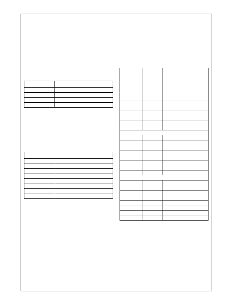
Revision 3.1
207
www.national.com
Instruction Set (
Continued
)
GeodeTM
G
Xm
P
r
ocessor
9.1.5
s-i-b Byte (Scale, Indexing, Base)
The s-i-b fields provide scale factor, indexing and a base
field for address selection. The ss, index and base fields
are described next.
9.1.5.1
ss Field (Scale Selection)
The ss field (Table 9-13) specifies the scale factor used in
the offset mechanism for address calculation. The scale
factor multiplies the index value to provide one of the com-
ponents used to calculate the offset address.
9.1.5.2
index Field (Index Selection)
The index field (Table 9-14) specifies the index register
used by the offset mechanism for offset address calcula-
tion. When no index register is used (index field = 100),
the ss value must be 00 or the effective address is unde-
fined.
9.1.5.3
Base Field (s-i-b Present)
In Table 9-9 on page 205, the note "s-i-b present" for cer-
tain entries forces the use of the mod and base field as
listed in Table 9-15. The first two digits in the first column
of Table 9-15 identify the mod bits in the mod r/m byte.
The last three digits in the first column of this table identi-
fies the base fields in the s-i-b byte.
Table 9-13. ss Field Encoding
ss Field
Scale Factor
00
x1
01
x2
01
x4
11
x8
Table 9-14. index Field Encoding
Index Field
Index Register
000
EAX
001
ECX
010
EDX
011
EBX
100
none
101
EBP
110
ESI
111
EDI
Table 9-15. mod base Field Encoding
mod Field
within
mode/rm
Byte
(bits 7:6)
base Field
within
s-i-b
Byte
(bits 2:0)
32-Bit Address Mode
with mod r/m and s-i-b
Bytes Present
00
000
DS:[EAX+(scaled index)]
00
001
DS:[ECX+(scaled index)]
00
010
DS:[EDX+(scaled index)]
00
011
DS:[EBX+(scaled index)]
00
100
SS:[ESP+(scaled index)]
00
101
DS:[d32+(scaled index)]
00
110
DS:[ESI+(scaled index)]
00
111
DS:[EDI+(scaled index)]
01
000
DS:[EAX+(scaled index)+d8]
01
001
DS:[ECX+(scaled index)+d8]
01
010
DS:[EDX+(scaled index)+d8]
01
011
DS:[EBX+(scaled index)+d8]
01
100
SS:[ESP+(scaled index)+d8]
01
101
SS:[EBP+(scaled index)+d8]
01
110
DS:[ESI+(scaled index)+d8]
01
111
DS:[EDI+(scaled index)+d8]
10
000
DS:[EAX+(scaled index)+d32]
10
001
DS:[ECX+(scaled index)+d32]
10
010
DS:[EDX+(scaled index)+d32]
10
011
DS:[EBX+(scaled index)+d32]
10
100
SS:[ESP+(scaled index)+d32]
10
101
SS:[EBP+(scaled index)+d32]
10
110
DS:[ESI+(scaled index)+d32]
10
111
DS:[EDI+(scaled index)+d32]
www.national.com
208
Revision 3.1
Instruction Set (
Continued
)
GeodeTM
G
Xm
Pr
ocessor
9.2
CPUID INSTRUCTION
The CPUID instruction (opcode 0FA2) allows the software
to make processor inquiries as to the vendor, family,
model, stepping, features and also provides cache infor-
mation. The GXm with MMX supports both the standard
and National Semiconductor extended CPUID levels.
The presence of the CPUID instruction is indicated by the
ability to change the value of the ID Flag, bit 21 in the
EFLAGS register.
The CPUID level allows the CPUID instruction to return
different information in the EAX, EBX, ECX, and EDX reg-
isters. The level is determined by the initialized value of
the EAX register before the instruction is executed. A
summary of the CPUID levels is shown in Table 9-16.
9.2.1
Standard CPUID Levels
The standard CPUID levels are part of the standard x86
instruction set.
9.2.1.1
CPUID Instruction with EAX = 00000000h
Standard function 0h (EAX = 0) of the CPUID instruction
returns the maximum standard CPUID levels as well as
the processor vendor string.
After the instruction is executed, the EAX register contains
the maximum standard CPUID levels supported. The
maximum standard CPUID level is the highest acceptable
value for the EAX register input. This does not include the
extended CPUID levels.
The EBX through EDX registers contain the vendor string
of the processor as shown in Table 9-17.
9.2.1.2
CPUID Instruction with EAX = 00000001h
Standard function 01h (EAX = 1) of the CPUID instruction
returns the processor type, family, model, and stepping
information of the current processor in the EAX register
(see Table 9-18). The EBX and ECX registers are
reserved.
The standard feature flags supported are returned in the
EDX register as shown in Table 9-19 on page 209. Each
flag refers to a specific feature and indicates if that feature
is present on the processor. Some of these features have
protection control in CR4. Before using any of these fea-
tures on the processor, the software should check the cor-
responding feature flag. Attempting to execute an
unavailable feature can cause exceptions and unexpected
behavior. For example, software must check bit 4 before
attempting to use the Time Stamp Counter instruction.
Table 9-16. CPUID Levels Summary
CPUID
Type
Initialized
EAX
Register
Returned Data in EAX, EBX,
ECX, EDX Registers
Standard
00000000h
Maximum standard levels, CPU
vendor string
Standard
00000001h
Model, family, type and features
Standard
00000002h
TLB and cache information
Extended
80000000h
Maximum extended levels
Extended
80000001h
Extended model, family, type and
features
Extended
80000002h
CPU marketing name string
Extended
80000003h
Extended
80000004h
Extended
80000005h
TLB and L1 cache description
Table 9-17. CPUID Data Returned when EAX = 0
Register
(Note)
Returned Contents
Description
EAX
2
Maximum Standard
Level
EBX
69
72
7943
(iryC)
Vendor ID String 1
EDX
73
6E
4978
(snlx)
Vendor ID String 2
ECX
64
61
6574
(daet)
Vendor ID String 3
Note: The register column is intentionally out of order.
Table 9-18. EAX, EBX, ECX CPUID Data
Returned when EAX = 1
Register
Returned
Contents
Description
EAX[3:0]
xx
Stepping ID
EAX[7:4]
4
Model
EAX[11:8]
5
Family
EAX[15:12]
0
Type
EAX[31:16]
-
Reserved
EBX
-
Reserved
ECX
-
Reserved
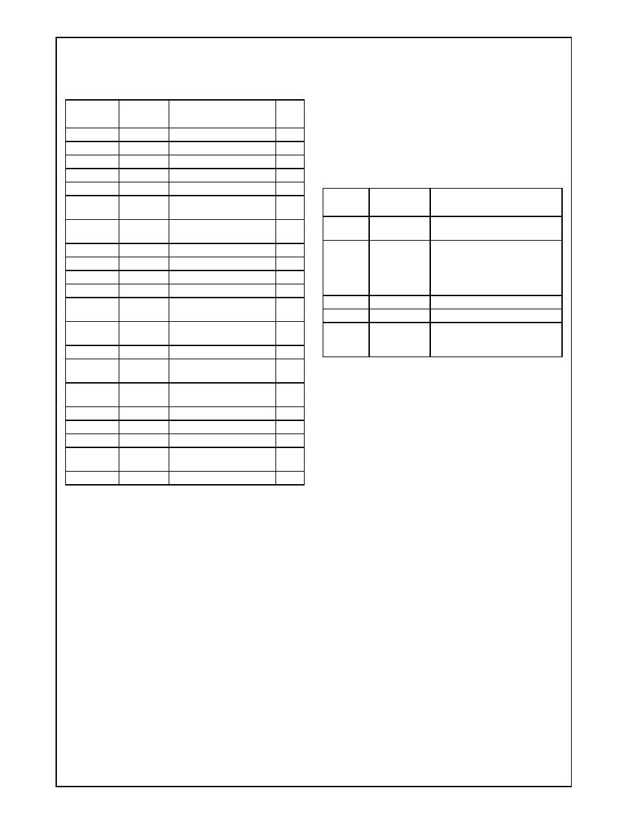
Revision 3.1
209
www.national.com
Instruction Set (
Continued
)
GeodeTM
G
Xm
P
r
ocessor
9.2.1.3
CPUID Instruction with EAX = 00000002h
Standard function 02h (EAX = 02h) of the CPUID instruc-
tion returns information that is specific to the National
Semiconductor family of processors. Information about
the TLB is returned in EAX as shown in Table 9-20. Infor-
mation about the L1 cache is returned in EDX.
Table 9-19. EDX CPUID Data
Returned when EAX = 1
EDX
Returned
Contents*
Feature Flag
CR4
Bit
EDX[0]
1
FPU On-Chip
-
EDX[1]
0
Virtual Mode Extension
-
EDX[2]
0
Debug Extensions
-
EDX[3]
0
Page Size Extensions
-
EDX[4]
1
Time Stamp Counter
2
EDX[5]
1
RDMSR / WRMSR
Instructions
-
EDX[6]
0
Physical Address
Extensions
-
EDX[7]
0
Machine Check Exception
-
EDX[8]
1
CMPXCHG8B Instruction
-
EDX[9]
0
On-Chip APIC Hardware
-
EDX[10]
0
Reserved
-
EDX[11]
0
SYSENTER / SYSEXIT
Instructions
-
EDX[12]
0
Memory Type Range
Registers
-
EDX[13]
0
Page Global Enable
-
EDX[14]
0
Machine Check
Architecture
-
EDX[15]
1
Conditional Move
Instructions
-
EDX[16]
0
Page Attribute Table
-
EDX[22:17]
0
Reserved
-
EDX[23]
1
MMX Instructions
-
EDX[24]
0
Fast FPU Save and
Restore
-
EDX[31:25]
0
Reserved
-
Note: *0 = Not supported
Table 9-20. Standard CPUID with
EAX = 00000002h
Register
Returned
Contents
Description
EAX
xx xx 70 xxh
TLB is 32 Entry, 4-way set asso-
ciative, and has 4 KByte Pages
EAX
xx xx xx 01h
The CPUID instruction needs to
be executed only once with an
input value of 02h to retrieve
complete information about the
cache and TLB
EBX
Reserved
ECX
Reserved
EDX
xx xx xx 80h
L1 cache is 16 KBytes, 4-way set
associated, and has 16 bytes per
line.

www.national.com
210
Revision 3.1
Instruction Set (
Continued
)
GeodeTM
G
Xm
Pr
ocessor
9.2.2
Extended CPUID Levels
Testing for extended CPUID instruction support can be
accomplished by executing a CPUID instruction with the
EAX register initialized to 80000000h. If a value greater
than or equal to 80000000h is returned to the EAX regis-
ter by the CPUID instruction, the processor supports
extended CPUID levels.
9.2.2.1
CPUID Instruction with
EAX = 8000000h
Extended function 80000000h (EAX = 80000000h) of the
CPUID instruction returns the maximum extended CPUID
levels supported by the current processor in EAX (Table 9-
21). The EBX, ECX, and EDX registers are currently
reserved.
9.2.2.2
CPUID Instruction with
EAX = 8000 0001h
Extended function 80000001h (EAX = 80000001h) of the
CPUID instruction returns the processor type, family,
model, and stepping information of the current processor
in EAX. The EBX and ECX registers are reserved.
The extended feature flags supported are returned in the
EDX register as shown in Table 9-23. Each flag refers to a
specific feature and indicates if that feature is present on
the processor. Some of these features have protection
control in CR4. Before using any of these features on the
processor, the software should check the corresponding
feature flag.
Table 9-21. Maximum Extended CPUID Level
Register
Returned
Contents
Description
EAX
80000005h
Maximum Extended CPUID
Level (six levels)
EBX
-
Reserved
ECX
-
Reserved
EDX
-
Reserved
Table 9-22. EAX, EBX, ECX CPUID Data
Returned when EAX = 80000001h
Register
Returned
Contents
Description
EAX[3:0]
xx
Stepping ID
EAX[7:4]
4
Model
EAX[11:8]
5
Family
EAX[15:12]
0
Processor Type
EAX[31:16]
-
Reserved
EBX
-
Reserved
ECX
-
Reserved
Table 9-23. EDX CPUID Data Returned
when EAX = 80000001h
EDX
Returned
Contents*
Feature Flag
CR4
Bit
EDX[0]
1
FPU On-Chip
-
EDX[1]
0
Virtual Mode Extension
-
EDX[2]
0
Debugging Extension
-
EDX[3]
0
Page Size Extension
(4 MB)
-
EDX[4]
1
Time Stamp Counter
2
EDX[5]
1
National Semiconductor
Model-Specific Registers
(via RDMSR / WRMSR
Instructions)
-
EDX[6]
0
Reserved
-
EDX[7]
0
Machine Check Exception
-
EDX[8]
1
CMPXCHG8B Instruction
-
EDX[9]
0
Reserved
-
EDX[10]
0
Reserved
-
EDX[11]
0
SYSCALL / SYSRET
Instruction
-
EDX[12]
0
Reserved
-
EDX[13]
0
Page Global Enable
-
EDX[14]
0
Reserved
-
EDX[15]
1
Integer Conditional Move
Instruction
-
EDX[16]
0
FPU Conditional Move
Instruction
-
EDX[22:17]
0
Reserved
-
EDX[23]
1
MMX
-
EDX[24]
1
6x86MX Multimedia
Extensions
-
Note: 0 = Not supported

Revision 3.1
211
www.national.com
Instruction Set (
Continued
)
GeodeTM
G
Xm
P
r
ocessor
9.2.2.3
CPUID Instruction with
EAX = 80000002h, 80000003h, 80000004h
Extended functions 80000002h through 80000004h (EAX
= 80000002h, EAX = 80000003h, EAX = 80000004h) of
the CPUID instruction return an ASCII string containing
the name of the current processor. These functions elimi-
nate the need to look up the processor name in a lookup
table. Software can simply call these functions to obtain
the name of the processor. The string may be 48 ASCII
characters long, and is returned in little endian format. If
the name is shorter than 48 characters long, the remain-
ing bytes will be filled with ASCII NUL character (00h).
9.2.2.4
CPUID Instruction with
EAX = 80000005h
Extended function 80000005h (EAX = 80000005h) of the
CPUID instruction returns information about the TLB and
L1 cache to be looked up in a lookup table. Refer to Table
9-25.
Table 9-24. Official CPU Name
80000002h
80000003h
80000004h
EAX
CPU Name
1
EAX
CPU Name
5
EAX
CPU Name
9
EBX
CPU Name
2
EBX
CPU Name
6
EBX
CPU Name
10
ECX
CPU Name
3
ECX
CPU Name
7
ECX
CPU Name
11
EDX
CPU Name
4
EDX
CPU Name
8
EDX
CPU Name
12
Table 9-25. Standard CPUID with
EAX = 80000005h
Register
Returned
Contents
Description
EAX
--
Reserved
EBX
xx xx 70 xxh
TLB is 32 Entry, 4-way set
associative, and has 4 KByte
Pages
EBX
xx xx xx 01h
The CPUID instruction needs
to be executed only once with
an input value of 02h to retrieve
complete information about the
cache and TLB
ECX
xx xx xx 80h
L1 cache is 16 KBytes, 4-way
set associated, and has 16
bytes per line.
EDX
--
Reserved
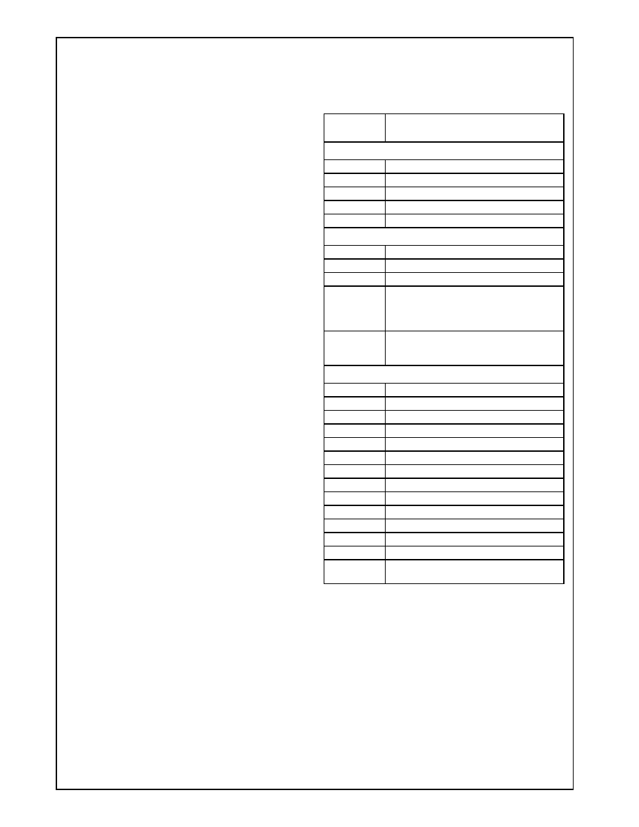
www.national.com
212
Revision 3.1
Instruction Set (
Continued
)
GeodeTM
G
Xm
Pr
ocessor
9.3
PROCESSOR CORE INSTRUCTION SET
The instruction set for the GXm processor core is summa-
rized in Table 9-27 on page 213. The table uses several
symbols and abbreviations that are described next and
listed in Table 9-26.
Opcodes
Opcodes are given as hex values except when they
appear within brackets as binary values.
Clock Counts
The clock counts listed in the instruction set summary
table are grouped by operating mode (Real and Pro-
tected) and whether there is a register/cache hit or a
cache miss. In some cases, more than one clock count is
shown in a column for a given instruction, or a variable is
used in the clock count.
Flags
There are nine flags that are affected by the execution of
instructions. The flag names have been abbreviated and vari-
ous conventions used to indicate what effect the instruc-
tion has on the particular flag.
Table 9-26. Processor Core Instruction Set
Table Legend
Symbol or
Abbreviation
Description
Opcode
#
Immediate 8-bit data
##
Immediate 16-bit data
###
Full immediate 32-bit data (8, 16, 32 bits)
+
8-bit signed displacement
+++
Full signed displacement (16, 32 bits)
Clock Count
/
Register operand/memory operand.
n
Number of times operation is repeated.
L
Level of the stack frame.
|
Conditional jump taken | Conditional jump not
taken.
(e.g. "4|1" = 4 clocks if jump taken, 1 clock if
jump not taken)
\
CPL
IOPL \ CPL > IOPL
(where CPL = Current Privilege Level, IOPL =
I/O Privilege Level)
Flags
OF
Overflow Flag
DF
Direction Flag
IF
Interrupt Enable Flag
TF
Trap Flag
SF
Sign Flag
ZF
Zero Flag
AF
Auxiliary Flag
PF
Parity Flag
CF
Carry Flag
x
Flag is modified by the instruction.
-
Flag is not changed by the instruction.
0
Flag is reset to "0".
1
Flag is set to "1".
u
Flag is undefined following execution the
instruction.
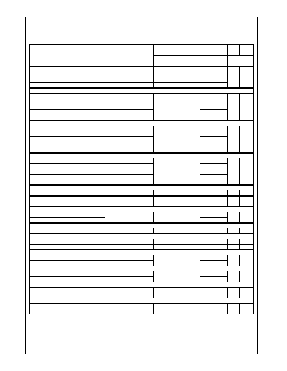
Revision 3.1
213
www.national.com
Instruction Set (
Continued
)
GeodeTM
G
Xm
P
r
ocessor
Table 9-27. Processor Core Instruction Set Summary
Instruction
Opcode
Flags
Real
Mode
Prot'd
Mode
Real
Mode
Prot'd
Mode
O D I
T
S Z
A P C
F
F
F
F
F
F
F
F
F
Clock Count
(Reg/Cache Hit)
Notes
AAA ASCII Adjust AL after Add
37
u
-
-
-
u
u
x
u
x
3
3
AAD ASCII Adjust AX before Divide
D5 0A
u
-
-
-
x
x
u
x
u
7
7
AAM ASCII Adjust AX after Multiply
D4 0A
u
-
-
-
x
x
u
x
u
19
19
AAS ASCII Adjust AL after Subtract
3F
u
-
-
-
u
u
x
u
x
3
3
ADC Add with Carry
Register to Register
1 [00dw] [11 reg r/m]
x
-
-
-
x
x
x
x
x
1
1
b
h
Register to Memory
1 [000w] [mod reg r/m]
1
1
Memory to Register
1 [001w] [mod reg r/m]
1
1
Immediate to Register/Memory
8 [00sw] [mod 010 r/m]###
1
1
Immediate to Accumulator
1 [010w] ###
1
1
ADD Integer Add
Register to Register
0 [00dw] [11 reg r/m]
x
-
-
-
x
x
x
x
x
1
1
b
h
Register to Memory
0 [000w] [mod reg r/m]
1
1
Memory to Register
0 [001w] [mod reg r/m]
1
1
Immediate to Register/Memory
8 [00sw] [mod 000 r/m]###
1
1
Immediate to Accumulator
0 [010w] ###
1
1
AND Boolean AND
Register to Register
2 [00dw] [11 reg r/m]
0
-
-
-
x
x
u
x
0
1
1
b
h
Register to Memory
2 [000w] [mod reg r/m]
1
1
Memory to Register
2 [001w] [mod reg r/m]
1
1
Immediate to Register/Memory
8 [00sw] [mod 100 r/m]###
1
1
Immediate to Accumulator
2 [010w] ###
1
1
ARPL Adjust Requested Privilege Level
From Register/Memory
63 [mod reg r/m]
-
-
-
-
-
x
-
-
-
9
a
h
BB0_Reset Set BLT Buffer 0 Pointer to the Base
0F 3A
2
2
BB1_Reset Set BLT Buffer 1 Pointer to the Base
0F 3B
2
2
BOUND Check Array Boundaries
If Out of Range (Int 5)
62 [mod reg r/m]
-
-
-
-
-
-
-
-
-
8+INT
8+INT
b, e
g,h,j,k,r
If In Range
7
7
BSF Scan Bit Forward
Register, Register/Memory
0F BC [mod reg r/m]
-
-
-
-
-
x
-
-
-
4/9+n
4/9+n
b
h
BSR Scan Bit Reverse
Register, Register/Memory
0F BD [mod reg r/m]
-
-
-
-
-
x
-
-
-
4/11+n
4/11+n
b
h
BSWAP Byte Swap
0F C[1 reg]
-
-
-
-
-
-
-
-
-
6
6
BT Test Bit
Register/Memory, Immediate
0F BA [mod 100 r/m]#
-
-
-
-
-
-
-
-
x
1
1
b
h
Register/Memory, Register
0F A3 [mod reg r/m]
1/7
1/7
BTC Test Bit and Complement
Register/Memory, Immediate
0F BA [mod 111 r/m]#
-
-
-
-
-
-
-
-
x
2
2
b
h
Register/Memory, Register
0F BB [mod reg r/m]
2/8
2/8
BTR Test Bit and Reset
Register/Memory, Immediate
0F BA [mod 110 r/m]#
-
-
-
-
-
-
-
-
x
2
2
b
h
Register/Memory, Register
0F B3 [mod reg r/m
2/8
2/8
BTS Test Bit and Set
Register/Memory
0F BA [mod 101 r/m]
-
-
-
-
-
-
-
-
x
2
2
b
h
Register (short form)
0F AB [mod reg r/m]
2/8
2/8
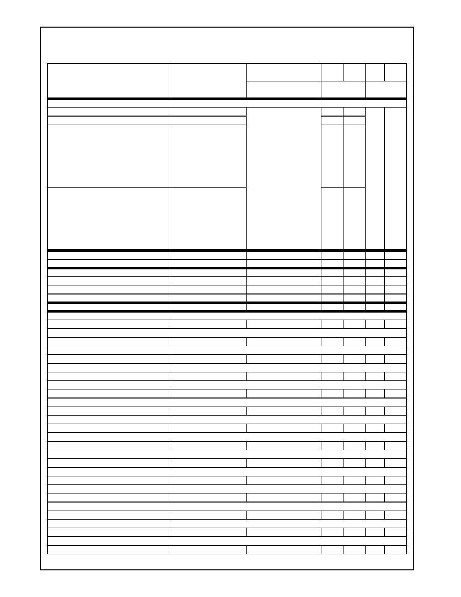
www.national.com
214
Revision 3.1
Instruction Set (
Continued
)
GeodeTM
G
Xm
Pr
ocessor
CALL Subroutine Call
Direct Within Segment
E8 +++
-
-
-
-
-
-
-
-
-
3
3
b
h,j,k,r
Register/Memory Indirect Within Segment
FF [mod 010 r/m]
3/4
3/4
Direct Intersegment
-Call Gate to Same Privilege
-Call Gate to Different Privilege No Par's
-Call Gate to Different Privilege m Par's
-16-bit Task to 16-bit TSS
-16-bit Task to 32-bit TSS
-16-bit Task to V86 Task
-32-bit Task to 16-bit TSS
-32-bit Task to 32-bit TSS
-32-bit Task to V86 Task
9A [unsigned full offset,
selector]
9
14
24
45
51+2m
183
189
123
186
192
126
Indirect Intersegment
-Call Gate to Same Privilege
-Call Gate to Different Privilege No Par's
-Call Gate to Different Privilege m Par's
-16-bit Task to 16-bit TSS
-16-bit Task to 32-bit TSS
-16-bit Task to V86 Task
-32-bit Task to 16-bit TSS
-32-bit Task to 32-bit TSS
-32-bit Task to V86 Task
FF [mod 011 r/m]
11
15
25
46
52+2m
184
190
124
187
193
127
CBW Convert Byte to Word
98
-
-
-
-
-
-
-
-
-
3
3
CDQ Convert Doubleword to Quadword
99
-
-
-
-
-
-
-
-
-
2
2
CLC Clear Carry Flag
F8
-
-
-
-
-
-
-
-
0
1
1
CLD Clear Direction Flag
FC
-
0
-
-
-
-
-
-
-
4
4
CLI Clear Interrupt Flag
FA
-
-
0
-
-
-
-
-
-
6
6
m
CLTS Clear Task Switched Flag
0F 06
-
-
-
-
-
-
-
-
-
7
7
c
l
CMC Complement the Carry Flag
F5
-
-
-
-
-
-
-
-
x
3
3
CMOVA/CMOVNBE Move if Above/Not Below or Equal
Register, Register/Memory
0F 47 [mod reg r/m]
-
-
-
-
-
-
-
-
-
1
1
r
CMOVBE/CMOVNA Move if Below or Equal/Not Above
Register, Register/Memory
0F 46 [mod reg r/m]
-
-
-
-
-
-
-
-
-
1
1
r
CMOVAE/CMOVNB/CMOVNC Move if Above or Equal/Not Below/Not Carry
Register, Register/Memory
0F 43 [mod reg r/m]
-
-
-
-
-
-
-
-
-
1
1
r
CMOVB/CMOVC/CMOVNAE Move if Below/Carry/Not Above or Equal
Register, Register/Memory
0F 42 [mod reg r/m]
-
-
-
-
-
-
-
-
-
1
1
r
CMOVE/CMOVZ Move if Equal/Zero
Register, Register/Memory
0F 44 [mod reg r/m]
-
-
-
-
-
-
-
-
-
1
1
r
CMOVNE/CMOVNZ Move if Not Equal/Not Zero
Register, Register/Memory
0F 45 [mod reg r/m]
-
-
-
-
-
-
-
-
-
1
1
r
CMOVG/CMOVNLE Move if Greater/Not Less or Equal
Register, Register/Memory
0F 4F [mod reg r/m]
-
-
-
-
-
-
-
-
-
1
1
r
CMOVLE/CMOVNG Move if Less or Equal/Not Greater
Register, Register/Memory
0F 4E [mod reg r/m]
-
-
-
-
-
-
-
-
-
1
1
r
CMOVL/CMOVNGE Move if Less/Not Greater or Equal
Register, Register/Memory
0F 4C [mod reg r/m]
-
-
-
-
-
-
-
-
-
1
1
r
CMOVGE/CMOVNL Move if Greater or Equal/Not Less
Register, Register/Memory
0F 4D [mod reg r/m]
-
-
-
-
-
-
-
-
-
1
1
r
CMOVO Move if Overflow
Register, Register/Memory
0F 40 [mod reg r/m]
-
-
-
-
-
-
-
-
-
1
1
r
CMOVNO Move if No Overflow
Register, Register/Memory
0F 41 [mod reg r/m]
-
-
-
-
-
-
-
-
-
1
1
r
CMOVP/CMOVPE Move if Parity/Parity Even
Register, Register/Memory
0F 4A [mod reg r/m]
-
-
-
-
-
-
-
-
-
1
1
r
CMOVNP/CMOVPO Move if Not Parity/Parity Odd
Register, Register/Memory
0F 4B [mod reg r/m]
-
-
-
-
-
-
-
-
-
1
1
r
Table 9-27. Processor Core Instruction Set Summary (Continued)
Instruction
Opcode
Flags
Real
Mode
Prot'd
Mode
Real
Mode
Prot'd
Mode
O D I
T
S Z
A P C
F
F
F
F
F
F
F
F
F
Clock Count
(Reg/Cache Hit)
Notes
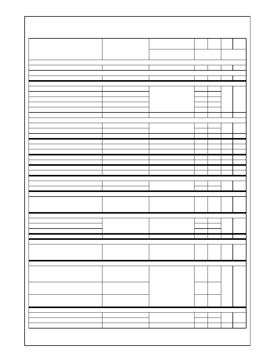
Revision 3.1
215
www.national.com
Instruction Set (
Continued
)
GeodeTM
G
Xm
P
r
ocessor
CMOVS Move if Sign
Register, Register/Memory
0F 48 [mod reg r/m]
-
-
-
-
-
-
-
-
-
1
1
r
CMOVNS Move if Not Sign
Register, Register/Memory
0F 49 [mod reg r/m]
-
-
-
-
-
-
-
-
-
1
1
r
CMP Compare Integers
Register to Register
3 [10dw] [11 reg r/m]
x
-
-
-
x
x
x
x
x
1
1
b
h
Register to Memory
3 [101w] [mod reg r/m]
1
1
Memory to Register
3 [100w] [mod reg r/m]
1
1
Immediate to Register/Memory
8 [00sw] [mod 111 r/m] ###
1
1
Immediate to Accumulator
3 [110w] ###
1
1
CMPS Compare String
A [011w]
x
-
-
-
x
x
x
x
x
6
6
b
h
CMPXCHG Compare and Exchange
Register1, Register2
0F B [000w] [11 reg2 reg1]
x
-
-
-
x
x
x
x
x
6
6
Memory, Register
0F B [000w] [mod reg r/m]
6
6
CMPXCHG8B Compare and Exchange 8 Bytes
0F C7 [mod 001 r/m]
-
-
-
-
-
-
-
-
-
CPUID CPU Identification
0F A2
-
-
-
-
-
-
-
-
-
12
12
CPU_READ Read Special CPU Register
0F 3C
1
1
CPU_WRITE Write Special CPU Register
0F 3D
1
1
CWD Convert Word to Doubleword
99
-
-
-
-
-
-
-
-
-
2
2
CWDE Convert Word to Doubleword Extended
98
-
-
-
-
-
-
-
-
-
3
3
DAA Decimal Adjust AL after Add
27
-
-
-
-
x
x
x
x
x
2
2
DAS Decimal Adjust AL after Subtract
2F
-
-
-
-
x
x
x
x
x
2
2
DEC Decrement by 1
Register/Memory
F [111w] [mod 001 r/m]
x
-
-
-
x
x
x
x
-
1
1
b
h
Register (short form)
4 [1 reg]
1
1
DIV Unsigned Divide
Accumulator by Register/Memory
Divisor:
Byte
Word
Doubleword
F [011w] [mod 110 r/m]
-
-
-
-
x
x
u
u
-
20
29
45
20
29
45
b,e
e,h
ENTER Enter New Stack Frame
Level = 0
C8 ##,#
-
-
-
-
-
-
-
-
-
13
13
b
h
Level = 1
17
17
Level (L) > 1
17+2*L
17+2*L
HLT Halt
F4
-
-
-
-
-
-
-
-
-
10
10
l
IDIV Integer (Signed) Divide
Accumulator by Register/Memory
Divisor:
Byte
Word
Doubleword
F [011w] [mod 111 r/m]
-
-
-
-
x
x
u
u
-
20
29
45
20
29
45
b,e
e,h
IMUL Integer (Signed) Multiply
Accumulator by Register/Memory
Multiplier:
Byte
Word
Doubleword
F [011w] [mod 101 r/m]
x
-
-
-
x
x
u
u
x
4
5
15
4
5
15
b
h
Register with Register/Memory
Multiplier:
Word
Doubleword
0F AF [mod reg r/m]
5
15
5
15
Register/Memory with Immediate to Register2
Multiplier:
Word
Doubleword
6 [10s1] [mod reg r/m] ###
6
16
6
16
IN Input from I/O Port
Fixed Port
E [010w] #
-
-
-
-
-
-
-
-
-
8
8/22
m
Variable Port
E [110w]
8
8/22
INS Input String from I/O Port
6 [110w]
-
-
-
-
-
-
-
-
-
11
11/25
b
h,m
Table 9-27. Processor Core Instruction Set Summary (Continued)
Instruction
Opcode
Flags
Real
Mode
Prot'd
Mode
Real
Mode
Prot'd
Mode
O D I
T
S Z
A P C
F
F
F
F
F
F
F
F
F
Clock Count
(Reg/Cache Hit)
Notes

www.national.com
216
Revision 3.1
Instruction Set (
Continued
)
GeodeTM
G
Xm
Pr
ocessor
INC Increment by 1
Register/Memory
F [111w] [mod 000 r/m]
x
-
-
-
x
x
x
x
-
1
1
b
h
Register (short form)
4 [0 reg]
1
1
INT Software Interrupt
INT i
CD #
-
-
x
0
-
-
-
-
-
19
b,e
g,j,k,r
Protected Mode:
-Interrupt or Trap to Same Privilege
-Interrupt or Trap to Different Privilege
-16-bit Task to 16-bit TSS by Task Gate
-16-bit Task to 32-bit TSS by Task Gate
-16-bit Task to V86 by Task Gate
-16-bit Task to 16-bit TSS by Task Gate
-32-bit Task to 32-bit TSS by Task Gate
-32-bit Task to V86 by Task Gate
-V86 to 16-bit TSS by Task Gate
-V86 to 32-bit TSS by Task Gate
-V86 to Privilege 0 by Trap Gate/Int Gate
33
55
184
190
124
187
193
127
187
193
64
INT 3
CC
INT
INT
INTO
If OF==0
If OF==1 (INT 4)
CE
4
INT
4
INT
INVD Invalidate Cache
0F 08
-
-
-
-
-
-
-
-
-
20
20
t
t
INVLPG Invalidate TLB Entry
0F 01 [mod 111 r/m]
-
-
-
-
-
-
-
-
-
15
15
IRET Interrupt Return
Real Mode
CF
x
x
x
x
x
x
x
x
x
13
g,h,j,k,r
Protected Mode:
-Within Task to Same Privilege
-Within Task to Different Privilege
-16-bit Task to 16-bit Task
-16-bit Task to 32-bit TSS
-16-bit Task to V86 Task
-32-bit Task to 16-bit TSS
-32-bit Task to 32-bit TSS
-32-bit Task to V86 Task
20
39
169
175
109
172
178
112
JB/JNAE/JC Jump on Below/Not Above or Equal/Carry
8-bit Displacement
72 +
-
-
-
-
-
-
-
-
-
1
1
r
Full Displacement
0F 82 +++
1
1
JBE/JNA Jump on Below or Equal/Not Above
8-bit Displacement
76 +
-
-
-
-
-
-
-
-
1
1
r
Full Displacement
0F 86 +++
1
1
JCXZ/JECXZ Jump on CX/ECX Zero
E3 +
-
-
-
-
-
-
-
-
-
2
2
r
JE/JZ Jump on Equal/Zero
8-bit Displacement
74 +
-
-
-
-
-
-
-
-
1
1
r
Full Displacement
0F 84 +++
1
1
JL/JNGE Jump on Less/Not Greater or Equal
8-bit Displacement
7C +
-
-
-
-
-
-
-
-
1
1
r
Full Displacement
0F 8C +++
1
1
JLE/JNG Jump on Less or Equal/Not Greater
8-bit Displacement
7E +
-
-
-
-
-
-
-
-
1
1
r
Full Displacement
0F 8E +++
1
1
Table 9-27. Processor Core Instruction Set Summary (Continued)
Instruction
Opcode
Flags
Real
Mode
Prot'd
Mode
Real
Mode
Prot'd
Mode
O D I
T
S Z
A P C
F
F
F
F
F
F
F
F
F
Clock Count
(Reg/Cache Hit)
Notes

Revision 3.1
217
www.national.com
Instruction Set (
Continued
)
GeodeTM
G
Xm
P
r
ocessor
JMP Unconditional Jump
8-bit Displacement
EB +
-
-
-
-
-
-
-
-
1
1
b
h,j,k,r
Full Displacement
E9 +++
1
1
Register/Memory Indirect Within Segment
FF [mod 100 r/m]
1/3
1/3
Direct Intersegment
-Call Gate Same Privilege Level
-16-bit Task to 16-bit TSS
-16-bit Task to 32-bit TSS
-16-bit Task to V86 Task
-32-bit Task to 16-bit TSS
-32-bit Task to 32-bit TSS
-32-bit Task to V86 Task
EA [unsigned full offset,
selector]
8
12
22
186
192
126
189
195
129
Indirect Intersegment
-Call Gate Same Privilege Level
-16-bit Task to 16-bit TSS
-16-bit Task to 32-bit TSS
-16-bit Task to V86 Task
-32-bit Task to 16-bit TSS
-32-bit Task to 32-bit TSS
-32-bit Task to V86 Task
FF [mod 101 r/m]
10
13
23
187
193
127
190
196
130
JNB/JAE/JNC Jump on Not Below/Above or Equal/Not Carry
8-bit Displacement
73 +
-
-
-
-
-
-
-
-
1
1
r
Full Displacement
0F 83 +++
1
1
JNBE/JA Jump on Not Below or Equal/Above
8-bit Displacement
77 +
-
-
-
-
-
-
-
-
1
1
r
Full Displacement
0F 87 +++
1
1
JNE/JNZ Jump on Not Equal/Not Zero
8-bit Displacement
75 +
-
-
-
-
-
-
-
-
1
1
r
Full Displacement
0F 85 +++
1
1
JNL/JGE Jump on Not Less/Greater or Equal
8-bit Displacement
7D +
-
-
-
-
-
-
-
-
1
1
r
Full Displacement
0F 8D +++
1
1
JNLE/JG Jump on Not Less or Equal/Greater
8-bit Displacement
7F +
-
-
-
-
-
-
-
-
1
1
r
Full Displacement
0F 8F +++
1
1
JNO Jump on Not Overflow
8-bit Displacement
71 +
-
-
-
-
-
-
-
-
1
1
r
Full Displacement
0F 81 +++
1
1
JNP/JPO Jump on Not Parity/Parity Odd
8-bit Displacement
7B +
-
-
-
-
-
-
-
-
1
1
r
Full Displacement
0F 8B +++
1
1
JNS Jump on Not Sign
8-bit Displacement
79 +
-
-
-
-
-
-
-
-
1
1
r
Full Displacement
0F 89 +++
1
1
JO Jump on Overflow
8-bit Displacement
70 +
-
-
-
-
-
-
-
-
1
1
r
Full Displacement
0F 80 +++
1
1
JP/JPE Jump on Parity/Parity Even
8-bit Displacement
7A +
-
-
-
-
-
-
-
-
1
1
r
Full Displacement
0F 8A +++
1
1
JS Jump on Sign
8-bit Displacement
78 +
-
-
-
-
-
-
-
-
1
1
r
Full Displacement
0F 88 +++
1
1
LAHF Load AH with Flags
9F
-
-
-
-
-
-
-
-
-
2
2
LAR Load Access Rights
From Register/Memory
0F 02 [mod reg r/m]
-
-
-
-
-
x
-
-
-
9
a
g,h,j,p
LDS Load Pointer to DS
C5 [mod reg r/m]
-
-
-
-
-
-
-
-
-
4
9
b
h,i,j
Table 9-27. Processor Core Instruction Set Summary (Continued)
Instruction
Opcode
Flags
Real
Mode
Prot'd
Mode
Real
Mode
Prot'd
Mode
O D I
T
S Z
A P C
F
F
F
F
F
F
F
F
F
Clock Count
(Reg/Cache Hit)
Notes

www.national.com
218
Revision 3.1
Instruction Set (
Continued
)
GeodeTM
G
Xm
Pr
ocessor
LEA Load Effective Address
No Index Register
8D [mod reg r/m]
-
-
-
-
-
-
-
-
-
1
1
With Index Register
1
1
LES Load Pointer to ES
C4 [mod reg r/m]
-
-
-
-
-
-
-
-
-
4
9
b
h,i,j
LFS Load Pointer to FS
0F B4 [mod reg r/m]
-
-
-
-
-
-
-
-
-
4
9
b
h,i,j
LGDT Load GDT Register
0F 01 [mod 010 r/m]
-
-
-
-
-
-
-
-
-
10
10
b,c
h,l
LGS Load Pointer to GS
0F B5 [mod reg r/m]
-
-
-
-
-
-
-
-
-
4
9
b
h,i,j
LIDT Load IDT Register
0F 01 [mod 011 r/m]
-
-
-
-
-
-
-
-
-
10
10
b,c
h,l
LLDT Load LDT Register
From Register/Memory
0F 00 [mod 010 r/m]
-
-
-
-
-
-
-
-
-
8
a
g,h,j,l
LMSW Load Machine Status Word
From Register/Memory
0F 01 [mod 110 r/m]
-
-
-
-
-
-
-
-
-
11
11
b,c
h,l
LODS Load String
A [110 w]
-
-
-
-
-
-
-
-
-
3
3
b
h
LSL Load Segment Limit
From Register/Memory
0F 03 [mod reg r/m]
-
-
-
-
-
x
-
-
-
9
a
g,h,j,p
LSS Load Pointer to SS
0F B2 [mod reg r/m]
-
-
-
-
-
-
-
-
-
4
10
a
h,i,j
LTR Load Task Register
From Register/Memory
0F 00 [mod 011 r/m]
-
-
-
-
-
-
-
-
-
9
a
g,h,j,l
LEAVE Leave Current Stack Frame
C9
-
-
-
-
-
-
-
-
-
4
4
b
h
LOOP Offset Loop/No Loop
E2 +
-
-
-
-
-
-
-
-
-
2
2
r
LOOPNZ/LOOPNE Offset
E0 +
-
-
-
-
-
-
-
-
-
2
2
r
LOOPZ/LOOPE Offset
E1 +
-
-
-
-
-
-
-
-
-
2
2
r
MOV Move Data
Register to Register
8 [10dw] [11 reg r/m]
-
-
-
-
-
-
-
-
-
1
1
b
h,i,j
Register to Memory
8 [100w] [mod reg r/m]
1
1
Register/Memory to Register
8 [101w] [mod reg r/m]
1
1
Immediate to Register/Memory
C [011w] [mod 000 r/m] ###
1
1
Immediate to Register (short form)
B [w reg] ###
1
1
Memory to Accumulator (short form)
A [000w] +++
1
1
Accumulator to Memory (short form)
A [001w] +++
1
1
Register/Memory to Segment Register
8E [mod sreg3 r/m]
1
6
Segment Register to Register/Memory
8C [mod sreg3 r/m]
1
1
MOV Move to/from Control/Debug/Test Regs
Register to CR0/CR2/CR3/CR4
0F 22 [11 eee reg]
-
-
-
-
-
-
-
-
-
20/5/5
18/5/6
l
CR0/CR2/CR3/CR4 to Register
0F 20 [11 eee reg]
6
6
Register to DR0-DR3
0F 23 [11 eee reg]
10
10
DR0-DR3 to Register
0F 21 [11 eee reg]
9
9
Register to DR6-DR7
0F 23 [11 eee reg]
10
10
DR6-DR7 to Register
0F 21 [11 eee reg]
9
9
Register to TR3-5
0F 26 [11 eee reg]
16
16
TR3-5 to Register
0F 24 [11 eee reg]
8
8
Register to TR6-TR7
0F 26 [11 eee reg]
11
11
TR6-TR7 to Register
0F 24 [11 eee reg]
3
3
MOVS Move String
A [010w]
-
-
-
-
-
-
-
-
-
6
6
b
h
MOVSX Move with Sign Extension
Register from Register/Memory
0F B[111w] [mod reg r/m]
-
-
-
-
-
-
-
-
-
1
1
b
h
MOVZX Move with Zero Extension
Register from Register/Memory
0F B[011w] [mod reg r/m]
-
-
-
-
-
-
-
-
-
1
1
b
h
MUL Unsigned Multiply
Accumulator with Register/Memory
Multiplier:
Byte
Word
Doubleword
F [011w] [mod 100 r/m]
x
-
-
-
x
x
u
u
x
4
5
15
4
5
15
b
h
Table 9-27. Processor Core Instruction Set Summary (Continued)
Instruction
Opcode
Flags
Real
Mode
Prot'd
Mode
Real
Mode
Prot'd
Mode
O D I
T
S Z
A P C
F
F
F
F
F
F
F
F
F
Clock Count
(Reg/Cache Hit)
Notes
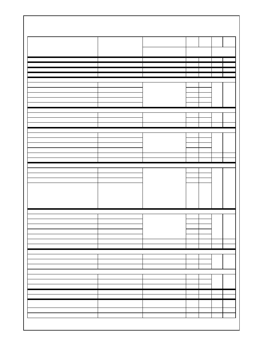
Revision 3.1
219
www.national.com
Instruction Set (
Continued
)
GeodeTM
G
Xm
P
r
ocessor
NEG Negate Integer
F [011w] [mod 011 r/m]
x
-
-
-
x
x
x
x
x
1
1
b
h
NOP No Operation
90
-
-
-
-
-
-
-
-
-
1
1
NOT Boolean Complement
F [011w] [mod 010 r/m]
-
-
-
-
-
-
-
-
-
1
1
b
h
OIO Official Invalid Opcode
0F FF
-
-
x
0
-
-
-
-
-
1
8-125
OR Boolean OR
Register to Register
0 [10dw] [11 reg r/m]
0
-
-
-
x
x
u
x
0
1
1
b
h
Register to Memory
0 [100w] [mod reg r/m]
1
1
Memory to Register
0 [101w] [mod reg r/m]
1
1
Immediate to Register/Memory
8 [00sw] [mod 001 r/m] ###
1
1
Immediate to Accumulator
0 [110w] ###
1
1
OUT Output to Port
Fixed Port
E [011w] #
-
-
-
-
-
-
-
-
-
14
14/28
m
Variable Port
E [111w]
14
14/28
OUTS Output String
6 [111w]
-
-
-
-
-
-
-
-
-
15
15/29
b
h,m
POP Pop Value off Stack
Register/Memory
8F [mod 000 r/m]
-
-
-
-
-
-
-
-
-
1/4
1/4
b
h,i,j
Register (short form)
5 [1 reg]
1
1
Segment Register (ES, SS, DS)
[000 sreg2 111]
1
6
Segment Register (FS, GS)
0F [10 sreg3 001]
1
6
POPA Pop All General Registers
61
-
-
-
-
-
-
-
-
-
9
9
b
h
POPF Pop Stack into FLAGS
9D
x
x
x
x
x
x
x
x
x
8
8
b
h,n
PREFIX BYTES
Assert Hardware LOCK Prefix
F0
-
-
-
-
-
-
-
-
-
m
Address Size Prefix
67
Operand Size Prefix
66
Segment Override Prefix
-CS
-DS
-ES
-FS
-GS
-SS
2E
3E
26
64
65
36
PUSH Push Value onto Stack
Register/Memory
FF [mod 110 r/m]
-
-
-
-
-
-
-
-
-
1/3
1/3
b
h
Register (short form)
5 [0 reg]
1
1
Segment Register (ES, CS, SS, DS)
[000 sreg2 110]
1
1
Segment Register (FS, GS)
0F [10 sreg3 000]
1
1
Immediate
6 [10s0] ###
1
1
PUSHA Push All General Registers
60
-
-
-
-
-
-
-
-
-
11
11
b
h
PUSHF Push FLAGS Register
9C
-
-
-
-
-
-
-
-
-
2
2
b
h
RCL Rotate Through Carry Left
Register/Memory by 1
D [000w] [mod 010 r/m]
x
-
-
-
-
-
-
-
x
3
3
b
h
Register/Memory by CL
D [001w] [mod 010 r/m]
u
-
-
-
-
-
-
-
x
8
8
Register/Memory by Immediate
C [000w] [mod 010 r/m] #
u
-
-
-
-
-
-
-
x
8
8
RCR Rotate Through Carry Right
Register/Memory by 1
D [000w] [mod 011 r/m]
x
-
-
-
-
-
-
-
x
4
4
b
h
Register/Memory by CL
D [001w] [mod 011 r/m]
u
-
-
-
-
-
-
-
x
8
8
Register/Memory by Immediate
C [000w] [mod 011 r/m] #
u
-
-
-
-
-
-
-
x
8
8
RDMSR Read Tmodel Specific Register
0F 32
-
-
-
-
-
-
-
-
-
RDTSC Read Time Stamp Counter
0F 31
-
-
-
-
-
-
-
-
-
REP INS Input String
F3 6[110w]
-
-
-
-
-
-
-
-
-
17+4n
17+4n\
32+4n
b
h,m
REP LODS Load String
F3 A[110w]
-
-
-
-
-
-
-
-
-
9+2n
9+2n
b
h
REP MOVS Move String
F3 A[010w]
-
-
-
-
-
-
-
-
-
12+2n
12+2n
b
h
Table 9-27. Processor Core Instruction Set Summary (Continued)
Instruction
Opcode
Flags
Real
Mode
Prot'd
Mode
Real
Mode
Prot'd
Mode
O D I
T
S Z
A P C
F
F
F
F
F
F
F
F
F
Clock Count
(Reg/Cache Hit)
Notes
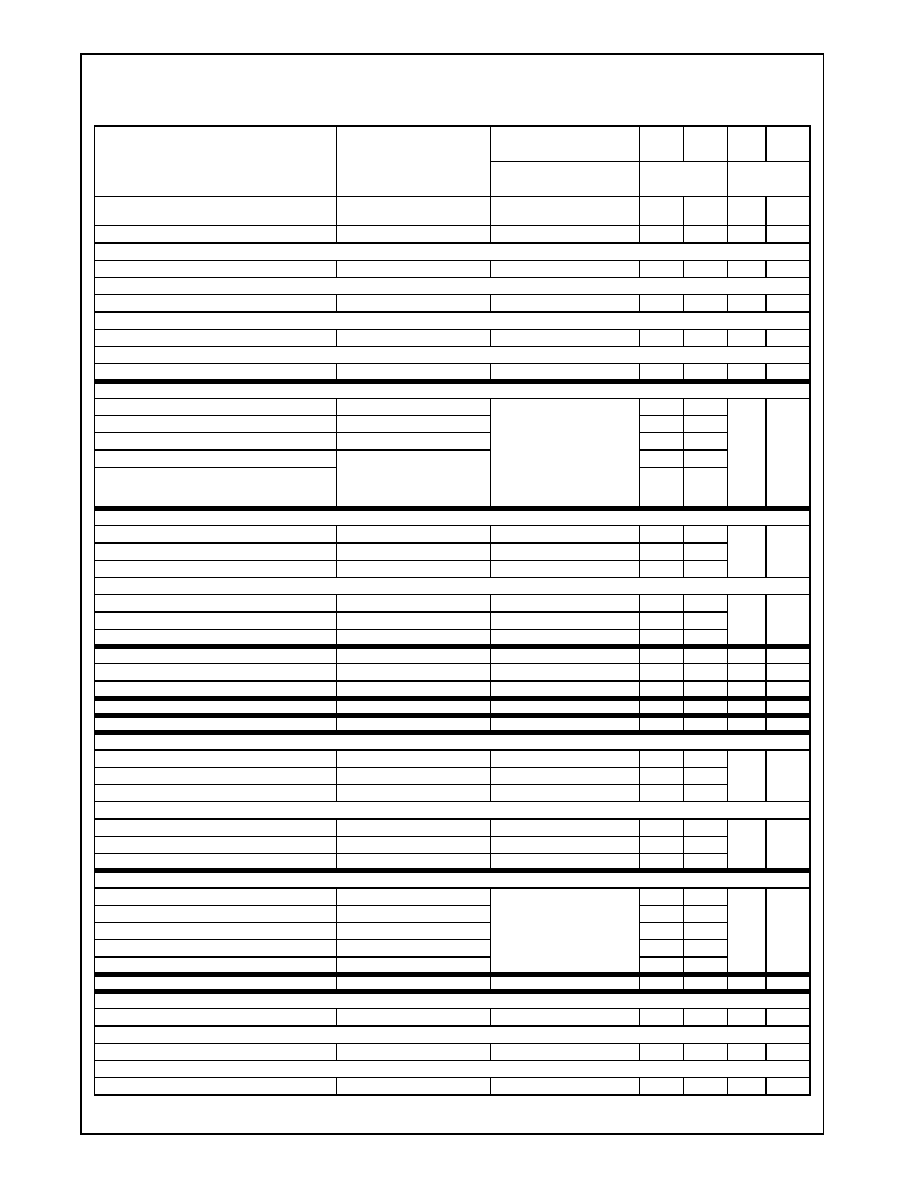
www.national.com
220
Revision 3.1
Instruction Set (
Continued
)
GeodeTM
G
Xm
Pr
ocessor
REP OUTS Output String
F3 6[111w]
-
-
-
-
-
-
-
-
-
24+4n
24+4n\
39+4n
b
h,m
REP STOS Store String
F3 A[101w]
-
-
-
-
-
-
-
-
-
9+2n
9+2n
b
h
REPE CMPS Compare String
Find non-match
F3 A[011w]
x
-
-
-
x
x
x
x
x
11+4n
11+4n
b
h
REPE SCAS Scan String
Find non-AL/AX/EAX
F3 A[111w]
x
-
-
-
x
x
x
x
x
9+3n
9+3n
b
h
REPNE CMPS Compare String
Find match
F2 A[011w]
x
-
-
-
x
x
x
x
x
11+4n
11+4n
b
h
REPNE SCAS Scan String
Find AL/AX/EAX
F2 A[111w]
x
-
-
-
x
x
x
x
x
9+3n
9+3n
b
h
RET Return from Subroutine
Within Segment
C3
-
-
-
-
-
-
-
-
-
3
3
b
g,h,j,k,r
Within Segment Adding Immediate to SP
C2 ##
3
3
Intersegment
CB
10
13
Intersegment Adding Immediate to SP
CA ##
10
13
Protected Mode: Different Privilege Level
-Intersegment
-Intersegment Adding Immediate to SP
35
35
ROL Rotate Left
Register/Memory by 1
D[000w] [mod 000 r/m]
x
-
-
-
-
-
-
-
x
2
2
b
h
Register/Memory by CL
D[001w] [mod 000 r/m]
u
-
-
-
-
-
-
-
x
2
2
Register/Memory by Immediate
C[000w] [mod 000 r/m] #
u
-
-
-
-
-
-
-
x
2
2
ROR Rotate Right
Register/Memory by 1
D[000w] [mod 001 r/m]
x
-
-
-
-
-
-
-
x
2
2
b
h
Register/Memory by CL
D[001w] [mod 001 r/m]
u
-
-
-
-
-
-
-
x
2
2
Register/Memory by Immediate
C[000w] [mod 001 r/m] #
u
-
-
-
-
-
-
-
x
2
2
RSDC Restore Segment Register and Descriptor
0F 79 [mod sreg3 r/m]
-
-
-
-
-
-
-
-
-
11
11
s
s
RSLDT Restore LDTR and Descriptor
0F 7B [mod 000 r/m]
-
-
-
-
-
-
-
-
-
11
11
s
s
RSTS Restore TSR and Descriptor
0F 7D [mod 000 r/m]
-
-
-
-
-
-
-
-
-
11
11
s
s
RSM Resume from SMM Mode
0F AA
x
x
x
x
x
x
x
x
x
57
57
s
s
SAHF Store AH in FLAGS
9E
-
-
-
-
x
x
x
x
x
1
1
SAL Shift Left Arithmetic
Register/Memory by 1
D[000w] [mod 100 r/m]
x
-
-
-
x
x
u
x
x
1
1
b
h
Register/Memory by CL
D[001w] [mod 100 r/m]
u
-
-
-
x
x
u
x
x
2
2
Register/Memory by Immediate
C[000w] [mod 100 r/m] #
u
-
-
-
x
x
u
x
x
1
1
SAR Shift Right Arithmetic
Register/Memory by 1
D[000w] [mod 111 r/m]
x
-
-
-
x
x
u
x
x
2
2
b
h
Register/Memory by CL
D[001w] [mod 111 r/m]
u
-
-
-
x
x
u
x
x
2
2
Register/Memory by Immediate
C[000w] [mod 111 r/m] #
u
-
-
-
x
x
u
x
x
2
2
SBB Integer Subtract with Borrow
Register to Register
1[10dw] [11 reg r/m]
x
-
-
-
x
x
x
x
x
1
1
b
h
Register to Memory
1[100w] [mod reg r/m]
1
1
Memory to Register
1[101w] [mod reg r/m]
1
1
Immediate to Register/Memory
8[00sw] [mod 011 r/m] ###
1
1
Immediate to Accumulator (short form)
1[110w] ###
1
1
SCAS Scan String
A [111w]
x
-
-
-
x
x
x
x
x
2
2
b
h
SETB/SETNAE/SETC Set Byte on Below/Not Above or Equal/Carry
To Register/Memory
0F 92 [mod 000 r/m]
-
-
-
-
-
-
-
-
-
1
1
h
SETBE/SETNA Set Byte on Below or Equal/Not Above
To Register/Memory
0F 96 [mod 000 r/m]
-
-
-
-
-
-
-
-
-
1
1
h
SETE/SETZ Set Byte on Equal/Zero
To Register/Memory
0F 94 [mod 000 r/m]
-
-
-
-
-
-
-
-
-
1
1
h
Table 9-27. Processor Core Instruction Set Summary (Continued)
Instruction
Opcode
Flags
Real
Mode
Prot'd
Mode
Real
Mode
Prot'd
Mode
O D I
T
S Z
A P C
F
F
F
F
F
F
F
F
F
Clock Count
(Reg/Cache Hit)
Notes

Revision 3.1
221
www.national.com
Instruction Set (
Continued
)
GeodeTM
G
Xm
P
r
ocessor
SETL/SETNGE Set Byte on Less/Not Greater or Equal
To Register/Memory
0F 9C [mod 000 r/m]
-
-
-
-
-
-
-
-
-
1
1
h
SETLE/SETNG Set Byte on Less or Equal/Not Greater
To Register/Memory
0F 9E [mod 000 r/m]
-
-
-
-
-
-
-
-
-
1
1
h
SETNB/SETAE/SETNC Set Byte on Not Below/Above or Equal/Not Carry
To Register/Memory
0F 93 [mod 000 r/m]
-
-
-
-
-
-
-
-
-
1
1
h
SETNBE/SETA Set Byte on Not Below or Equal/Above
To Register/Memory
0F 97 [mod 000 r/m]
-
-
-
-
-
-
-
-
-
1
1
h
SETNE/SETNZ Set Byte on Not Equal/Not Zero
To Register/Memory
0F 95 [mod 000 r/m]
-
-
-
-
-
-
-
-
-
1
1
h
SETNL/SETGE Set Byte on Not Less/Greater or Equal
To Register/Memory
0F 9D [mod 000 r/m]
-
-
-
-
-
-
-
-
-
1
1
h
SETNLE/SETG Set Byte on Not Less or Equal/Greater
To Register/Memory
0F 9F [mod 000 r/m]
-
-
-
-
-
-
-
-
-
1
1
h
SETNO Set Byte on Not Overflow
To Register/Memory
0F 91 [mod 000 r/m]
-
-
-
-
-
-
-
-
-
1
1
h
SETNP/SETPO Set Byte on Not Parity/Parity Odd
To Register/Memory
0F 9B [mod 000 r/m]
-
-
-
-
-
-
-
-
-
1
1
h
SETNS Set Byte on Not Sign
To Register/Memory
0F 99 [mod 000 r/m]
-
-
-
-
-
-
-
-
-
1
1
h
SETO Set Byte on Overflow
To Register/Memory
0F 90 [mod 000 r/m]
-
-
-
-
-
-
-
-
-
1
1
h
SETP/SETPE Set Byte on Parity/Parity Even
To Register/Memory
0F 9A [mod 000 r/m]
-
-
-
-
-
-
-
-
-
1
1
h
SETS Set Byte on Sign
To Register/Memory
0F 98 [mod 000 r/m]
-
-
-
-
-
-
-
-
-
1
1
h
SGDT Store GDT Register
To Register/Memory
0F 01 [mod 000 r/m]
-
-
-
-
-
-
-
-
-
6
6
b,c
h
SIDT Store IDT Register
To Register/Memory
0F 01 [mod 001 r/m]
-
-
-
-
-
-
-
-
-
6
6
b,c
h
SLDT Store LDT Register
To Register/Memory
0F 00 [mod 000 r/m]
-
-
-
-
-
-
-
-
-
1
a
h
STR Store Task Register
To Register/Memory
0F 00 [mod 001 r/m]
-
-
-
-
-
-
-
-
-
3
a
h
SMSW Store Machine Status Word
0F 01 [mod 100 r/m]
-
-
-
-
-
-
-
-
-
4
4
b,c
h
STOS Store String
A [101w]
-
-
-
-
-
-
-
-
-
2
2
b
h
SHL Shift Left Logical
Register/Memory by 1
D [000w] [mod 100 r/m]
x
-
-
-
x
x
u
x
x
1
1
b
h
Register/Memory by CL
D [001w] [mod 100 r/m]
u
-
-
-
x
x
u
x
x
2
2
Register/Memory by Immediate
C [000w] [mod 100 r/m] #
u
-
-
-
x
x
u
x
x
1
1
SHLD Shift Left Double
Register/Memory by Immediate
0F A4 [mod reg r/m] #
u
-
-
-
x
x
u
x
x
3
3
b
h
Register/Memory by CL
0F A5 [mod reg r/m]
6
6
SHR Shift Right Logical
Register/Memory by 1
D [000w] [mod 101 r/m]
x
-
-
-
x
x
u
x
x
2
2
b
h
Register/Memory by CL
D [001w] [mod 101 r/m]
u
-
-
-
x
x
u
x
x
2
2
Register/Memory by Immediate
C [000w] [mod 101 r/m] #
u
-
-
-
x
x
u
x
x
2
2
SHRD Shift Right Double
Register/Memory by Immediate
0F AC [mod reg r/m] #
u
-
-
-
x
x
u
x
x
3
3
b
h
Register/Memory by CL
0F AD [mod reg r/m]
6
6
SMINT Software SMM Entry
0F 38
-
-
-
-
-
-
-
-
-
84
84
s
s
Table 9-27. Processor Core Instruction Set Summary (Continued)
Instruction
Opcode
Flags
Real
Mode
Prot'd
Mode
Real
Mode
Prot'd
Mode
O D I
T
S Z
A P C
F
F
F
F
F
F
F
F
F
Clock Count
(Reg/Cache Hit)
Notes

www.national.com
222
Revision 3.1
Instruction Set (
Continued
)
GeodeTM
G
Xm
Pr
ocessor
STC Set Carry Flag
F9
-
-
-
-
-
-
-
-
1
1
1
STD Set Direction Flag
FD
-
1
-
-
-
-
-
-
-
4
4
STI Set Interrupt Flag
FB
-
-
1
-
-
-
-
-
-
6
6
m
SUB Integer Subtract
Register to Register
2 [10dw] [11 reg r/m]
x
-
-
-
x
x
x
x
x
1
1
b
h
Register to Memory
2 [100w] [mod reg r/m]
1
1
Memory to Register
2 [101w] [mod reg r/m]
1
1
Immediate to Register/Memory
8 [00sw] [mod 101 r/m] ###
1
1
Immediate to Accumulator (short form)
2 [110w] ###
1
1
SVDC Save Segment Register and Descriptor
0F 78 [mod sreg3 r/m]
-
-
-
-
-
-
-
-
-
20
20
s
s
SVLDT Save LDTR and Descriptor
0F 7A [mod 000 r/m]
-
-
-
-
-
-
-
-
-
20
20
s
s
SVTS Save TSR and Descriptor
0F 7C [mod 000 r/m]
-
-
-
-
-
-
-
-
-
21
21
s
s
TEST Test Bits
Register/Memory and Register
8 [010w] [mod reg r/m]
0
-
-
-
x
x
u
x
0
1
1
b
h
Immediate Data and Register/Memory
F [011w] [mod 000 r/m] ###
1
1
Immediate Data and Accumulator
A [100w] ###
1
1
VERR Verify Read Access
To Register/Memory
0F 00 [mod 100 r/m]
-
-
-
-
-
x
-
-
-
8
a
g,h,j,p
VERW Verify Write Access
To Register/Memory
0F 00 [mod 101 r/m]
-
-
-
-
-
x
-
-
-
8
a
g,h,j,p
WAIT Wait Until FPU Not Busy
9B
-
-
-
-
-
-
-
-
-
1
1
WBINVD Write-Back and Invalidate Cache
0F 09
-
-
-
-
-
-
-
-
-
23
23
t
t
WRMSR Write to Model Specific Register
0F 30
-
-
-
-
-
-
-
-
-
XADD Exchange and Add
Register1, Register2
0F C[000w] [11 reg2 reg1]
x
-
-
-
x
x
x
x
x
2
2
Memory, Register
0F C[000w] [mod reg r/m]
2
2
XCHG Exchange
Register/Memory with Register
8[011w] [mod reg r/m]
-
-
-
-
-
-
-
-
-
2
2
b,f
f,h
Register with Accumulator
9[0 reg]
2
2
XLAT Translate Byte
D7
-
-
-
-
-
-
-
-
-
5
5
h
XOR Boolean Exclusive OR
Register to Register
3 [00dw] [11 reg r/m]
0
-
-
-
x
x
u
x
0
1
1
b
h
Register to Memory
3 [000w] [mod reg r/m]
1
1
Memory to Register
3 [001w] [mod reg r/m]
1
1
Immediate to Register/Memory
8 [00sw] [mod 110 r/m] ###
1
1
Immediate to Accumulator (short form)
3 [010w] ###
1
1
Table 9-27. Processor Core Instruction Set Summary (Continued)
Instruction
Opcode
Flags
Real
Mode
Prot'd
Mode
Real
Mode
Prot'd
Mode
O D I
T
S Z
A P C
F
F
F
F
F
F
F
F
F
Clock Count
(Reg/Cache Hit)
Notes

Revision 3.1
223
www.national.com
Instruction Set (
Continued
)
GeodeTM
G
Xm
P
r
ocessor
Instruction Notes for Instruction Set Summary
Notes a through c apply to Real Address Mode only:
a. This is a Protected Mode instruction. Attempted execution in
Real Mode will result in exception 6 (invalid opcode).
b. Exception 13 fault (general protection) will occur in Real
Mode if an operand reference is made that partially or fully
extends beyond the maximum CS, DS, ES, FS, or GS seg-
ment limit (FFFFH). Exception 12 fault (stack segment limit vio-
lation or not present) will occur in Real Mode if an operand
reference is made that partially or fully extends beyond the
maximum SS limit.
c. This instruction may be executed in Real Mode. In Real
Mode, its purpose is primarily to initialize the CPU for Pro-
tected Mode.
d. -
Notes e through g apply to Real Address Mode and Protected
Virtual Address Mode:
e. An exception may occur, depending on the value of the oper-
and.
f.
LOCK# is automatically asserted, regardless of the presence
or absence of the LOCK prefix.
g. LOCK# is asserted during descriptor table accesses.
Notes h through r apply to Protected Virtual Address Mode
only:
h. Exception 13 fault will occur if the memory operand in CS,
DS, ES, FS, or GS cannot be used due to either a segment
limit violation or an access rights violation. If a stack limit is
violated, an exception 12 occurs.
i.
For segment load operations, the CPL, RPL, and DPL must
agree with the privilege rules to avoid an exception 13 fault.
The segment's descriptor must indicate "present" or exception
11 (CS, DS, ES, FS, GS not present). If the SS register is
loaded and a stack segment not present is detected, an
exception 12 occurs.
j.
All segment descriptor accesses in the GDT or LDT made by
this instruction will automatically assert LOCK# to maintain
descriptor integrity in multiprocessor systems.
k. JMP, CALL, INT, RET, and IRET instructions referring to
another code segment will cause an exception 13, if an appli-
cable privilege rule is violated.
l.
An exception 13 fault occurs if CPL is greater than 0 (0 is the
most privileged level).
m. An exception 13 fault occurs if CPL is greater than IOPL.
n. The IF bit of the flag register is not updated if CPL is greater
than IOPL. The IOPL and VM fields of the flag register are
updated only if CPL = 0.
o. The PE bit of the MSW (CR0) cannot be reset by this instruc-
tion. Use MOV into CRO if desiring to reset the PE bit.
p. Any violation of privilege rules as apply to the selector oper-
and does not cause a Protection exception, rather, the zero
flag is cleared.
q. If the coprocessor's memory operand violates a segment limit
or segment access rights, an exception 13 fault will occur
before the ESC instruction is executed. An exception 12 fault
will occur if the stack limit is violated by the operand's starting
address.
r.
The destination of a JMP, CALL, INT, RET, or IRET must be in
the defined limit of a code segment or an exception 13 fault
will occur.
Note s applies to National Semiconductor-specific SMM in-
structions:
s. All memory accesses to SMM space are non-cacheable. An
invalid opcode exception 6 occurs unless SMI is enabled and
SMAR size > 0, and CPL = 0 and [SMAC is set or if in an SMI
handler].
Note t applies to cache invalidation instruction with the
cache operating in write-back mode:
t.
The total clock count is the clock count shown plus the num-
ber of clocks required to write all "modified" cache lines to
external memory.
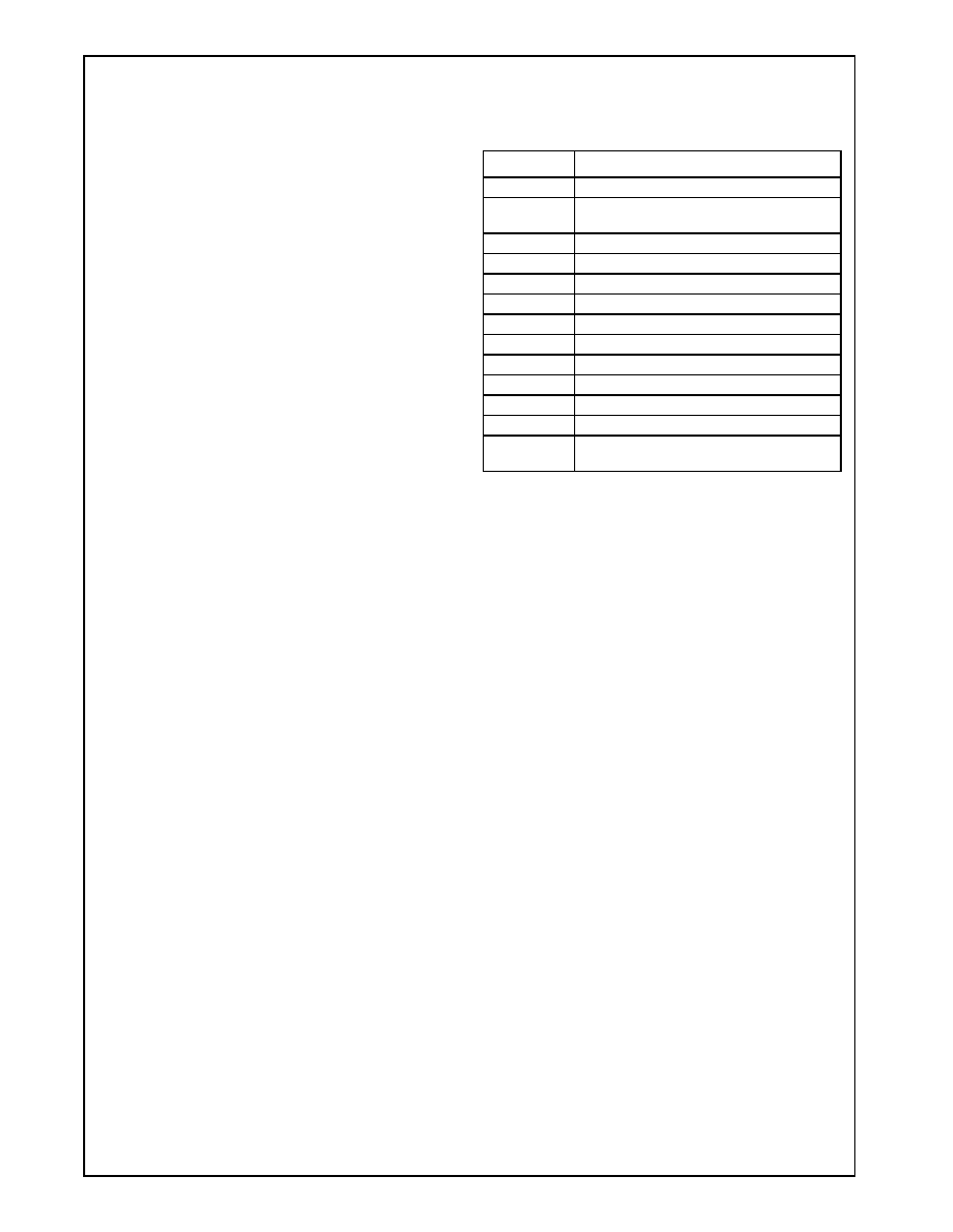
www.national.com
224
Revision 3.1
Instruction Set (
Continued
)
GeodeTM
G
Xm
Pr
ocessor
9.4
FPU INSTRUCTION SET
The processor core is functionally divided into the FPU,
and the integer unit. The FPU processes floating point
instructions only and does so in parallel with the integer
unit.
For example, when the integer unit detects a floating point
instruction without memory operands, after two clock
cycles the instruction passes to the FPU for execution.
The integer unit continues to execute instructions while
the FPU executes the floating point instruction. If another
FPU instruction is encountered, the second FPU instruc-
tion is placed in the FPU queue. Up to four FPU instruc-
tions can be queued. In the event of an FPU exception,
while other FPU instructions are queued, the state of the
CPU is saved to ensure recovery.
The instruction set for the FPU is summarized in Table 9-
29 on page 225. The table uses abbreviations that are
described in Table 9-28.
Table 9-28. FPU Instruction Set Table Legend
Abbr.
Description
n
Stack register number
TOS
Top of stack register pointed to by SSS in the
status register.
ST(1)
FPU register next to TOS
ST(n)
A specific FPU register, relative to TOS
M.WI
16-bit integer operand from memory
M.SI
32-bit integer operand from memory
M.LI
64-bit integer operand from memory
M.SR
32-bit real operand from memory
M.DR
64-bit real operand from memory
M.XR
80-bit real operand from memory
M.BCD
18-digit BCD integer operand from memory
CC
FPU condition code
Env Regs
Status, Mode Control and Tag Registers,
Instruction Pointer and Operand Pointer

Revision 3.1
225
www.national.com
Instruction Set (
Continued
)
GeodeTM
G
Xm
P
r
ocessor
Table 9-29. FPU Instruction Set Summary
FPU Instruction
Opcode
Operation
Clock
Count
Notes
F2XM1 Function Evaluation 2
x
-1
D9 F0
TOS <--- 2
TOS
-1
92 - 108
2
FABS Floating Absolute Value
D9 E1
TOS <--- | TOS |
2
2
FADD Floating Point Add
Top of Stack
DC [1100 0 n]
ST(n) <--- ST(n) + TOS
4 - 9
80-bit Register
D8 [1100 0 n]
TOS <--- TOS + ST(n)
4 - 9
64-bit Real
DC [mod 000 r/m]
TOS <--- TOS + M.DR
4 - 9
32-bit Real
D8 [mod 000 r/m]
TOS <--- TOS + M.SR
4 - 9
FADDP Floating Point Add, Pop
DE [1100 0 n]
ST(n) <--- ST(n) + TOS; then pop TOS
FIADD Floating Point Integer Add
32-bit integer
DA [mod 000 r/m]
TOS <--- TOS + M.SI
8 - 14
16-bit integer
DE [mod 000 r/m]
TOS <--- TOS + M.WI
8 - 14
FCHS Floating Change Sign
D9 E0
TOS <--- - TOS
2
FCLEX Clear Exceptions
(9B) DB E2
Wait then Clear Exceptions
5
FNCLEX Clear Exceptions
DB E2
Clear Exceptions
3
FCMOVB Floating Point Conditional Move if
Below
DA [1100 0 n]
If (CF=1) ST(0) <--- ST(n)
4
FCMOVE Floating Point Conditional Move if
Equal
DA [1100 1 n]
If (ZF=1) ST(0) <--- ST(n)
4
FCMOVBE Floating Point Conditional Move if
Below or Equal
DA [1101 0 n]
If (CF=1 or ZF=1) ST(0) <--- ST(n)
4
FCMOVU Floating Point Conditional Move if
Unordered
DA [1101 1 n]
If (PF=1) ST(0) <--- ST(n)
4
FCMOVNB Floating Point Conditional Move if
Not Below
DB [1100 0 n]
If (CF=0) ST(0) <--- ST(n)
4
FCMOVNE Floating Point Conditional Move if
Not Equal
DB [1100 1 n]
If (ZF=0) ST(0) <--- ST(n)
4
FCMOVNBE Floating Point Conditional Move if
Not Below or Equal
DB [1101 0 n]
If (CF=0 and ZF=0) ST(0) <--- ST(n)
4
FCMOVNU Floating Point Conditional Move if
Not Unordered
DB [1101 1 n]
If (DF=0) ST(0) <--- ST(n)
4
FCOM Floating Point Compare
80-bit Register
D8 [1101 0 n]
CC set by TOS - ST(n)
4
64-bit Real
DC [mod 010 r/m]
CC set by TOS - M.DR
4
32-bit Real
D8 [mod 010 r/m]
CC set by TOS - M.SR
4
FCOMP Floating Point Compare, Pop
80-bit Register
D8 [1101 1 n]
CC set by TOS - ST(n); then pop TOS
4
64-bit Real
DC [mod 011 r/m]
CC set by TOS - M.DR; then pop TOS
4
32-bit Real
D8 [mod 011 r/m]
CC set by TOS - M.SR; then pop TOS
4
FCOMPP Floating Point Compare, Pop
Two Stack Elements
DE D9
CC set by TOS - ST(1); then pop TOS and
ST(1)
4
FCOMI Floating Point Compare Real and Set EFLAGS
80-bit Register
DB [1111 0 n]
EFLAG set by TOS - ST(n)
4
FCOMIP Floating Point Compare Real and Set EFLAGS, Pop
80-bit Register
DF [1111 0 n]
EFLAG set by TOS - ST(n); then pop TOS
4
FUCOMI Floating Point Unordered Compare Real and Set EFLAGS
80-bit Integer
DB [1110 1 n]
EFLAG set by TOS - ST(n)
9 - 10
FUCOMIP Floating Point Unordered Compare Real and Set EFLAGS, Pop
80-bit Integer
DF [1110 1 n]
EFLAG set by TOS - ST(n); then pop TOS
9 - 10
FICOM Floating Point Integer Compare
32-bit integer
DA [mod 010 r/m]
CC set by TOS - M.WI
9 - 10
16-bit integer
DE [mod 010 r/m]
CC set by TOS - M.SI
9 - 10
FICOMP Floating Point Integer Compare, Pop
32-bit integer
DA [mod 011 r/m]
CC set by TOS - M.WI; then pop TOS
9 - 10
16-bit integer
DE [mod 011 r/m
CC set by TOS - M.SI; then pop TOS
9 - 10

www.national.com
226
Revision 3.1
Instruction Set (
Continued
)
GeodeTM
G
Xm
Pr
ocessor
FCOS Function Evaluation: Cos(x)
D9 FF
TOS <--- COS(TOS)
92 - 141
1
FDECSTP Decrement Stack pointer
D9 F6
Decrement top of stack pointer
4
FDIV Floating Point Divide
Top of Stack
DC [1111 1 n]
ST(n) <--- ST(n) / TOS
24 - 34
80-bit Register
D8 [1111 0 n]
TOS <--- TOS / ST(n)
24 - 34
64-bit Real
DC [mod 110 r/m]
TOS <--- TOS / M.DR
24 - 34
32-bit Real
D8 [mod 110 r/m]
TOS <--- TOS / M.SR
24 - 34
FDIVP Floating Point Divide, Pop
DE [1111 1 n]
ST(n) <--- ST(n) / TOS; then pop TOS
24 - 34
FDIVR Floating Point Divide Reversed
Top of Stack
DC [1111 0 n]
TOS <--- ST(n) / TOS
24 - 34
80-bit Register
D8 [1111 1 n]
ST(n) <--- TOS / ST(n)
24 - 34
64-bit Real
DC [mod 111 r/m]
TOS <--- M.DR / TOS
24 - 34
32-bit Real
D8 [mod 111 r/m]
TOS <--- M.SR / TOS
24 - 34
FDIVRP Floating Point Divide Reversed, Pop
DE [1111 0 n]
ST(n) <--- TOS / ST(n); then pop TOS
24 - 34
FIDIV Floating Point Integer Divide
32-bit Integer
DA [mod 110 r/m]
TOS <--- TOS / M.SI
34 - 38
16-bit Integer
DE [mod 110 r/m]
TOS <--- TOS / M.WI
34 - 38
FIDIVR Floating Point Integer Divide Reversed
32-bit Integer
DA [mod 111 r/m]
TOS <--- M.SI / TOS
34 - 38
16-bit Integer
DE [mod 111 r/m]
TOS <--- M.WI / TOS
34 - 38
FFREE Free Floating Point Register
DD [1100 0 n]
TAG(n) <--- Empty
4
FINCSTP Increment Stack Pointer
D9 F7
Increment top-of-stack pointer
2
FINIT Initialize FPU
(9B)DB E3
Wait, then initialize
8
FNINIT Initialize FPU
DB E3
Initialize
6
FLD Load Data to FPU Register
Top of Stack
D9 [1100 0 n]
Push ST(n) onto stack
2
64-bit Real
DD [mod 000 r/m]
Push M.DR onto stack
2
32-bit Real
D9 [mod 000 r/m]
Push M.SR onto stack
2
FBLD Load Packed BCD Data to FPU Register
DF [mod 100 r/m]
Push M.BCD onto stack
41 - 45
FILD Load Integer Data to FPU Register
64-bit Integer
DF [mod 101 r/m]
Push M.LI onto stack
4 - 8
32-bit Integer
DB [mod 000 r/m]
Push M.SI onto stack
4 - 6
16-bit Integer
DF [mod 000 r/m]
Push M.WI onto stack
3 - 6
FLD1 Load Floating Const.= 1.0
D9 E8
Push 1.0 onto stack
4
FLDCW Load FPU Mode Control Register
D9 [mod 101 r/m]
Ctl Word <--- Memory
4
FLDENV Load FPU Environment
D9 [mod 100 r/m]
Env Regs <--- Memory
30
FLDL2E Load Floating Const.= Log
2
(e)
D9 EA
Push Log
2
(e) onto stack
4
FLDL2T Load Floating Const.= Log
2
(10)
D9 E9
Push Log
2
(10) onto stack
4
FLDLG2 Load Floating Const.= Log
10
(2)
D9 EC
Push Log
10
(2) onto stack
4
FLDLN2 Load Floating Const.= Ln(2)
D9 ED
Push Log
e
(2) onto stack
4
FLDPI Load Floating Const.=
D9 EB
Push
onto stack
4
FLDZ Load Floating Const.= 0.0
D9 EE
Push 0.0 onto stack
4
FMUL Floating Point Multiply
Top of Stack
DC [1100 1 n]
ST(n) <--- ST(n)
◊
TOS
4 - 9
80-bit Register
D8 [1100 1 n]
TOS <--- TOS
◊
ST(n)
4 - 9
64-bit Real
DC [mod 001 r/m]
TOS <--- TOS
◊
M.DR
4 - 8
32-bit Real
D8 [mod 001 r/m]
TOS <--- TOS
◊
M.SR
4 - 6
FMULP Floating Point Multiply & Pop
DE [1100 1 n]
ST(n) <--- ST(n)
◊
TOS; then pop TOS
4 - 9
FIMUL Floating Point Integer Multiply
32-bit Integer
DA [mod 001 r/m]
TOS <--- TOS
◊
M.SI
9 - 11
16-bit Integer
DE [mod 001 r/m]
TOS <--- TOS
◊
M.WI
8 - 10
Table 9-29. FPU Instruction Set Summary (Continued)
FPU Instruction
Opcode
Operation
Clock
Count
Notes
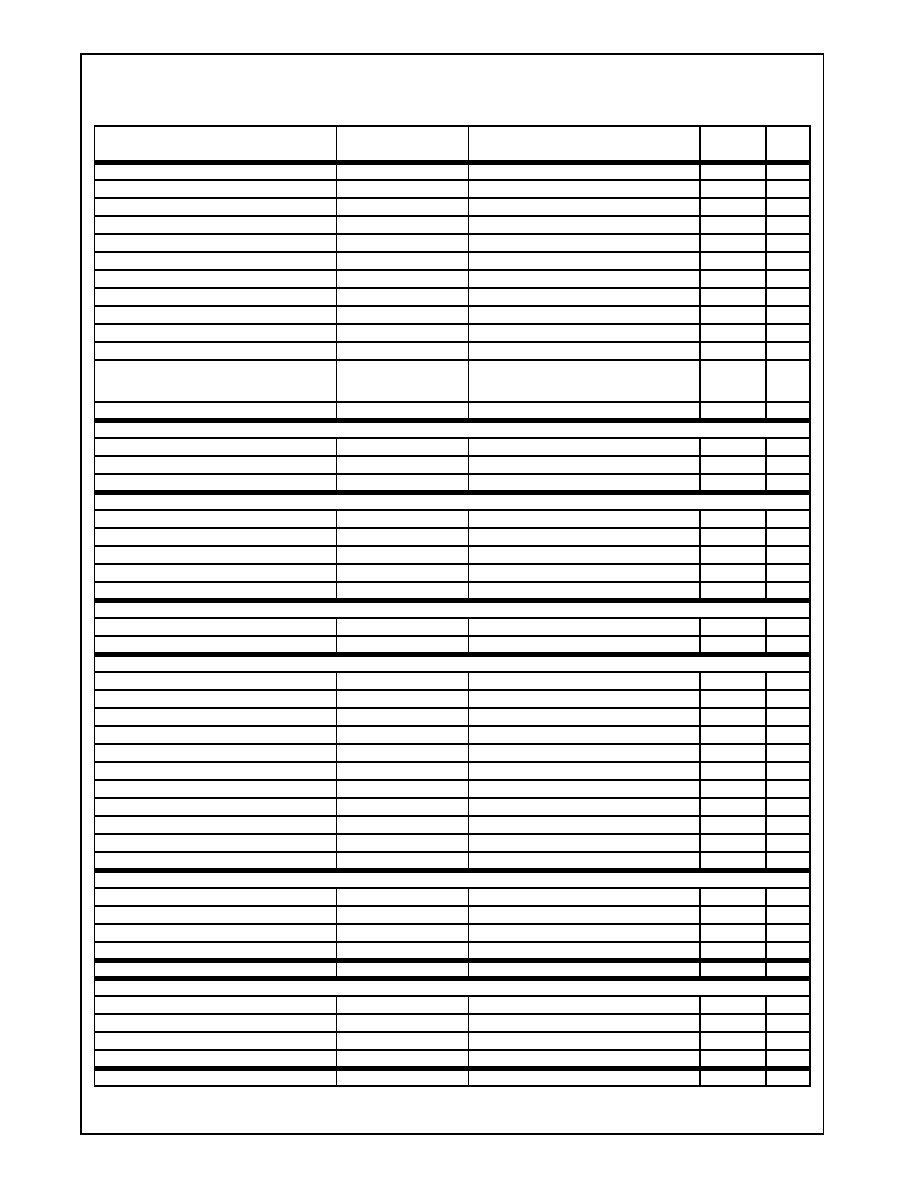
Revision 3.1
227
www.national.com
Instruction Set (
Continued
)
GeodeTM
G
Xm
P
r
ocessor
FNOP No Operation
D9 D0
No Operation
2
FPATAN Function Eval: Tan
-1
(y/x)
D9 F3
ST(1) <--- ATAN[ST(1) / TOS]; then pop TOS
97 - 161
3
FPREM Floating Point Remainder
D9 F8
TOS <--- Rem[TOS / ST(1)]
82 - 91
FPREM1 Floating Point Remainder IEEE
D9 F5
TOS <--- Rem[TOS / ST(1)]
82 - 91
FPTAN Function Eval: Tan(x)
D9 F2
TOS <--- TAN(TOS); then push 1.0 onto stack
117 - 129
1
FRNDINT Round to Integer
D9 FC
TOS <--- Round(TOS)
10 - 20
FRSTOR Load FPU Environment and Register
DD [mod 100 r/m]
Restore state
56 - 72
FSAVE Save FPU Environment and Register
(9B)DD [mod 110 r/m]
Wait, then save state
57 - 67
FNSAVE Save FPU Environment and Register
DD [mod 110 r/m]
Save state
55 - 65
FSCALE Floating Multiply by 2
n
D9 FD
TOS <--- TOS
◊
2
(ST(1))
7 - 14
FSIN Function Evaluation: Sin(x)
D9 FE
TOS <--- SIN(TOS)
76 - 140
1
FSINCOS Function Eval.: Sin(x)& Cos(x)
D9 FB
temp <--- TOS;
TOS <--- SIN(temp); then
push COS(temp) onto stack
145 - 161
1
FSQRT Floating Point Square Root
D9 FA
TOS <--- Square Root of TOS
59 - 60
FST Store FPU Register
Top of Stack
DD [1101 0 n]
ST(n) <--- TOS
2
64-bit Real
DD [mod 010 r/m]
M.DR <--- TOS
2
32-bit Real
D9 [mod 010 r/m]
M.SR <--- TOS
2
FSTP Store FPU Register, Pop
Top of Stack
DB [1101 1 n]
ST(n) <--- TOS; then pop TOS
2
80-bit Real
DB [mod 111 r/m]
M.XR <--- TOS; then pop TOS
2
64-bit Real
DD [mod 011 r/m]
M.DR <--- TOS; then pop TOS
2
32-bit Real
D9 [mod 011 r/m]
M.SR <--- TOS; then pop TOS
2
FBSTP Store BCD Data, Pop
DF [mod 110 r/m]
M.BCD <--- TOS; then pop TOS
57 - 63
FIST Store Integer FPU Register
32-bit Integer
DB [mod 010 r/m]
M.SI <--- TOS
8 - 13
16-bit Integer
DF [mod 010 r/m]
M.WI <--- TOS
7 - 10
FISTP Store Integer FPU Register, Pop
64-bit Integer
DF [mod 111 r/m]
M.LI <--- TOS; then pop TOS
10 - 13
32-bit Integer
DB [mod 011 r/m]
M.SI <--- TOS; then pop TOS
8 - 13
16-bit Integer
DF [mod 011 r/m]
M.WI <--- TOS; then pop TOS
7 - 10
FSTCW Store FPU Mode Control Register
(9B)D9 [mod 111 r/m]
Wait Memory <--- Control Mode Register
5
FNSTCW Store FPU Mode Control Register
D9 [mod 111 r/m]
Memory <--- Control Mode Register
3
FSTENV Store FPU Environment
(9B)D9 [mod 110 r/m]
Wait Memory <--- Env. Registers
14 - 24
FNSTENV Store FPU Environment
D9 [mod 110 r/m]
Memory <--- Env. Registers
12 - 22
FSTSW Store FPU Status Register
(9B)DD [mod 111 r/m]
Wait Memory <--- Status Register
6
FNSTSW Store FPU Status Register
DD [mod 111 r/m]
Memory <--- Status Register
4
FSTSW AX Store FPU Status Register to AX
(9B)DF E0
Wait AX <--- Status Register
4
FNSTSW AX Store FPU Status Register to AX
DF E0
AX <--- Status Register
2
FSUB Floating Point Subtract
Top of Stack
DC [1110 1 n]
ST(n) <--- ST(n) - TOS
4 - 9
80-bit Register
D8 [1110 0 n]
TOS <--- TOS - ST(n
4 - 9
64-bit Real
DC [mod 100 r/m]
TOS <--- TOS - M.DR
4 - 9
32-bit Real
D8 [mod 100 r/m]
TOS <--- TOS - M.SR
4 - 9
FSUBP Floating Point Subtract, Pop
DE [1110 1 n]
ST(n) <--- ST(n) - TOS; then pop TOS
4 - 9
FSUBR Floating Point Subtract Reverse
Top of Stack
DC [1110 0 n]
TOS <--- ST(n) - TOS
4 - 9
80-bit Register
D8 [1110 1 n]
ST(n) <--- TOS - ST(n)
4 - 9
64-bit Real
DC [mod 101 r/m]
TOS <--- M.DR - TOS
4 - 9
32-bit Real
D8 [mod 101 r/m]
TOS <--- M.SR - TOS
4 - 9
FSUBRP Floating Point Subtract Reverse, Pop
DE [1110 0 n]
ST(n) <--- TOS - ST(n); then pop TOS
4 - 9
Table 9-29. FPU Instruction Set Summary (Continued)
FPU Instruction
Opcode
Operation
Clock
Count
Notes
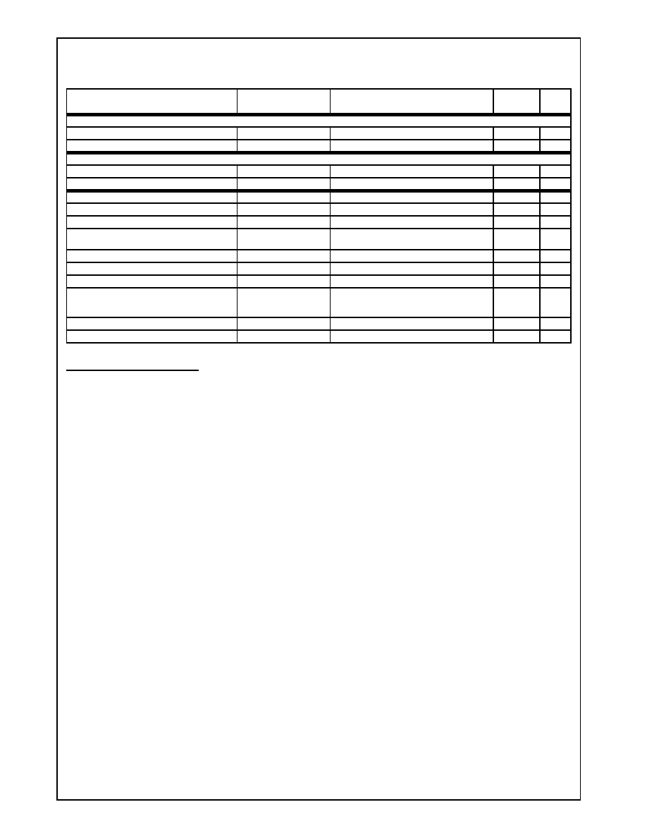
www.national.com
228
Revision 3.1
Instruction Set (
Continued
)
GeodeTM
G
Xm
Pr
ocessor
FPU Instruction Summary Notes
All references to TOS and ST(n) refer to stack layout prior to exe-
cution.
Values popped off the stack are discarded.
A pop from the stack increments the top of stack pointer.
A push to the stack decrements the top of stack pointer.
Notes:
1. For FCOS, FSIN, FSINCOS and FPTAN, time shown is for
absolute value of TOS < 3p/4. Add 90 clock counts for argu-
ment reduction if outside this range.
For FCOS, clock count is 141 if TOS <
/4 and clock count is
92 if
/4 < TOS >
/2.
For FSIN, clock count is 81 to 82 if absolute value of TOS <
/4.
2. For F2XM1, clock count is 92 if absolute value of TOS < 0.5.
3. For FPATAN, clock count is 97 if ST(1)/TOS <
/32.
4. For FYL2XP1, clock count is 170 if TOS is out of range and
regular FYL2X is called.
5. The following opcodes are reserved:
D9D7, D9E2, D9E7, DDFC, DED8, DEDA, DEDC, DEDD,
DEDE, DFFC.
If a reserved opcode is executed, and unpredictable results
may occur (exceptions are not generated).
FISUB Floating Point Integer Subtract
32-bit Integer
DA [mod 100 r/m]
TOS <--- TOS - M.SI
14 - 29
16-bit Integer
DE [mod 100 r/m]
TOS <--- TOS - M.WI
14 - 27
FISUBR Floating Point Integer Subtract Reverse
32-bit Integer Reversed
DA [mod 101 r/m]
TOS <--- M.SI - TOS
14 - 29
16-bit Integer Reversed
DE [mod 101 r/m]
TOS <--- M.WI - TOS
14 - 27
FTST Test Top of Stack
D9 E4
CC set by TOS - 0.0
4
FUCOM Unordered Compare
DD [1110 0 n]
CC set by TOS - ST(n)
4
FUCOMP Unordered Compare, Pop
DD [1110 1 n]
CC set by TOS - ST(n); then pop TOS
4
FUCOMPP Unordered Compare, Pop two
elements
DA E9
CC set by TOS - ST(I); then pop TOS and
ST(1)
4
FWAIT Wait
9B
Wait for FPU not busy
2
FXAM Report Class of Operand
D9 E5
CC <--- Class of TOS
4
FXCH Exchange Register with TOS
D9 [1100 1 n]
TOS <--> ST(n) Exchange
3
FXTRACT Extract Exponent
D9 F4
temp <--- TOS;
TOS <--- exponent (temp); then
push significant (temp) onto stack
11 - 16
FLY2X Function Eval. y
◊
Log2(x)
D9 F1
ST(1) <--- ST(1)
◊
Log
2
(TOS); then pop TOS
145 - 154
FLY2XP1 Function Eval. y
◊
Log2(x+1)
D9 F9
ST(1) <--- ST(1)
◊
Log
2
(1+TOS); then pop TOS
131 - 133
4
Table 9-29. FPU Instruction Set Summary (Continued)
FPU Instruction
Opcode
Operation
Clock
Count
Notes
Revision 3.1
229
www.national.com
Instruction Set (
Continued
)
GeodeTM
G
Xm
P
r
ocessor
9.5
MMX INSTRUCTION SET
The CPU is functionally divided into the FPU unit, and the
integer unit. The FPU has been extended to process both
MMX instructions and floating point instructions in parallel
with the integer unit. Revision 3.1
For example, when the integer unit detects a MMX
instruction, the instruction passes to the FPU unit for exe-
cution. The integer unit continues to execute instructions
while the FPU unit executes the MMX instruction. If
another MMX instruction is encountered, the second
MMX instruction is placed in the MMX queue. Up to four
MMX instructions can be queued.
The MMX instruction set is summarized in Table 9-31 on
page 230. The abbreviations used in the table are listed in
Table 9-30.
Table 9-30. MMX Instruction Set Table Legend
Abbreviation
Description
<----
Result written
[11 mm reg]
Binary or binary groups of digits
mm
One of eight 64-bit MMX registers
reg
A general purpose register
<--sat--
If required, the resultant data is saturated
to remain in the associated data range
<--move--
Source data is moved to result location
[byte]
Eight 8-bit bytes are processed in parallel
[word]
Four 16-bit word are processed in parallel
[dword]
Two 32-bit double words are processed in
parallel
[qword]
One 64-bit quad word is processed
[sign xxx]
The byte, word, double word or quad word
most significant bit is a sign bit
mm1, mm2
MMX Register 1, MMX Register 2
mod r/m
Mod and r/m byte encoding (page 6-6 of
this manual)
pack
Source data is truncated or saturated to
next smaller data size, then concatenated.
packdw
Pack two double words from source and
two double words from destination into four
words in destination register.
packwb
Pack four words from source and four
words from destination into eight bytes in
destination register.
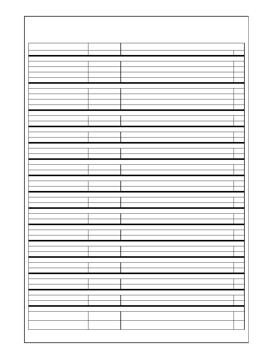
www.national.com
230
Revision 3.1
Instruction Set (
Continued
)
GeodeTM
G
Xm
Pr
ocessor
Table 9-31. MMX Instruction Set Summary
MMX Instructions
Opcode
Operation and Clock Count (Latency/Throughput)
EMMS Empty MMX State
0F77
Tag Word <--- FFFFh (empties the floating point tag word)
1/1
MOVD Move Doubleword
Register to MMX Register
0F6E [11 mm reg]
MMX reg [qword] <--move, zero extend-- reg [dword]
1/1
MMX Register to Register
0F7E [11 mm reg]
reg [qword] <--move-- MMX reg [low dword]
5/1
Memory to MMX Register
0F6E [mod mm r/m]
MMX regr[qword] <--move, zero extend-- memory[dword]
1/1
MMX Register to Memory
0F7E [mod mm r/m]
Memory [dword] <--move-- MMX reg [low dword]
1/1
MOVQ Move Quardword
MMX Register 2 to MMX Register 1
0F6F [11 mm1 mm2]
MMX reg 1 [qword] <--move-- MMX reg 2 [qword]
1/1
MMX Register 1 to MMX Register 2
0F7F [11 mm1 mm2]
MMX reg 2 [qword] <--move-- MMX reg 1 [qword]
1/1
Memory to MMX Register
0F6F [mod mm r/m]
MMX reg [qword] <--move-- memory[qword]
1/1
MMX Register to Memory
0F7F [mod mm r/m]
Memory [qword] <--move-- MMX reg [qword]
1/1
PACKSSDW Pack Dword with Signed Saturation
MMX Register 2 to MMX Register 1
0F6B [11 mm1 mm2]
MMX reg 1 [qword] <--packdw, signed sat-- MMX reg 2, MMX reg 1
1/1
Memory to MMX Register
0F6B [mod mm r/m]
MMX reg [qword] <--packdw, signed sat-- memory, MMX reg
1/1
PACKSSWB Pack Word with Signed Saturation
MMX Register 2 to MMX Register 1
0F63 [11 mm1 mm2]
MMX reg 1 [qword] <--packwb, signed sat-- MMX reg 2, MMX reg 1
1/1
Memory to MMX Register
0F63 [mod mm r/m]
MMX reg [qword] <--packwb, signed sat-- memory, MMX reg
1/1
PACKUSWB Pack Word with Unsigned Saturation
MMX Register 2 to MMX Register 1
0F67 [11 mm1 mm2]
MMX reg 1 [qword] <--packwb, unsigned sat-- MMX reg 2, MMX reg 1
1/1
Memory to MMX Register
0F67 [mod mm r/m]
MMX reg [qword] <--packwb, unsigned sat-- memory, MMX reg
1/1
PADDB Packed Add Byte with Wrap-Around
MMX Register 2 to MMX Register 1
0FFC [11 mm1 mm2] MMX reg 1 [byte] <---- MMX reg 1 [byte] + MMX reg 2 [byte]
1/1
Memory to MMX Register
0FFC [mod mm r/m]
MMX reg[byte] <---- memory [byte] + MMX reg [byte]
1/1
PADDD Packed Add Dword with Wrap-Around
MMX Register 2 to MMX Register 1
0FFE [11 mm1 mm2]
MMX reg 1 [sign dword] <---- MMX reg 1 [sign dword] + MMX reg 2 [sign dword]
1/1
Memory to MMX Register
0FFE [mod mm r/m]
MMX reg [sign dword] <---- memory [sign dword] + MMX reg [sign dword]
1/1
PADDSB Packed Add Signed Byte with Saturation
MMX Register 2 to MMX Register 1
0FEC [11 mm1 mm2] MMX reg 1 [sign byte] <--sat-- MMX reg 1 [sign byte] + MMX reg 2 [sign byte]
1/1
Memory to Register
0FEC [mod mm r/m]
MMX reg [sign byte] <--sat-- memory [sign byte] + MMX reg [sign byte]
1/1
PADDSW Packed Add Signed Word with Saturation
MMX Register 2 to MMX Register 1
0FED [11 mm1 mm2] MMX reg 1 [sign word] <--sat-- MMX reg 1 [sign word] + MMX reg 2 [sign word]
1/1
Memory to Register
0FED [mod mm r/m]
MMX reg [sign word] <--sat-- memory [sign word] + MMX reg [sign word]
1/1
PADDUSB Add Unsigned Byte with Saturation
MMX Register 2 to MMX Register 1
0FDC [11 mm1 mm2] MMX reg 1 [byte] <--sat-- MMX reg 1 [byte] + MMX reg 2 [byte]
1/1
Memory to Register
0FDC [mod mm r/m]
MMX reg [byte] <--sat-- memory [byte] + MMX reg [byte]
1/1
PADDUSW Add Unsigned Word with Saturation
MMX Register 2 to MMX Register 1
0FDD [11 mm1 mm2] MMX reg 1 [word] <--sat-- MMX reg 1 [word] + MMX reg 2 [word]
1/1
Memory to Register
0FDD [mod mm r/m]
MMX reg [word] <--sat-- memory [word] + MMX reg [word]
1/1
PADDW Packed Add Word with Wrap-Around
MMX Register 2 to MMX Register 1
0FFD [11 mm1 mm2] MMX reg 1 [word] <---- MMX reg 1 [word] + MMX reg 2 [word]
1/1
Memory to MMX Register
0FFD [mod mm r/m]
MMX reg [word] <---- memory [word] + MMX reg [word]
1/1
PAND Bitwise Logical AND
MMX Register 2 to MMX Register 1
0FDB [11 mm1 mm2] MMX reg 1 [qword] <--logic AND-- MMX reg 1 [qword], MMX reg 2 [qword]
1/1
Memory to MMX Register
0FDB [mod mm r/m]
MMX reg [qword] <--logic AND-- memory [qword], MMX reg [qword]
PANDN Bitwise Logical AND NOT
MMX Register 2 to MMX Register 1
0FDF [11 mm1 mm2] MMX reg 1 [qword] <--logic AND -- NOT MMX reg 1 [qword], MMX reg 2 [qword]
1/1
Memory to MMX Register
0FDF [mod mm r/m]
MMX reg [qword] <--logic AND-- NOT MMX reg [qword], Memory [qword]
1/1
PCMPEQB Packed Byte Compare for Equality
MMX Register 2 with MMX Register 1 0F74 [11 mm1 mm2]
MMX reg 1 [byte] <--FFh-- if MMX reg 1 [byte] = MMX reg 2 [byte]
MMX reg 1 [byte]<--00h-- if MMX reg 1 [byte] NOT = MMX reg 2 [byte]
1/1
Memory with MMX Register
0F74 [mod mm r/m]
MMX reg [byte] <--FFh-- if memory[byte] = MMX reg [byte]
MMX reg [byte] <--00h-- if memory[byte] NOT = MMX reg [byte]
1/1
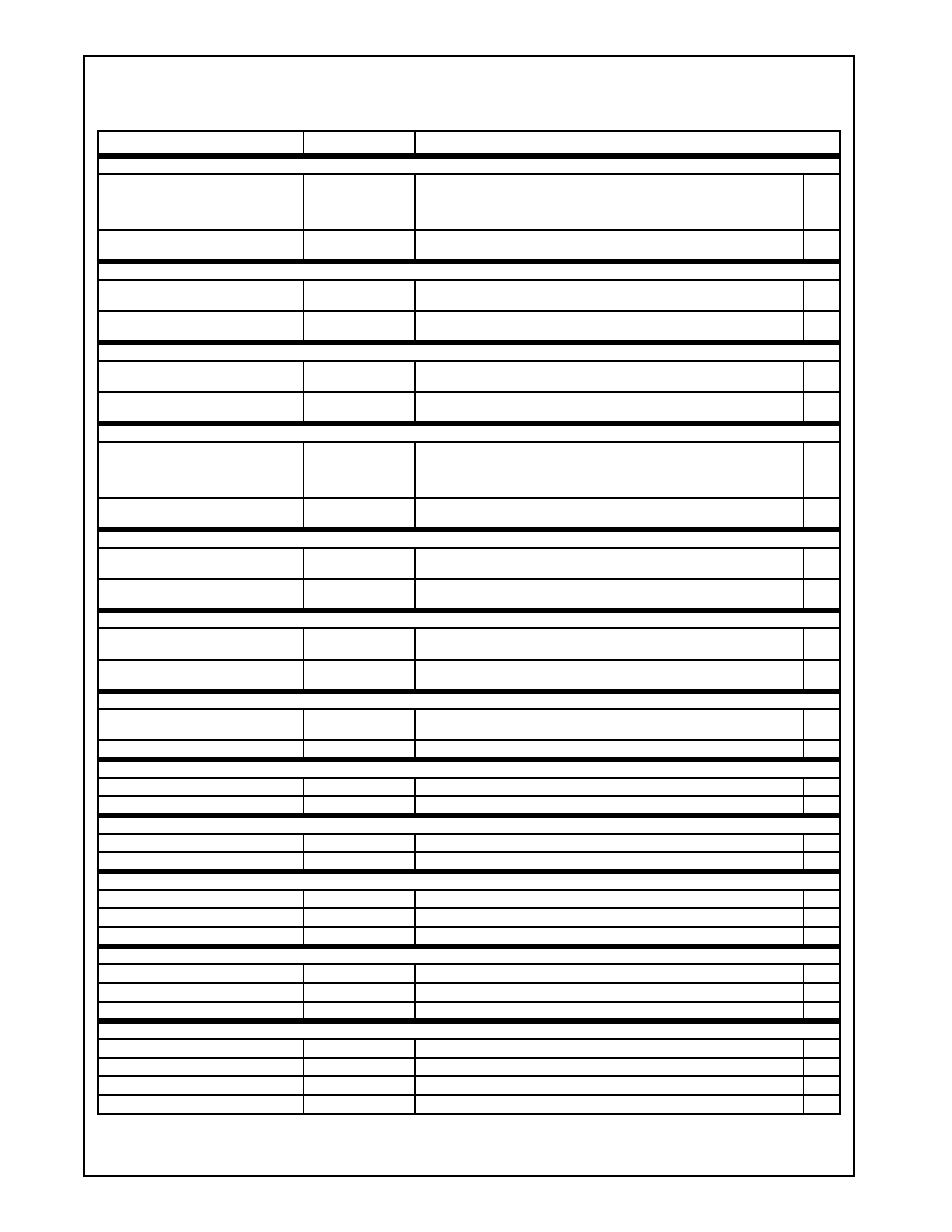
Revision 3.1
231
www.national.com
Instruction Set (
Continued
)
GeodeTM
G
Xm
P
r
ocessor
PCMPEQD Packed Dword Compare for Equality
MMX Register 2 with MMX Register 1 0F76 [11 mm1 mm2]
MMX reg 1 [dword] <--FFFF FFFFh-- if MMX reg 1 [dword] = MMX reg 2
[dword]
MMX reg 1 [dword]<--0000 0000h--if MMX reg 1[dword] NOT = MMX reg 2
[dword]
1/1
Memory with MMX Register
0F76 [mod mm r/m]
MMX reg [dword] <--FFFF FFFFh-- if memory[dword] = MMX reg [dword]
MMX reg [dword] <--0000 0000h-- if memory[dword] NOT = MMX reg [dword]
1/1
PCMPEQW Packed Word Compare for Equality
MMX Register 2 with MMX Register 1 0F75 [11 mm1 mm2]
MMX reg 1 [word] <--FFFFh-- if MMX reg 1 [word] = MMX reg 2 [word]
MMX reg 1 [word]<--0000h-- if MMX reg 1 [word] NOT = MMX reg 2 [word]
1/1
Memory with MMX Register
0F75 [mod mm r/m]
MMX reg [word] <--FFFFh-- if memory[word] = MMX reg [word]
MMX reg [word] <--0000h-- if memory[word] NOT = MMX reg [word]
1/1
PCMPGTB Pack Compare Greater Than Byte
MMX Register 2 to MMX Register 1
0F64 [11 mm1 mm2]
MMX reg 1 [byte] <--FFh-- if MMX reg 1 [byte] > MMX reg 2 [byte]
MMX reg 1 [byte]<--00h-- if MMX reg 1 [byte] NOT > MMX reg 2 [byte]
1/1
Memory with MMX Register
0F64 [mod mm r/m]
MMX reg [byte] <--FFh-- if memory[byte] > MMX reg [byte]
MMX reg [byte] <--00h-- if memory[byte] NOT > MMX reg [byte]
1/1
PCMPGTD Pack Compare Greater Than Dword
MMX Register 2 to MMX Register 1
0F66 [11 mm1 mm2]
MMX reg 1 [dword] <--FFFF FFFFh-- if MMX reg 1 [dword] > MMX reg 2
[dword]
MMX reg 1 [dword]<--0000 0000h--if MMX reg 1 [dword]NOT > MMX reg 2
[dword]
1/1
Memory with MMX Register
0F66 [mod mm r/m]
MMX reg [dword] <--FFFF FFFFh-- if memory[dword] > MMX reg [dword]
MMX reg [dword] <--0000 0000h-- if memory[dword] NOT > MMX reg [dword]
1/1
PCMPGTW Pack Compare Greater Than Word
MMX Register 2 to MMX Register 1
0F65 [11 mm1 mm2]
MMX reg 1 [word] <--FFFFh-- if MMX reg 1 [word] > MMX reg 2 [word]
MMX reg 1 [word]<--0000h-- if MMX reg 1 [word] NOT > MMX reg 2 [word]
1/1
Memory with MMX Register
0F65 [mod mm r/m]
MMX reg [word] <--FFFFh-- if memory[word] > MMX reg [word]
MMX reg [word] <--0000h-- if memory[word] NOT > MMX reg [word]
1/1
PMADDWD Packed Multiply and Add
MMX Register 2 to MMX Register 1
0FF5 [11 mm1 mm2]
MMX reg 1 [dword] <--add-- [dword]<---- MMX reg 1 [sign word]*MMX reg
2[sign word]
2/1
Memory to MMX Register
0FF5 [mod mm r/m]
MMX reg 1 [dword] <--add-- [dword] <---- memory [sign word] * Memory [sign
word]
2/1
PMULHW Packed Multiply High
MMX Register 2 to MMX Register 1
0FE5 [11 mm1 mm2]
MMX reg 1 [word] <--upper bits-- MMX reg 1 [sign word] * MMX reg 2 [sign
word]
2/1
Memory to MMX Register
0FE5 [mod mm r/m]
MMX reg 1 [word] <--upper bits-- memory [sign word] * Memory [sign word]
2/1
PMULLW Packed Multiply Low
MMX Register 2 to MMX Register 1
0FD5 [11 mm1 mm2]
MMX reg 1 [word] <--lower bits-- MMX reg 1 [sign word] * MMX reg 2 [sign word]
2/1
Memory to MMX Register
0FD5 [mod mm r/m]
MMX reg 1 [word] <--lower bits-- memory [sign word] * Memory [sign word]
2/1
POR Bitwise OR
MMX Register 2 to MMX Register 1
0FEB [11 mm1 mm2] MMX reg 1 [qword] <--logic OR-- MMX reg 1 [qword], MMX reg 2 [qword]
1/1
Memory to MMX Register
0FEB [mod mm r/m]
MMX reg [qword] <--logic OR-- MMX reg [qword], memory[qword]
1/1
PSLLD Packed Shift Left Logical Dword
MMX Register 1 by MMX Register 2
0FF2 [11 mm1 mm2]
MMX reg 1 [dword] <--shift left, shifting in zeroes by MMX reg 2 [dword]--
1/1
MMX Register by Memory
0FF2 [mod mm r/m]
MMX reg [dword] <--shift left, shifting in zeroes by memory[dword]--
1/1
MMX Register by Immediate
0F72 [11 110 mm] #
MMX reg [dword] <--shift left, shifting in zeroes by [im byte]--
1/1
PSLLQ Packed Shift Left Logical Qword
MMX Register 1 by MMX Register 2
0FF3 [11 mm1 mm2]
MMX reg 1 [qword] <--shift left, shifting in zeroes by MMX reg 2 [qword]--
1/1
MMX Register by Memory
0FF3 [mod mm r/m]
MMX reg [qword] <--shift left, shifting in zeroes by [qword]--
1/1
MMX Register by Immediate
0F73 [11 110 mm] #
MMX reg [qword] <--shift left, shifting in zeroes by [im byte]--
1/1
PSLLW Packed Shift Left Logical Word
MMX Register 1 by MMX Register 2
0FF1 [11 mm1 mm2]
MMX reg 1 [word] <--shift left, shifting in zeroes by MMX reg 2 [word]--
1/1
MMX Register by Memory
0FF1 [mod mm r/m]
MMX reg [word] <--shift left, shifting in zeroes by memory[word]--
1/1
MMX Register by Immediate
0F71 [11 110mm] #
MMX reg [word] <--shift left, shifting in zeroes by [im byte]--
1/1
Table 9-31. MMX Instruction Set Summary (Continued)
MMX Instructions
Opcode
Operation and Clock Count (Latency/Throughput)

www.national.com
232
Revision 3.1
Instruction Set (
Continued
)
GeodeTM
G
Xm
Pr
ocessor
PSRAD Packed Shift Right Arithmetic Dword
MMX Register 1 by MMX Register 2
0FE2 [11 mm1 mm2]
MMX reg 1 [dword] <--arith shift right, shifting in zeroes by MMX reg 2 [dword--]
1/1
MMX Register by Memory
0FE2 [mod mm r/m]
MMX reg [dword] <--arith shift right, shifting in zeroes by memory[dword]--
1/1
MMX Register by Immediate
0F72 [11 100 mm] #
MMX reg [dword] <--arith shift right, shifting in zeroes by [im byte]--
1/1
PSRAW Packed Shift Right Arithmetic Word
MMX Register 1 by MMX Register 2
0FE1 [11 mm1 mm2]
MMX reg 1 [word] <--arith shift right, shifting in zeroes by MMX reg 2 [word]--
1/1
MMX Register by Memory
0FE1 [mod mm r/m]
MMX reg [word] <--arith shift right, shifting in zeroes by memory[word--]
1/1
MMX Register by Immediate
0F71 [11 100 mm] #
MMX reg [word] <--arith shift right, shifting in zeroes by [im byte]--
1/1
PSRLD Packed Shift Right Logical Dword
MMX Register 1 by MMX Register 2
0FD2 [11 mm1 mm2]
MMX reg 1 [dword] <--shift right, shifting in zeroes by MMX reg 2 [dword]--
1/1
MMX Register by Memory
0FD2 [mod mm r/m]
MMX reg [dword] <--shift right, shifting in zeroes by memory[dword]--
1/1
MMX Register by Immediate
0F72 [11 010 mm] #
MMX reg [dword] <--shift right, shifting in zeroes by [im byte]--
1/1
PSRLQ Packed Shift Right Logical Qword
MMX Register 1 by MMX Register 2
0FD3 [11 mm1 mm2]
MMX reg 1 [qword] <--shift right, shifting in zeroes by MMX reg 2 [qword]
1/1
MMX Register by Memory
0FD3 [mod mm r/m]
MMX reg [qword] <--shift right, shifting in zeroes by memory[qword]
1/1
MMX Register by Immediate
0F73 [11 010 mm] #
MMX reg [qword] <--shift right, shifting in zeroes by [im byte]
1/1
PSRLW Packed Shift Right Logical Word
MMX Register 1 by MMX Register 2
0FD1 [11 mm1 mm2]
MMX reg 1 [word] <--shift right, shifting in zeroes by MMX reg 2 [word]
1/1
MMX Register by Memory
0FD1 [mod mm r/m]
MMX reg [word] <--shift right, shifting in zeroes by memory[word]
1/1
MMX Register by Immediate
0F71 [11 010 mm] #
MMX reg [word] <--shift right, shifting in zeroes by imm[word]
1/1
PSUBB Subtract Byte With Wrap-Around
MMX Register 2 to MMX Register 1
0FF8 [11 mm1 mm2]
MMX reg 1 [byte] <---- MMX reg 1 [byte] subtract MMX reg 2 [byte]
1/1
Memory to MMX Register
0FF8 [mod mm r/m]
MMX reg [byte] <---- MMX reg [byte] subtract memory [byte]
1/1
PSUBD Subtract Dword With Wrap-Around
MMX Register 2 to MMX Register 1
0FFA [11 mm1 mm2]
MMX reg 1 [dword] <---- MMX reg 1 [dword] subtract MMX reg 2 [dword]
1/1
Memory to MMX Register
0FFA [mod mm r/m]
MMX reg [dword] <---- MMX reg [dword] subtract memory [dword]
1/1
PSUBSB Subtract Byte Signed With Saturation
MMX Register 2 to MMX Register 1
0FE8 [11 mm1 mm2]
MMX reg 1 [sign byte] <--sat-- MMX reg 1 [sign byte] subtract MMX reg 2 [sign
byte]
1/1
Memory to MMX Register
0FE8 [mod mm r/m]
MMX reg [sign byte] <--sat-- MMX reg [sign byte] subtract memory [sign byte]
1/1
PSUBSW Subtract Word Signed With Saturation
MMX Register 2 to MMX Register 1
0FE9 [11 mm1 mm2]
MMX reg 1 [sign word] <--sat-- MMX reg 1 [sign word] subtract MMX reg 2 [sign
word]
1/1
Memory to MMX Register
0FE9 [mod mm r/m]
MMX reg [sign word] <--sat-- MMX reg [sign word] subtract memory [sign word]
1/1
PSUBUSB Subtract Byte Unsigned With Saturation
MMX Register 2 to MMX Register 1
0FD8 [11 mm1 mm2]
MMX reg 1 [byte] <--sat-- MMX reg 1 [byte] subtract MMX reg 2 [byte]
1/1
Memory to MMX Register
0FD8 [11 mm reg]
MMX reg [byte] <--sat-- MMX reg [byte] subtract memory [byte]
1/1
PSUBUSW Subtract Word Unsigned With Saturation
MMX Register 2 to MMX Register 1
0FD9 [11 mm1 mm2]
MMX reg 1 [word] <--sat-- MMX reg 1 [word] subtract MMX reg 2 [word]
1/1
Memory to MMX Register
0FD9 [11 mm reg]
MMX reg [word] <--sat-- MMX reg [word] subtract memory [word]
1/1
PSUBW Subtract Word With Wrap-Around
MMX Register 2 to MMX Register 1
0FF9 [11 mm1 mm2]
MMX reg 1 [word] <---- MMX reg 1 [word] subtract MMX reg 2 [word]
1/1
Memory to MMX Register
0FF9 [mod mm r/m]
MMX reg [word] <---- MMX reg [word] subtract memory [word]
1/1
PUNPCKHBW Unpack High Packed Byte, Data to Packed Words
MMX Register 2 to MMX Register 1
0F68 [11 mm1 mm2]
MMX reg 1 [byte] <--interleave-- MMX reg 1 [up byte], MMX reg 2 [up byte]
1/1
Memory to MMX Register
0F68 [11 mm reg]
MMX reg [byte] <--interleave-- memory [up byte], MMX reg [up byte]
1/1
PUNPCKHDQ Unpack High Packed Dword, Data to Qword
MMX Register 2 to MMX Register 1
0F6A [11 mm1 mm2]
MMX reg 1 [dword] <--interleave-- MMX reg 1 [up dword], MMX reg 2 [up
dword]
1/1
Memory to MMX Register
0F6A [11 mm reg]
MMX reg [dword] <--interleave-- memory [up dword], MMX reg [up dword]
1/1
PUNPCKHWD Unpack High Packed Word, Data to Packed Dwords
MMX Register 2 to MMX Register 1
0F69 [11 mm1 mm2]
MMX reg 1 [word] <--interleave-- MMX reg 1 [up word], MMX reg 2 [up word]
1/1
Memory to MMX Register
0F69 [11 mm reg]
MMX reg [word] <--interleave-- memory [up word], MMX reg [up word]
1/1
Table 9-31. MMX Instruction Set Summary (Continued)
MMX Instructions
Opcode
Operation and Clock Count (Latency/Throughput)
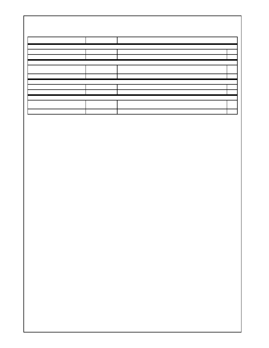
Revision 3.1
233
www.national.com
Instruction Set (
Continued
)
GeodeTM
G
Xm
P
r
ocessor
PUNPCKLBW Unpack Low Packed Byte, Data to Packed Words
MMX Register 2 to MMX Register 1
0F60 [11 mm1 mm2]
MMX reg 1 [word] <--interleave-- MMX reg 1 [low byte], MMX reg 2 [low byte]
1/1
Memory to MMX Register
0F60 [11 mm reg]
MMX reg [word] <--interleave-- memory [low byte], MMX reg [low byte]
1/1
PUNPCKLDQ Unpack Low Packed Dword, Data to Qword
MMX Register 2 to MMX Register 1
0F62 [11 mm1 mm2]
MMX reg 1 [word] <--interleave-- MMX reg 1 [low dword], MMX reg 2 [low
dword]
1/1
Memory to MMX Register
0F62 [11 mm reg]
MMX reg [word] <--interleave-- memory [low dword], MMX reg [low dword]
1/1
PUNPCKLWD Unpack Low Packed Word, Data to Packed Dwords
MMX Register 2 to MMX Register 1
0F61 [11 mm1 mm2]
MMX reg 1 [word] <--interleave-- MMX reg 1 [low word], MMX reg 2 [low word]
1/1
Memory to MMX Register
0F61 [11 mm reg]
MMX reg [word] <--interleave-- memory [low word], MMX reg [low word]
1/1
PXOR Bitwise XOR
MMX Register 2 to MMX Register 1
0FEF [11 mm1 mm2]
MMX reg 1 [qword] <--logic exclusive OR-- MMX reg 1 [qword], MMX reg 2
[qword]
1/1
Memory to MMX Register
0FEF [11 mm reg]
MMX reg [qword] <--logic exclusive OR-- memory[qword], MMX reg [qword]
1/1
Table 9-31. MMX Instruction Set Summary (Continued)
MMX Instructions
Opcode
Operation and Clock Count (Latency/Throughput)
www.national.com
234
Revision 3.1
Instruction Set (
Continued
)
GeodeTM
G
Xm
Pr
ocessor
9.6
NATIONAL SEMICONDUCTOR EXTENDED MMX INSTRUCTION SET
National Semiconductor has added instructions to its
implementation of the MMX Architecture in order to facili-
tate writing of multimedia applications. In general, these
instructions allow more efficient implementation of multi-
media algorithms, or more precision in computation than
can be achieved using the basic set of MMX instructions.
All of the added instructions follow the SIMD (single
instruction, multiple data) format. Many of the instructions
add flexibility to the MMX architecture by allowing both
source operands of an instruction to be preserved, while
the result goes to a separate register that is derived from
the input.
Table 9-33 on page 235 summarizes the Extended MMX
Instructions. The abbreviations used in the table are listed
in Table 9-32.
Configuration control register CCR7(0) at location EBh
must be set to allow the execution of the Extended MMX
instructions.
Table 9-32. Extend MMX Instruction Set Table
Legend
Abbreviation
Description
<----
Result written
[11 mm reg]
Binary or binary groups of digits
mm
One of eight 64-bit MMX registers
reg
A general purpose register
<--sat--
If required, the resultant data is saturated
to remain in the associated data range
<--move--
Source data is moved to result location
[byte]
Eight 8-bit bytes are processed in parallel
[word]
Four 16-bit WORD are processed in paral-
lel
[dword]
Two 32-bit DWORDs are processed in par-
allel
[qword]
One 64-bit QWORD is processed
[sign xxx]
The BYTE, WORD, DWORD or QWORD
most significant bit is a sign bit
mm1, mm2
MMX Register 1, MMX Register 2
mod r/m
Mod and r/m byte encoding (page 6-6 of
this manual)
pack
Source data is truncated or saturated to
next smaller data size, then concatenated.
packdw
Pack two DWORDs from source and two
DWORDs from destination into four
WORDs in destination register.
packwb
Pack four WORDs from source and four
WORDs from destination into eight BYTEs
in destination register.
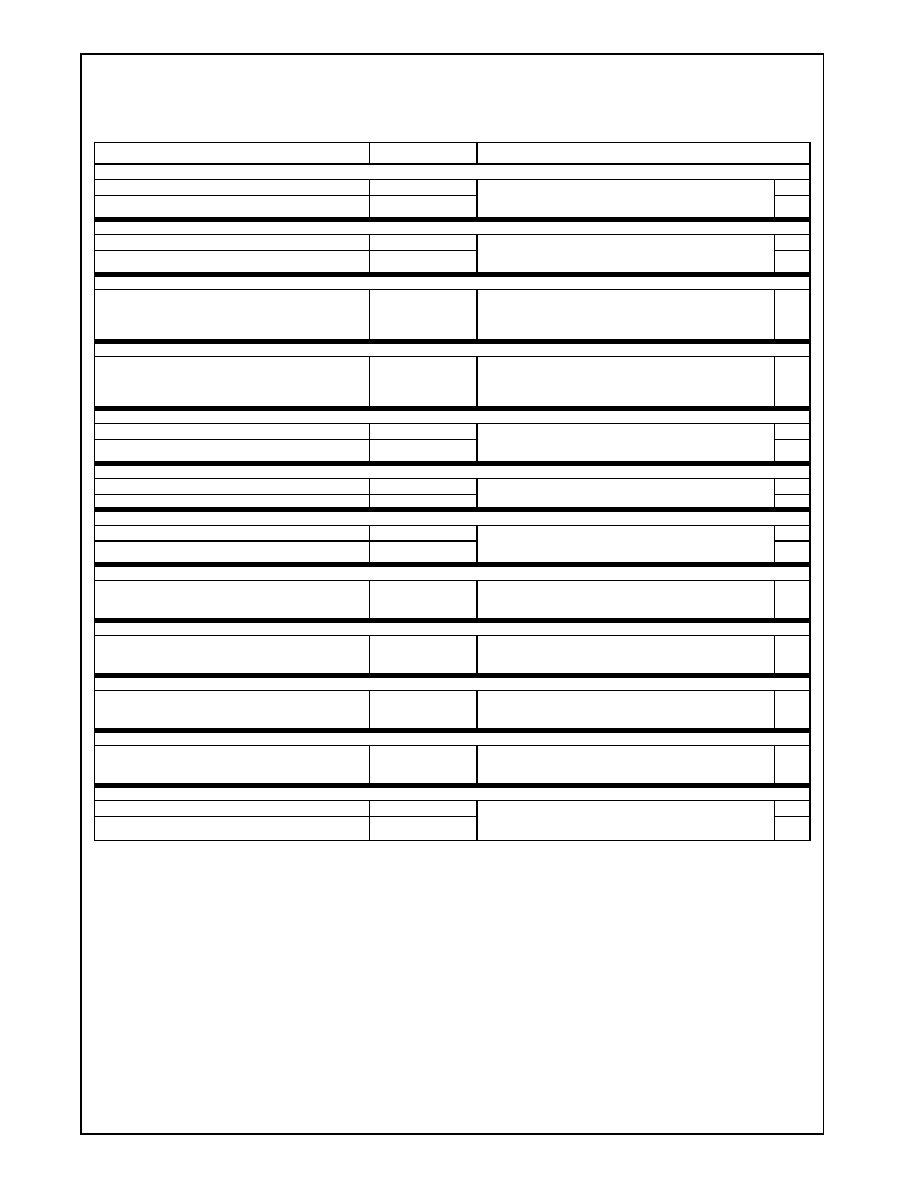
Revision 3.1
235
www.national.com
Instruction Set (
Continued
)
GeodeTM
G
Xm
P
r
ocessor
Table 9-33. Extended MMX Instruction Set Summary
MMX Instructions
Opcode
Operation and Clock Count
PADDSIW Packed Add Signed Word with Saturation Using Implied Destination
MMX Register plus MMX Register to Implied Register
0F51 [11 mm1 mm2]
Sum signed packed word from MMX register/memory --->
signed packed word in MMX register, saturate, and write result
---> implied register
1
Memory plus MMX Register to Implied Register
0F51 [mod mm r/m]
1
PAVEB Packed Average Byte
MMX Register 2 with MMX Register 1
0F50 [11 mm1 mm2]
Average packed byte from the MMX register/memory with
packed byte in the MMX register. Result is placed in the MMX
register.
1
Memory with MMX Register
0F50 [mod mm r/m]
1
PDISTIB Packed Distance and Accumulate with Implied Register
Memory, MMX Register to Implied Register
0F54 [mod mm r/m]
Find absolute value of difference between packed byte in
memory and packed byte in the MMX register. Using unsigned
saturation, accumulate with value in implied destination regis-
ter.
2
PMACHRIW Packed Multiply and Accumulate with Rounding
Memory to MMX Register
0F5E[mod mm r/m]
Multiply the packed word in the MMX register by the packed
word in memory. Sum the 32-bit results pairwise. Accumulate
the result with the packed signed word in the implied destina-
tion register.
2
PMAGW Packed Magnitude
MMX Register 2 to MMX Register 1
0F52 [11 mm1 mm2]
Set the destination equal ---> the packed word with the largest
magnitude, between the packed word in the MMX regis-
ter/memory and the MMX register.
2
Memory to MMX Register
0F52 [mod mm r/m]
2
PMULHRIW Packed Multiply High with Rounding, Implied Destination
MMX Register 2 to MMX Register1
0F5D [11 mm1 mm2]
Packed multiply high with rounding and store bits 30 - 15 in
implied register.
2
Memory to MMX Register
0F5D [mod mm r/m]
2
PMULHRW Packed Multiply High with Rounding
MMX Register 2 to MMX Register 1
0F59 [11 mm1 mm2]
Multiply the signed packed word in the MMX register/memory
with the signed packed word in the MMX register. Round with
1/2 bit 15, and store bits 30 - 15 of result in the MMX register.
2
Memory to MMX Register
0F59 [mod mm r/m]
2
PMVGEZB Packed Conditional Move If Greater Than or Equal to Zero
Memory to MMX Register
0F5C [mod mm r/m]
Conditionally move packed byte from memory ---> packed byte
in the MMX register if packed byte in implied MMX register is
greater than or equal ---> zero.
1
PMVLZB Packed Conditional Move If Less Than Zero
Memory to MMX Register
0F5B [mod mm r/m]
Conditionally move packed byte from memory ---> packed byte
in the MMX register if packed byte in implied MMX register is
less than zero.
1
PMVNZB Packed Conditional Move If Not Zero
Memory to MMX Register
0F5A [mod mm r/m]
Conditionally move packed byte from memory ---> packed byte
in the MMX register if packed byte in implied MMX register is
not zero.
1
PMVZB Packed Conditional Move If Zero
Memory to MMX Register
0F58 [mod mm r/m]
Conditionally move packed byte from memory ---> packed byte
in the MMX register if packed byte in implied the MMX register
is zero.
1
PSUBSIW Packed Subtracted with Saturation Using Implied Destination
MMX Register 2 to MMX Register 1
0F55 [11 mm1 mm2]
Subtract signed packed word in the MMX register/memory from
signed packed word in the MMX register, saturate, and write
result ---> implied register.
1
Memory to MMX Register
0F55 [mod mm r/m]
1

www.national.com
236
Revision 3.1
GeodeTM
G
Xm
Pr
ocessor
Appendix A
Support Documentation
A.1
ORDER INFORMATION
A.2
DATA BOOK REVISION HISTORY
This document is a report of the revision/creation process
of the data book for the GXm processor. Any revisions
(i.e., additions, deletions, parameter corrections, etc.) are
recorded in the tables below.
Order Number
Part Marking
Core
Frequency (MHz)
Temperature
(Degree C)
Package
30070-53
GXm-266P 2.9V 70C
266
70
SPGA
30071-53
GXm-266P 2.9V 85C
266
85
SPGA
30170-53
GXm-266B 2.9V 70C
266
70
BGA
30171-53
GXm-266B 2.9V 85C
266
85
BGA
30050-33
GXm-233P 2.9V 70C
233
70
SPGA
30054-33
GXm-233P 2.9V 85C
233
85
SPGA
30150-33
GXm-233B 2.9V 70C
233
70
BGA
30151-33
GXm-233B 2.9V 85C
233
85
BGA
30040-23
GXm-200P 2.9V 70C
200
70
SPGA
30044-23
GXm-200P 2.9V 85C
200
85
SPGA
30140-23
GXm-200B 2.9V 70C
200
70
BGA
30141-23
GXm-200B 2.9V 85C
200
85
BGA
30030-23
GXm-180P 2.9V 70C
180
70
SPGA
30034-23
GXm-180P 2.9V 85C
180
85
SPGA
30130-23
GXm-180B 2.9V 70C
180
70
BGA
30131-23
GXm-180B 2.9V 85C
180
85
BGA
Table A-1. Revision History
Revision #
(PDF Date)
Revisions / Comments
0.0 (2/5/98)
Creation phase
0.1 (2/25/98)
Creation phase continues - added functional description.
0.2 (3/24/98)
Creation phase continues - added 233 MHz parameters.
0.3 (4/22/98)
Creation phase continues - added 266 MHz numbers.
1.0 (8/13/98)
All sections complete - added 300 MHz numbers, added Index.
2.0 (10/29/98)
Major change is new values for 352 BGA Mechanical.
3.0 (9/21/99)
Converted to National Semiconductor format and updated for addendum revision 3.0.
3.1 (4/6/00)
Formatting changes and one change from engineering. See Table A-2 for details.
Table A-2. Edits to Current Revision
Section
Revision
3.0 Processor
Programming
∑ Combined bits 1 and 2 of Configuration Control Register 1 in Table 3-11 on page 52.
7.0 Electricals
∑ All references to Recommended Operating Conditions became Operating Conditions.
∑ Table 7-3 on page 183 - Changed supply voltage from 3.6V to 3.2V.

Revision 3.1
237
www.national.com
Index
GeodeTM
G
Xm
P
r
ocessor
A
Absolute Maximum Ratings
183
AC Characteristics
186
Accessing
157
Address Spaces
60
Directory Table Entry (DTE)
73
DTE Cache
73
I/O Address Space
60
Memory Address Space
60
Memory Addressing Modes
61
Offset Mechanism
61
Page Frame Offset (PFO)
73
Page Table Entry (PTE)
73
Paging Mechanism
72
Translation Look-Aside Buffer
74
Address Translation
108
Application Register Set
40
B
BGA Ball Assignments by Ball Number
15
BGA Ball Assignments by Pin Name
17
BGA Ball Assignments Diagram
14
C
Cache
BB0_BASE
95
BB0_POINTER
95
BB1_BASE
95
BB1_POINTER
95
GCR register (Index B8h)
95
L1 cache
95
scratchpad memory
95
Write-back caching
95
Cache Controller
95
Cache Disable, bit 30
95
Cache Test Operations
58
call gate
69
Current Privilege Level
69
Descriptor Privilege Level
69
Descriptor Privilege Level in Destination
69
Descriptors Bit Definitions
69
Segment Selector Field
69
CCR1
System Management Memory Access
49
CCR1 Configuration Control Register 1 Index C1h
49
CCR2
Enable Suspend Pins
49
Lock NW Bit
49
Suspend on HALT
49
Write-Through Region 1
49
CCR2 Configuration Control Register 2 Index C2h
49
CCR3
Load/Store Serialize 1 GByte to 2 GBytes
49
Load/Store Serialize 2 GBytes to 3 GBytes
49
Load/Store Serialize 3 GBytes to 4 GBytes
49
Map Enable
49
NMI Enable
49
SMM Register Lock
49
CCR3 Configuration Control Register 3 Index C3h
49
CCR4
Directory Table Entry Cache
50
Enable CPUID Instruction
50
I/O Recovery Time
50
Memory Read Bypassing
50
SMI Nest
50
CCR4 Configuration Control Register 4 Index E8h
50
CCR7
Cyrix Extended MMX Instructions Enable
50
NMI Enabl
50
CCR7 Configuration Control Register 7 Index EBh
50
Clock Mode
24
Configuration Register Map
48
Control Registers
48
Device ID Registers
48
Graphics/VGA Related Registers
48
SMM Base Header Address Registers
48
Configuration Register Summary
47
Conforming Code Segments
69
Control Transfer
87
CPU_READ
99
CPU_READ/WRITE
EAX instructions
99
EBX instructions
99
CPU_WRITE
99
CPUID Instruction
208
EAX = 0000 0000h
208
EAX = 0000 0001h
208
EAX = 0000 0002h
209
EAX = 8000 0000h
210
EAX = 8000 0001h
210
EAX = 8000 0002h
211
EAX = 8000 0003h
211
EAX = 8000 0004h
211
EAX = 8000 0005h
211
CPUID Levels
208
CPUID Levels, Extended
210
CR0 Register
45
Alignment Check Mask
46
Cache Disable
46
Emulate Processor Extension
46
Monitor Processor Extension
46
Not Write-Through
46
Numerics Exception
46
Paging Enable Bit
45
Protected Mode Enable
46
Task Switched
46
Write Protect
46
CR2 Register
45
Page Fault Linear Address
45
CR3 Register
45
Page Directory Base Register
45
CR4 Register
45
Time Stamp Counter Instruction
45
D
DC Characteristics
185
Descriptor Bit Structure
67
Descriptor Types
87
Descriptors
Gate
67
gate
69
Interrupt
67
Task
67
Device Select
28
DEVSEL
28
DIMM
112
DIR0
Device ID
51
DIR0 Device Identification Register 0 Index FEh
51
DIR1
Device Identification Revision
51
DIR1 Device Identification Register 1 Index FFh
51

www.national.com
238
Revision 3.1
Index (
Continued
)
GeodeTM
G
Xm
Pr
ocessor
Directory Table Entry
73
Display Controller
129
≠
154
Buffer Organization
135
CODEC hardware
129
Compression Logic
130
Compression Technology
130
CRT Display Modes
134
Cursor Pattern Memory
136
DC Memory Organization
135
DC_CURSOR_COLOR Register (BX_BASE+8360h) 131
Display FIFO
130
Display Modes
131
Display Timing
131
Dither/Frame-Rate Modulation (FRM)
131
Graphics Memory Map
135
Hardware Cursor
131
Memory Management
130
Pixel Arrangement Within a DWORD
135
RAMDAC
129
TFT LCD flat panel
129
TFT Panel Data Bus Formats
133
TFT Panel Display Modes
132
VESA-compatible
131
VGA Display Support
136
Display Controller Block Diagram
129
Display Controller Registers
136
Configuration and Status Registers
139
DC_BORDER_COLOR (8368h-836Bh)
138
DC_BUF_SIZE (8328h-832Bh)
137
DC_CB_ST_OFFSET (8314h-8317h)
137
DC_CFIFO_DIAG (837Ch-837Fh)
138
DC_CURS_ST_OFFSET (8318h-831Bh)
137
DC_CURSOR_COLOR (83680h-8363h)
138
DC_CURSOR_X (8350h-8353h)
137
DC_CURSOR_Y (8358h-835Bh)
137
DC_DFIFO_DIAG (8378h-837Bh)
138
DC_FB_ST_OFFSET (8310h-8313h)
136
DC_FP_H_TIMING (833Ch-833Fh)
137
DC_FP_V_TIMING (834Ch-834Fh)
137
DC_GENERAL_CFG (8304h-8307h)
136
DC_H_TIMING_1 (8330h-8333h)
137
DC_H_TIMING_2 (8334h-8337h)
137
DC_H_TIMING_3 (8338h-833Bh)
137
DC_LINE_DELTA (8324h-8327h)
137
DC_OUTPUT_CFG (830Ch-830Fh)
136
DC_PAL_ADDRESS (8370h-8373h)
138
DC_PAL_DATA (8374h-8377h)
138
DC_SS_LINE_CMP (835Ch-835Fh)
137
DC_TIMING_CFG (8308h-830Bh)
136
DC_UNLOCK (8300h-8303h)
136
DC_V_LINE_CNT (8354h-8357h)
137
DC_V_TIMING_1 (8340h-8343h)
137
DC_V_TIMING_2 (8344h-8247h)
137
DC_V_TIMING_3 (8348h-834Bh)
137
DC_VID_ST_OFFSET (8320h-8323h)
137
Memory Organization Registers
144
Display Driver
BB0_RESET
98
BB1_RESET
98
CPU_READ
98
CPU_WRITE
98
Scratchpad
98
Display Driver Instructions
98
DR6 Register
53
Bn
53
BS
53
BT
53
DR7 and DR6 Bit Definitions
53
DR7 Register
53
GD
53
Gn
53
LENn
53
Ln
53
R/Wn
53
DRAM Address Conversion
112
E
EBP register
40
EFLAGS Register
43
Alignment Check Enable (AM)
43
Auxiliary Carry Flag
43
Carry Flag
43
CPUID instruction
43
Direction Flag (DF)
43
I/O Privilege Level (IOPL)
43
Identification Bit
43
Interrupt Enable
43
Nested Task (NT)
43
Resume Flag (RF)
43
Sign Flag
43
Trap Enable Flag
43
Virtual 8086 Mode (VM)
43
EFLAGS register, bit 9
83
EGA
165
Electrical Connections
182
NC-Designated Pins
182
Power/Ground Connections
182
Pull-Up/Pull-Down Resisters
182
Unused Input Pins
182
Electrical Specifications
182
Absolute Maximum Ratings
183
AC Characteristics
186
Clock Signals
187
DC Characteristics Table
185
DCLK Timing
192
Graphics Port Timing
191
JTAG AC Specification
193
JTAG Test Timings
194
Output Valid Timing
190
Part Numbers
182
PCI Interface Signals
189
SDRAM Interface Signals
190
Setup and Hold Timings
190
SYSCLK Timing
187
System Signals
188
TCK Timing and Measurement Points
193
Video Interface Signals
191
Video Port Timing
192
Exceptions
74
Abort
75
Fault
75
Trap
74
Extended MMX Instruction Set
234
Extended MMXTM Instruction Set
Configuration Control Rregister
234
Legend
234
F
Fields - index
207
Fields - mod and r/m
205
Fields - sreg3
206
Fields - ss
207
floating point error
25

Revision 3.1
239
www.national.com
Index (
Continued
)
GeodeTM
G
Xm
P
r
ocessor
FPU
Mode Control Register
89
Register Set
89
Status Register
89
Tag Word Register
89
FPU Instruction Set
224
Summary Notes
228
FPU Mode Control Register
90
Denormalized-operand error exception bit
90
Divide-by-zero exception bit
90
Invalid-operation exception bit
90
Overflow error exception bit
90
Precision Control Bits
90
Precision error exception bit
90
Rounding Control Bits
90
FPU Operations
89
FPU Registers
90
FPU Status Register
90
Condition code bit 3
90
Condition code bits
90
Copy of ES bit
90
Denormalized-operand error exception bit
90
Divide-by-zero exception bit
90
Error indicator
90
Invalid operation exception bit
90
Overflow error exception bit
90
Precision error exception bit
90
Stack Full
90
Top-of-Stack
90
Underflow error exception bit
90
FPU Tag Word Register (TAG7:0]
90
frame buffer
94
G
Gates
87
General Purpose Registers
40
Global Descriptor Table Register (GDTR)
66
Grant Lines
29
Graphics Memory (GX_BASE+800000h)
94
Graphics Pipeline
120
≠
128
BitBLT/vector engine
120
Color Patterns
123
Diagonal Error Register (108h-810Bh)
124
Dither Patterns
122
Error Register (8104-8107h)
124
GP_BLT_MODE
120
GP_BLT_MODE (8208h-820Bh)
124
GP_BLT_STATUS (820Ch-820Fh)
125
GP_DST/START_Y/XCOOR (8100h-8103h)
124
GP_DST_XCOOR
121
GP_DST_YCOOR
121
GP_INIT_ERROR
121
GP_PAT_COLOR_0 register
122
GP_PAT_COLOR_1 (GX_BASE+8112h)
122
GP_PAT_COLOR_A (8110h)
124
GP_PAT_COLOR_B (8114h)
124
GP_PAT_DATA (8120h-812Fh)
124
GP_RASTER_MODE (8200h-8203h)
124
GP_RASTER_MODE (GX_BASE+ 8200h)
122
GP_RASTER_MODE Bit Patterns
123
GP_SRC_COLOR (810Ch-810Fh)
124
GP_SRC_COLOR_0 (GX_BASE+810Ch)
123
GP_SRC_YCOOR
121
GP_VECTOR_MODE (8204h-8207h)
124
GP_VGA_BASE (8210h-8213h)
125
GP_VGA_LATCH (8214h-8217h)
125
GP_VGA_READ (8200h-8203h)
124
GP_VGA_WRITE (8140h-8143h)
124
Master/Slave Registers
121
Monochrome Patterns
122
Pattern Generation
121
graphics pipeline
165
,
166
Graphics Pipeline Block Diagram
120
H
HALT
25
High Order Interleaving
112
I
I/O Address Space
60
Initialization
38
Initialization, CPU
38
Initiator Ready
IRDY
27
TRDY
27
Instruction Fields
202
Instruction Set
39
eee Field Encoding
204
Index Field
207
Memory Addressing
205
mod base Field Encoding table
207
mod r/m Field Encoding
205
Opcode
203
prefix bytes
203
reg Field
206
s-i-b Byte
207
s-i-b present
207
sreg2 field
206
sreg3
206
ss Field
207
w Field Operand Size
203
instruction set
201
Instruction Set Format Table
202
Instruction Set Formats
201
Instruction Set Overview
39
Instructions
Bit Test Instructions
39
Exchange Instructions
39
One-operand Arithmetic and Logical
39
Two-operand Arithmetic and Logical
39
Instuction Prefix Summary
203
Integrated Functions
91
Integrated Functions Programming Interface
92
Interleaving
112
Internal Bus Interface
100
≠
102
Internal Bus Interface Unit
640KB to 1MB
100
C-Bus
100
FPU Error Support
100
Graphics
100
IRQ13
100
L1 cache
100
Processor Core
100
Region Control Field Bit Definitions
102
Registers (GX_BASE+8000h)
101
SMI Interrupts
100
VGA Access
100
X-Bus
100
Internal Bus Interface Unit Diagram
91
Internal Bus Interface Unit Registers

www.national.com
240
Revision 3.1
Index (
Continued
)
GeodeTM
G
Xm
Pr
ocessor
BC_DRAM_TOP (8000h-8003h)
101
BC_XMAP_1 (8004h-8007h)
101
BC_XMAP_2 (8008h-800Bh)
101
BC_XMAP_3 (800Ch-800Fh)
101
Internal Test Signals
Ifloat
32
Raw Clock
32
SDRAM Test Outputs
32
Test
33
Test Clock
32
Test Data Input
32
Test Data Output
32
Thermal Diode Negative (TDN)
33
Thermal Diode Positive (TDP)
33
Interrupt
Interrupt and Exception Priorities
76
Interrupt Descriptor Table
75
Interrupt Request Level 13
25
Interrupts
74
INTR
74
NMI
74
Real Mode Error Codes
77
Real Mode, Exceptions
77
SMM
74
Vector A
75
INTR
43
,
74
,
76
,
83
,
85
,
86
invalid opcode
39
IRET instruction
43
L
Legacy VGA
165
Local Descriptor Table Register (LDTR)
66
LOCK
28
Lock Prefix
39
Low Order Interleaving
112
M
MediaGXTM Virtual VGA
167
Memory Address Space
60
Memory Addressing
Paging Mechanism
72
Memory Addressing Modes
61
Memory Controller
103
≠
119
Auto LOI
112
1 DIMM Bank
113
2 DIMM Banks
113
Block Diagram
103
DRAM Address Conversion
112
DRAM Configuration
105
Graphics Pipeline
103
Memory Array Configuration
104
Memory Cycles
115
Memory Organization
105
Non-Auto LOI
1 DIMM Bank
114
2 DIMM Banks
114
Page Miss
117
Processor Interface
103
SDRAM
104
SDRAM Commands
106
ACT
107
MRS
106
PRE
106
READ
107
WRT
107
SDRAM Initialization Sequence
107
SDRAM Interface
103
SDRAM Interface Clocking
118
CAS latency
118
SDRAM Read Cycle
115
SDRAM Refresh Cycle
117
SDRAM Write Cycle
116
SHFTSDCLK
119
X-Bus
103
Memory Controller Interface Signals
Bank Address Bits
29
Chip Selects
29
Clock Enable
30
Column Address Strobe
29
Data Mask Control Bits
30
Memory Address Bus
29
Row Address Strobe
29
SDRAM Clocks
30
Write Enable
29
Memory Controller Register
108
MC_BANK_CFG (8408h-840Bh)
108
MC_DR_ACC (841Ch-841Fh)
108
MC_DR_ADD (8418h-841Bh)
108
MC_GBASE_ADD (8414h-8417h)
108
MC_MEM_CNTRL1 (8400h-8403h)
108
MC_MEM_CNTRL2 (8404h-8407h)
108
MC_SYNC_TIM1 (840Ch-840Fh)
108
Memory Data Bus
29
MMX Instruction Set
229
Multiplexed Address
PCI pins
26
Multiplexed Command
Configuration Read
26
Configuration Write
26
Dual Address Cycle
26
Memory Read Line
26
Memory Read Multiple
26
Memory Write and Invalidate
26
Special Cycle
26
Multiplexed Command and Byte Enables
Interrupt Acknowledge
26
Multitasking
70
N
NMI
49
,
74
,
75
,
76
,
78
,
83
,
85
,
86
notebook computers
174
O
Overflow Flag
43
P
Package Outlines
198
Package Specifications
195
Page Table Entry
73
palette lookup
166
PCI Arbitration
164
PCI Configuration Registers
Access Format
157
Bus
156
Cache Line Size (0Ch)
157
Class Code (09h-0Bh)
157
CONFIG ENABLE
156
CONFIG_DATA 0CFCh-0CFFh
156
Device
156
Device Identification (02h-03h)
157
Device Status (06h-07h)
157
Latency Timer (0Dh)
157
PCI Arbitration Control 1 (43h)
157
PCI Arbitration Control 2 (44h)
157

Revision 3.1
241
www.national.com
Index (
Continued
)
GeodeTM
G
Xm
P
r
ocessor
PCI Command (04h-05h)
157
PCI Control Function 1 (40h)
157
PCI Control Function 2 (41h)
157
Register
156
Revision Identification (08h)
157
Translation Type Bits 1
0
156
Vendor Identification (00h-01h)
157
PCI Configuration Registers 0CF8h-0CFBh
156
PCI Controller
155
CONFIG_ADDRESS
155
Configuration Cycles
155
PCI Arbiter
155
Space Control Registers
156
Special Cycles
155
X-Bus PCI Master
155
X-Bus PCI Slave
155
PCI Cycles
162
PCI Halt Command
164
PCI Interface Signals
Frame
27
Initiator Ready
27
Lock Operation
28
Multiplexed Address and Data
26
Multiplexed Command and Byte Enables
26
Parity
26
Parity Error
28
Request Lines
28
Target Ready
27
Target Stop
27
PCI Local Bus Specification
162
PCI Read Transactions
162
PCI Special Cycle Command
164
PCI Write Transactions
163
PCR Performance Control Register Index 20h
50
PERR
28
Pixel Arrangement Within a DWORD
135
Pointer and Index Registers
ECX Counter
40
EDI Destination Pointer
40
ESI Source Pointer
40
ESP Register
40
PUSH and POP Instructions
40
Power and Ground Connections and Decoupling
182
Power Management
174
3-Volt Suspend Mode
174
Advanced Power Management (APM)
174
CPU Suspend Command Registers
174
Initiating Suspend with HALT
176
Initiating Suspend with SUSP
175
Processor Serial Bus
179
Responding to a PCI Access During Suspend Mode 177
Serial Packet Transmission
179
Stopping the Input Clock
178
Suspend Mode and Bus Cycles
175
Suspend Modulation
174
Power Management Registers
179
PM_BASE (FFFF FF6Ch)
179
PM_CNTRL_CSTP (8508h-850Bh)
179
PM_CNTRL_TEN (8504h-8507h)
179
PM_MASK (FFFF FF7Ch)
179
PM_SER_PACK (850Ch-850Fh)
179
PM_STAT_SMI (8500h-8503h)
179
Power Planes
36
≠
37
Power, Ground, No Connect
Ground (VSS)
32
Power, Ground, No Connect Signals
Ground (VSS)
32
No Connect (NC)
32
Power Connect (VCC2)
32
Power Connect (VCC3)
32
Voltage Detect(VOLDET)
32
Privilege Level Transfers
87
Privilege Levels (CPL, DPL and RPL)
86
Privilege Levels (I/O)
86
Processor Core Instruction Set
212
Clock Counts
212
Flags
212
Legend
212
Opcodes
212
Processor Initialization
38
Programming Interface
38
Protected Mode, Initialization and Transition
87
Protection
86
Current Privilege Level (CPL)
86
Descriptor Privilege Level (DPL)
86
Requested Privilege Level (RPL)
86
Protection - V86 Mode
88
R
Register Controls
38
Register Sets
40
Application
Flags Register
40
General Purpose Register
40
Instruction Pointer Register
40
Segment Registers
40
Flags Register
43
General Purpose
40
Data Registers
40
Pointer and Index Registers
40
Instruction Pointer
42
Selection Rules
42
Model Specific Register
40
System Register Set
40
,
44
Registers
Application Register
40
Model Specific Register
59
REQ
28
RESET
38
ROP (raster operation)
166
Row Address Strobe
CAS
29
CKE
29
RAS
29
RASA
29
RASB
29
WE
29
S
Scratchpad
2KB configurations
97
3KB configurations
97
SMM information
97
Scratchpad RAM
97
SDRAM Clocks
SDCLK_IN
30
SDCLK_OUT
30
Segment Register Selection Rules
42
Segment Registers
42
Serial Packet
CX5520
25

www.national.com
242
Revision 3.1
Index (
Continued
)
GeodeTM
G
Xm
Pr
ocessor
VSA
25
Shutdown and Halt
86
Signal Definitions
13
≠
23
Signal Descriptions
24
Cyrix Internal Test and Measurement Signals
32
Memory Controller Interface Signals
29
≠
30
PCI Interface Signals
26
≠
29
Power, Ground and No Connect Signals
32
System Interface Signals
24
≠
25
Video Interface Signals
30
≠
31
Signals - INTR
74
Signals - NMI
74
Signals - SMM
74
SIZE
SMM Region Size Bits
51
Skip Counts
94
SMAR
SMM Address Region Bits
51
SMAR SMM Address Region Register Indices CDh, CEH, CFh
51
SMHR
SMM Header Address
51
SMHR SMI Header Address Indices B0h, B1h, B2h, B3h 50
SMI
Configuration Registers
80
Generation
83
SMI#
74
,
75
,
78
pin
80
SMI# pin
174
SMM
78
CPU States
85
Instructions
82
Memory Space
83
Memory Space Header
80
Operation
79
SMI Enhancements
79
SMI Events
80
SMI Nested States
84
SMI Nesting
83
SMI Service Routine Execution
83
SMI# Pin
80
Suspend Mode
85
Suspend Mode CPU States
85
SMM Memory Space Header Description
81
SPGA Pin Assignments by Pin Number
20
SPGA Pin Assignments by Signal Name
22
SPGA Pin Assignments Diagram
19
STOP
27
Subsystem Signal Connections
34
≠
35
Suspend
59
,
85
,
86
Suspend Mode
25
System Error
28
NMI
28
System Interface Signals
Interrupt Request
25
Reset
24
Serial Packet
25
Suspend Acknowledge
25
Suspend Request
25
System Clock
24
System Management Interrupt
25
System Management Interrupt (SMI#)
165
System Register Set
44
System Register Sets
Cache Test Registers
56
Configuration Registers
47
Debug Registers
47
Gate Descriptors
69
Task Register
69
,
70
System Registers
44
≠
59
Configuration Registers
47
Control Registers
45
Debug Registers
52
Model Specific Register (MSR)
59
Segment Descriptor Table Registers
66
Test Registers
54
T
Task Gate Descriptors
70
Task Register (TR)
70
Task State Segments
70
Thermal Characteristics
195
TR3 Register
57
Cache Data
57
TR4 Register
57
Dirty Bits
57
LRU Bits
57
Upper Tag Address
57
Valid Bit
57
TR5 Register
57
Control Bits
57
Line Selection
57
TR6 Register
55
Command Bit
55
Dirty Attribute Bit
55
Linear Address
55
Valid Bit
55
TR7 Register
55
LRU Bits
55
Physical Address
55
PL Bit
55
Set Selection
55
Translation Lookaside Buffer
95
V
V86 Mode
Entering and Leaving
88
Interrupt Handling
88
Memory Addressing
88
VESA
165
VGA Address Mapping
167
MapMask register
167
Miscellaneous Output register
167
VGA Configuration Registers
169
VGA Control Register (B9h)
169
VGA Mask Register (BAh-BDh)
169
VGA Front End
166
VGA function
attribute controller
166
CRT controller
166
frame buffer
166
general registers
166
graphics controller
166
sequencer
166
VGA Hardware
165
,
168
SMI Generation
168
VGA Address Generator
168
VGA Memory
168
VGA Range Detection
168
VGA Sequencer
168
VGA Write/Read Path
168
VGA Memory
171

Revision 3.1
243
www.national.com
Index (
Continued
)
GeodeTM
G
Xm
P
r
ocessor
frame buffer address
166
host address
166
refresh address
166
VGA Memory Addresses
169
VGA Memory Organization
166
VGA Range Detection
171
VGA Sequencer
171
VGA Video BIOS
171
VGA Video Refresh
168
All Points Addressable mode (APA)
168
attribute controller (ATTR)
168
CGA mode
168
Chain 4 mode
168
ClockSelect field
168
ColorPlaneEnable register
168
CRT controller (CRTC)
168
LineCompare register
168
Miscellaneous Output register
168
ShiftRegister field
168
VGA Write/Read Path
171
Video Data Bus
VID_CLK
31
Video Interface Signals
CRT Horizontal Sync
30
CRT Vertical Sync
31
Display Enable
31
Dotclock
30
Flat Panel Horizontal Sync
31
Flat Panel Vertical Sync
31
Graphics Pixel Data Bus
31
Pixel Port Clock
30
Video Clock
30
Video Data Bus
31
Video Ready
31
Video Valid
31
video refresh
166
Virtual 8086 Mode (V86)
88
Virtual Subsystem Architecture (VSA)
165
Virtual VGA
165
ColorCompare register
167
ColorDon'tCare register
167
Datapath Elements
167
read mode unit
167
write-mode unit
167
DataRotate register
167
ReadMapSelect register
167
SetReset register
167
SMI Generation
168
Virtual VGA Register Descriptions
172
VIrtual VGA Registers
GP_VGA_WRITE (8140h-8143h)
172
Virtual VGA Registers
GP_VGA_BASE VGA (8210h-8213h)
172
GP_VGA_LATCH (8214h-8217h)
172
GP_VGA_READ (8144h-8147h)
172
X
XpressAUDIO
165

LIFE SUPPORT POLICY
NATIONAL'S PRODUCTS ARE NOT AUTHORIZED FOR USE AS CRITICAL COMPONENTS IN LIFE SUPPORT
DEVICES OR SYSTEMS WITHOUT THE EXPRESS WRITTEN APPROVAL OF THE PRESIDENT AND GENERAL
COUNSEL OF NATIONAL SEMICONDUCTOR CORPORATION. As used herein:
1. Life support devices or systems are devices or
systems which, (a) are intended for surgical implant
into the body, or (b) support or sustain life, and whose
failure to perform when properly used in accordance
with instructions for use provided in the labeling, can
be reasonably expected to result in a significant injury
to the user.
2. A critical component is any component of a life
support device or system whose failure to perform can
be reasonably expected to cause the failure of the life
support device or system, or to affect its safety or
effectiveness.
National Semiconductor
Corporation
Americas
Tel: 1-800-272-9959
Fax: 1-800-737-7018
Email: support@nsc.com
National Semiconductor
Europe
Fax:
+49 (0) 180-530 85 86
Email:
europe.support@nsc.com
Deutsch Tel:
+49 (0) 69 9508 6208
English Tel:
+44 (0) 870 24 0 2171
Francais Tel: +33 (0) 1 41 91 8790
National Semiconductor
Asia Pacific Customer
Response Group
Tel: 65-2544466
Fax: 65-2504466
Email: ap.support@nsc.com
National Semiconductor
Japan Ltd.
Tel: 81-3-5639-7560
Fax: 81-3-5639-7507
www.national.com
GeodeTM
G
Xm
P
r
ocessor
I
ntegrated
x
86
S
o
l
u
t
i
o
n
with
M
M
X
Suppor
t
National does not assume any responsibility for use of any circuitry described, no circuit patent licenses are implied and National reserves the right at any time without notice to change said circuitry and specifications.