 | –≠–ª–µ–∫—Ç—Ä–æ–Ω–Ω—ã–π –∫–æ–º–ø–æ–Ω–µ–Ω—Ç: GSM900 | –°–∫–∞—á–∞—Ç—å:  PDF PDF  ZIP ZIP |
LMX2604
Triple-band VCO for GSM900/DCS1800/PCS1900
General Description
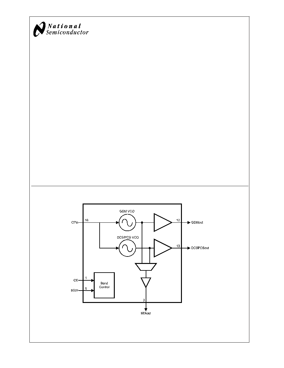
The LMX2604 is a fully integrated VCO (Voltage-Controlled
Oscillator) IC designed for GSM900/DCS1800/PCS1900
triple-band application. The IC is ideal for use in the trans-
mitter modulation loop by providing extremely small form
factor and low phase noise. The IC has two VCOs, one for
GSM and a second for DCS/PCS. The IC has two separate
buffer amplifiers to drive an external high power amplifier,
one for GSM900 band and the other one for DCS1800/
PCS1900 bands. The IC also has a differential buffer ampli-
fier to drive a mixer for the offset PLL.
The resonant circuits of the VCOs are fully integrated in the
chip to ease the application of the IC. The high quality factor
of the embedded tank circuit achieves very low phase noise
characteristics at the VCO output. The only required external
components are a couple of supply bypass capacitors and
matching components.
A control pin for controlling the oscillation frequency is
shared by the two VCOs.
The LMX2604 IC is provided in a 20-pin 4x4 LLP (Leadless
Leadframe package).
Features
n
On-chip Triple-band RF VCOs
GSM: 880 MHz to 915 MHz
DCS: 1710 MHz to 1785 MHz
PCS: 1850 MHz to 1910 MHz
n
On-chip tank circuit
n
Low phase noise
-- -167 dBc/Hz
@
20 MHz offset in GSM band
-- -163 dBc/Hz
@
20 MHz offset in DCS band
-- -162 dBc/Hz
@
20 MHz offset in PCS band
n
High output power
-- +6 dBm in GSM mode
-- +6 dBm in DCS and PCS mode
n
Low current consumption
-- 18 mA in GSM mode
-- 15 mA in DCS and PCS mode
n
+2.6 V to +3.0 V supply voltage
n
0.25 µm RF CMOS process
n
Small 20-pin 4x4 LLP package
Applications
n
Transmit VCO for GSM, DCS, and PCS
n
Closed loop modulation systems
Functional Block Diagram
20066101
FastLock
TM
is a trademark of National Semiconductor Corporation.
TRI-STATE
Æ
is a registered trademark of National Semiconductor Corporation.
January 2004
LMX2604
T
riple-band
VCO
for
GSM900/DCS1800/PCS1900
© 2004 National Semiconductor Corporation
DS200661
www.national.com
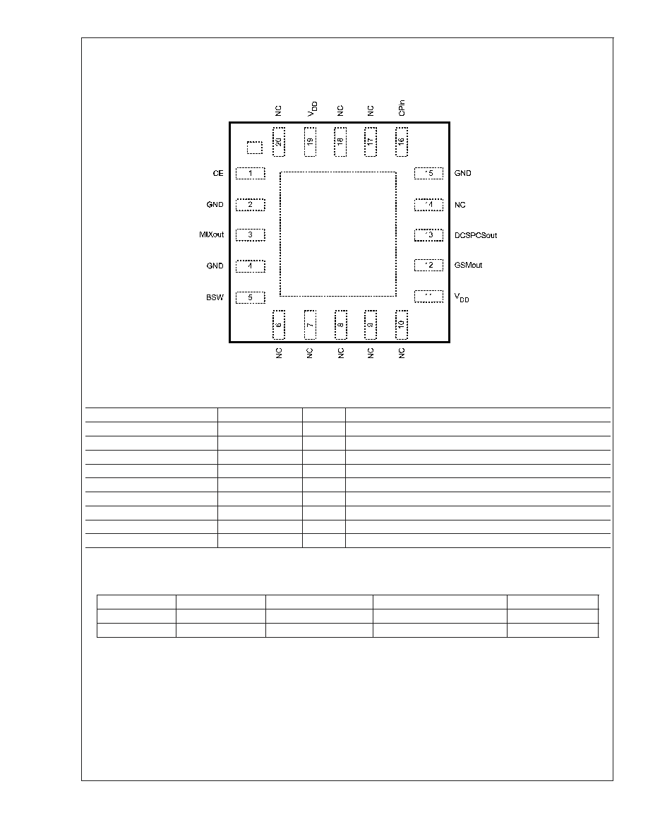
Connection Diagram
20-Pin 4x4 LLP (TM) Package
20066102
Pin Descriptions
Pin Number
Name
I/O
Description
1
CE
I
Chip enable input pin. High=enable, Low=disable
2,4,15
GND (Note 1)
--
Ground pins
3
MIXout
O
Mixer output pin (RF output)
5
BSW
I
Band switch input pin. High=DCS/PCS, Low=GSM
11,19
VDD
--
Supply voltage pins
12
GSMout
O
RF output pin for VCO in GSM band
13
DCSPCSout
O
RF output pin for VCO in DCS and PCS band
16
CPin
I
Charge pump input pin
6,7,8,9,10,14,17,18,20
NC
--
No Connection, These pins must be left open
Note 1: The exposed die attach pad is grounded.
Ordering Information
Package
Part Number
Package Marking
Media Transport
NSC Drawing
20-Pin LLP
LMX2604LQ
LMX2604LQ
1000 Unit Tape and Reel
LQA20A
20-Pin LLP
LMX2604LQX
LMX2604LQ
4500 Unit Tape and Reel
LQA20A
LMX2604
www.national.com
2
Absolute Maximum Ratings
(Notes 3, 4, 5)
Parameter
Symbol
Ratings
Unit
Supply Voltage
V
DD
-0.3 to 3.6
V
Input Voltage
V
IN
-0.3 to V
DD
+0.3
V
Input Current (Note 2)
I
IN
10
mA
Storage Temperature Range
T
STG
-65 to 150
∞C
Note 2: Maximum input current is for a logic pin, not the power pins.
Recommended Operating Conditions
Parameter
Symbol
Condition
Min
Typical
Max
Unit
Ambient Temperature
T
A
V
DD
=3V
-30
25
85
∞C
Supply Voltage (to GND)
V
DD
2.6
2.8
3.0
V
Note 3: "Absolute Maximum Ratings" indicate limits beyond which damage to the device may occur. Operating Ratings indicate conditions for which the device is
intended to be functional, but do not guarantee specific performance limits. For guaranteed specifications and test conditions, see the Electrical Characteristics. The
guaranteed specifications apply only for the test conditions listed.
Note 4: This Device is a high performance RF integrated circuit with an ESD rating
<
2 kV and is ESD sensitive. Handling and assembly of this device should only
be done at ESD-free workstations.
Note 5: Stresses in excess of the absolute maximum ratings can cause permanent or latent damage to the device. These are absolute stress ratings only.
Functional operation of the device is only implied at these or any other conditions in excess of those given in the operation sections of the data sheet. Exposure to
absolute maximum ratings for extended periods can adversely affect device reliability
Electrical Characteristics
AC Characteristics (V
DD
=2.8V, T
A
=25∞C; unless otherwise noted)
Symbol
Parameter
Remarks
Min
Typ
Max
Units
f
Frequency Range
GSM Band
880
915
MHz
DCS Band
1710
1785
MHz
PCS Band
1850
1910
K
VCO
Tuning Sensitivity
(Note 6)
GSM Band
10
15
20
MHz/V
DCS Band
15
20
25
PCS Band
20
25
30
Pout
Output Power
GSM Band
4
6
8
dBm
DCS & PCS Band
4
6
8
PMIXout
Output power of
MIXout pin
GSM Band
-5.5
-3.5
-1.5
dBm
DCS & PCS Band
-4.5
-2.5
-0.5
L(f)
Phase Noise
(GSM Band)
at 100 kHz offset
-120
dBc/Hz
at 400 kHz offset
-136
-128
at 3 MHz offset (Note 7)
-152
at 20 MHz offset (Note 7)
-167
L(f)
Phase Noise
(DCS Band)
at 100 kHz offset
-112
dBc/Hz
at 400 kHz offset
-130
-124
at 3 MHz offset (Note 7)
-146
at 20 MHz offset (Note 7)
-163
L(f)
Phase Noise
(PCS Band)
at 100 kHz offset
-110
dBc/Hz
at 400 kHz offset
-129
-124
at 3 MHz offset (Note 7)
-145
at 20 MHz offset (Note 7)
-162
Second Harmonic
Suppression
All Bands at RF output port.
-20
-15
dBc
Note 6: Tuning Sensitivty is measured after coarse lock. Minimum and maximum limits are supported by characterization.
Note 7: Supported by characterization
LMX2604
www.national.com
3
Electrical Characteristics
(Continued)
DC Characteristics (V
DD
=2.8V, T
A
=25∞C; unless otherwise noted)
Symbol
Parameter
Condition
Min
Typ
Max
Units
V
IH
Logical Input High
Voltage
0.8V
DD
V
DD
+0.3
V
V
IL
Logical Input Low
Voltage
-0.3
0.2V
DD
V
I
IH
Logical Input High
Current
-2.5
2.5
µA
I
IL
Logical Input Low
Current
-2.5
2.5
µA
Input Capacitance
5
pF
I
DD,GSM
Supply Current
(Note 8)
18
21
mA
I
DD,DCS/PCS
Supply Current
(Note 8)
15
18
mA
I
std
Standby Current
2.5
µA
Note 8: The current consumption in VCO and driver amplifier is all included
Note 9: For CE, BSW, and CPin pins
LMX2604
www.national.com
4
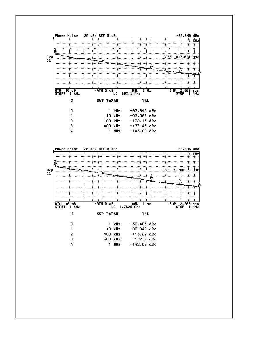
Typical Performance Characteristics : Phase Noise
Typical phase noise characteristics in GSM band
20066161
Typical phase noise characteristics in DCS band
20066162
LMX2604
www.national.com
5