
TL DD 8801
HPC16083HPC26083HPC36083HPC46083HPC16003HPC26003
HPC36003HPC46003
High-Performance
microControllers
PRELIMINARY
April 1994
HPC16083 HPC26083 HPC36083 HPC46083
HPC16003 HPC26003 HPC36003 HPC46003
High-Performance microControllers
General Description
The HPC16083 and HPC16003 are members of the HPC
TM
family of High Performance microControllers Each member
of the family has the same core CPU with a unique memory
and I O configuration to suit specific applications The
HPC16083 has 8k bytes of on-chip ROM The HPC16003
has no on-chip ROM and is intended for use with external
direct memory Each part is fabricated in National's ad-
vanced microCMOS technology This process combined
with an advanced architecture provides fast flexible I O
control efficient data manipulation and high speed compu-
tation
The HPC devices are complete microcomputers on a single
chip All system timing internal logic ROM RAM and I O
are provided on the chip to produce a cost effective solution
for high performance applications On-chip functions such
as UART up to eight 16-bit timers with 4 input capture regis-
ters vectored interrupts WATCHDOG
TM
logic and MICRO-
WIRE PLUS
TM
provide a high level of system integration
The ability to address up to 64k bytes of external memory
enables the HPC to be used in powerful applications typical-
ly performed by microprocessors and expensive peripheral
chips The term ``HPC16083'' is used throughout this data-
sheet to refer to the HPC16083 and HPC16003 devices un-
less otherwise specified
The microCMOS process results in very low current drain
and enables the user to select the optimum speed power
product for his system The IDLE and HALT modes provide
further current savings The HPC is available in 68-pin
PLCC LDCC PGA and 80-Pin PQFP packages
Features
Y
HPC family
core features
16-bit architecture both byte and word
16-bit data bus ALU and registers
64k bytes of external direct memory addressing
FAST
200 ns for fastest instruction when using
20 0 MHz clock 134 ns at 30 MHz
High code efficiency
most instructions are single
byte
16 x 16 multiply and 32 x 16 divide
Eight vectored interrupt sources
Four 16-bit timer counters with 4 synchronous out-
puts and WATCHDOG logic
MICROWIRE PLUS serial I O interface
CMOS
very low power with two power save modes
IDLE and HALT
Y
UART
full duplex programmable baud rate
Y
Four additional 16-bit timer counters with pulse width
modulated outputs
Y
Four input capture registers
Y
52 general purpose I O lines (memory mapped)
Y
8k bytes of ROM 256 bytes of RAM on chip
Y
ROMless version available (HPC16003)
Y
Commercial (0 C to
a
70 C)
industrial (
b
40 C to
a
85 C) automotive (
b
40 C to
a
105 C) and military
(
b
55 C to
a
125 C) temperature ranges
For applications requiring more RAM and ROM see
HPC16064 data sheet
Block Diagram
(HPC16083 with 8k ROM shown)
TL DD 8801 � 1
Series 32000
TapePak
and TRI-STATE
are registered trademarks of National Semiconductor Corporation
MOLE
TM
HPC
TM
COPS
TM
MICROWIRE PLUS
TM
and WATCHDOG
TM
are trademarks of National Semiconductor Corporation
UNIX
is a registered trademarks of AT T Bell Laboratories
VAX
TM
is a trademark of Digital Equipment Corporation
IBM
and PC AT
are registered trademarks of International Business Machines Corporation
SUN
is a registered trademark of Sun Microsystems
SunOS
TM
is a trademark of Sun Microsystems
C1995 National Semiconductor Corporation
RRD-B30M105 Printed in U S A
Absolute Maximum Ratings
If Military Aerospace specified devices are required
please contact the National Semiconductor Sales
Office Distributors for availability and specifications
Total Allowable Source or Sink Current
100 mA
Storage Temperature Range
b
65 C to
a
150 C
Lead Temperature (Soldering 10 sec)
300 C
V
CC
with Respect to GND
b
0 5V to 7 0V
All Other Pins
(V
CC
a
0 5)V to (GND
b
0 5)V
Note
Absolute maximum ratings indicate limits beyond
which damage to the device may occur DC and AC electri-
cal specifications are not ensured when operating the de-
vice at absolute maximum ratings
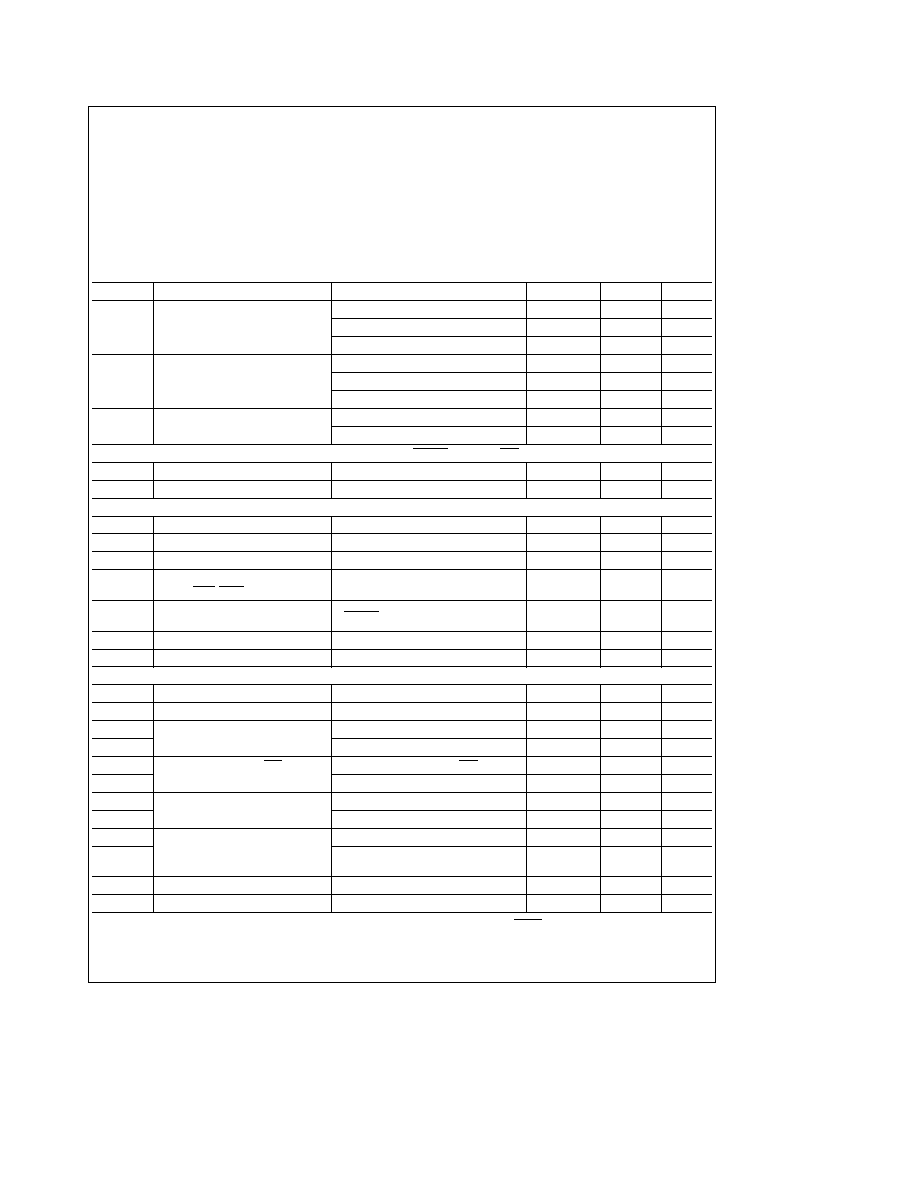
DC Electrical Characteristics
V
CC
e
5 0V
g
10% unless otherwise specified T
A
e
0 C to
a
70 C for
HPC46083 HPC46003
b
40 C to
a
85 C for HPC36083 HPC36003
b
40 C to
a
105 C for
HPC26083 HPC26003
b
55 C to
a
125 C for HPC16083 HPC16003
Symbol
Parameter
Test Conditions
Min
Max
Units
I
CC1
Supply Current
V
CC
e
5 5V f
in
e
30 MHz (Note 1)
65
mA
V
CC
e
5 5V f
in
e
20 MHz (Note 1)
47
mA
V
CC
e
5 5V f
in
e
2 0 MHz (Note 1)
10
mA
I
CC2
IDLE Mode Current
V
CC
e
5 5V f
in
e
30 MHz (Note 1)
5 0
mA
V
CC
e
5 5V f
in
e
20 MHz (Note 1)
3 0
mA
V
CC
e
5 5V f
in
e
2 0 MHz (Note 1)
1
mA
I
CC3
HALT Mode Current
V
CC
e
5 5V f
in
e
0 kHz (Note 1)
200
m
A
V
CC
e
2 5V f
in
e
0 kHz (Note 1)
50
m
A
INPUT VOLTAGE LEVELS FOR SCHMITT TRIGGERED INPUTS RESET NMI AND WO AND ALSO CKI
V
IH1
Logic High
0 9 V
CC
V
V
IL1
Logic Low
0 1 V
CC
V
INPUT VOLTAGE LEVELS FOR ALL OTHER INPUTS
V
IH2
Logic High
0 7 V
CC
V
V
IL2
Logic Low
0 2 V
CC
V
I
LI1
Input Leakage Current
V
IN
e
0 and V
IN
e
V
CC
g
2
m
A
I
LI2
Input Leakage Current
V
IN
e
0
b
3
b
50
m
A
RDY HLD EXUI
I
LI3
Input Leakage Current
RESET
e
0 V
IN
e
V
CC
0 5
7
mA
B12
C
I
Input Capacitance
(Note 2)
10
pF
C
IO
I O Capacitance
(Note 2)
20
pF
OUTPUT VOLTAGE LEVELS
V
OH1
Logic High (CMOS)
I
OH
e b
10 mA (Note 2)
V
CC
b
0 1
V
V
OL1
Logic Low (CMOS)
I
OH
e
10 mA (Note 2)
0 1
V
V
OH2
Port A B Drive CK2
I
OH
e b
7 mA
2 4
V
V
OL2
(A
0
� A
15
B
10
B
11
B
12
B
15
)
I
OL
e
3 mA
0 4
V
V
OH3
Other Port Pin Drive WO (open
I
OH
e b
1 6 mA (except WO)
2 4
V
V
OL3
drain) (B
0
� B
9
B
13
B
14
P
0
� P
3
)
I
OL
e
0 5 mA
0 4
V
V
OH4
ST1 and ST2 Drive
I
OH
e b
6 mA
2 4
V
V
OL4
I
OL
e
1 6 mA
0 4
V
V
OH5
Port A B Drive (A
0
� A
15
I
OH
e b
1 mA
2 4
V
B
10
B
11
B
12
B
15
) when used
V
OL5
as External Address Data Bus
I
OL
e
3 mA
0 4
V
V
RAM
RAM Keep-Alive Voltage
(Note 3)
2 5
V
CC
V
I
OZ
TRI-STATE Leakage Current
V
IN
e
0 and V
IN
e
V
CC
g
5
m
A
Note 1
I
CC1
I
CC2
I
CC3
measured with no external drive (I
OH
and I
OL
e
0 I
IH
and I
IL
e
0) I
CC1
is measured with RESET
e
V
SS
I
CC3
is measured with NMI
e
V
CC
CKI driven to V
IH1
and V
IL1
with rise and fall times less than 10 ns
Note 2
This is guaranteed by design and not tested
Note 3
Test duration is 100 ms
2
20 MHz
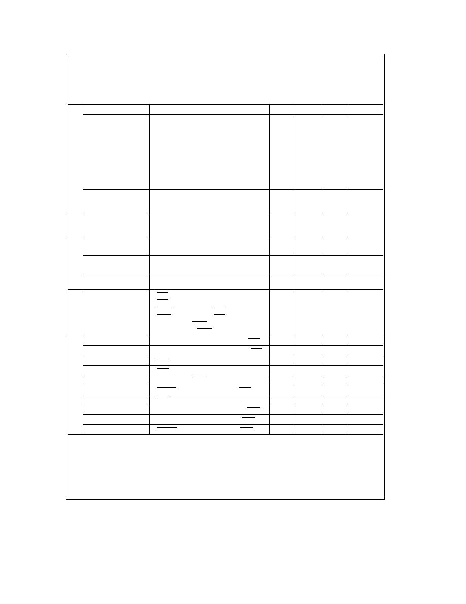
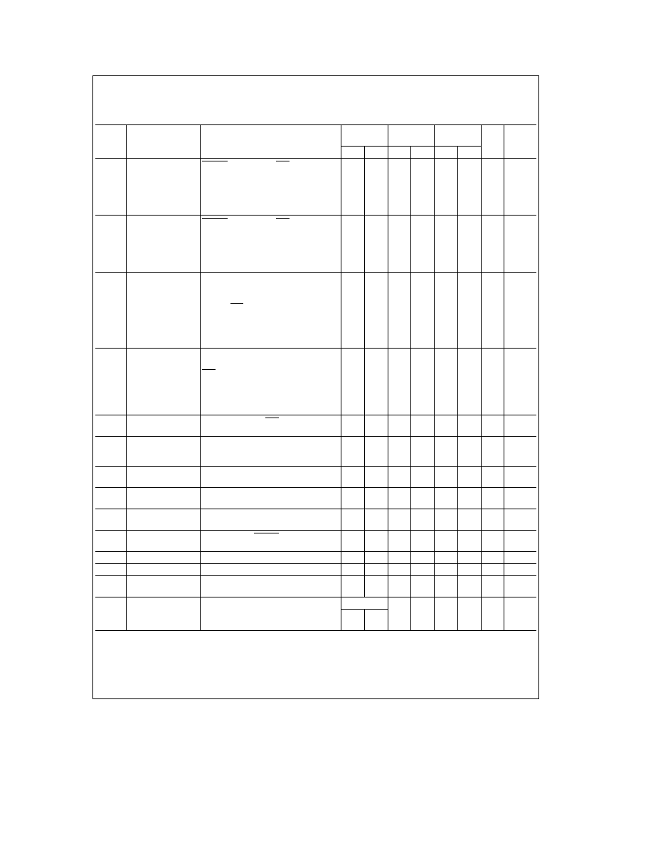
AC Electrical Characteristics
(See Notes 1 and 4 and
Figure 1 thru Figure 5 ) V
CC
e
5 0V
g
10% unless otherwise specified T
A
e
0 C to
a
70 C for
HPC46083 HPC46003
b
40 C to
a
85 C for HPC36083 HPC36003
b
40 C to
a
105 C for HPC26083 HPC26003
b
55 C to
a
125 C for HPC16083 HPC16003
Symbol and Formula
Parameter
Min
Max
Units
Note
f
C
CKI Operating Frequency
2
20
MHz
t
C1
e
1 f
C
CKI Clock Period
50
500
ns
t
CKIH
CKI High Time
22 5
ns
t
CKIL
CKI Low Time
22 5
ns
t
C
e
2 f
C
CPU Timing Cycle
100
ns
t
WAIT
e
t
C
CPU Wait State Period
100
ns
t
DC1C2R
Delay of CK2 Rising Edge after
0
55
ns
(Note 2)
CKI Falling Edge
t
DC1C2F
Delay of CK2 Falling Edge after
0
55
ns
(Note 2)
CKI Falling Edge
f
U
e
f
C
8
External UART Clock Input Frequency
2 5
MHz
f
MW
External MICROWIRE PLUS
1 25
MHz
Clock Input Frequency
f
XIN
e
f
C
22
External Timer Input Frequency
0 91
MHz
t
XIN
e
t
C
Pulse Width for Timer Inputs
100
ns
t
UWS
MICROWIRE Setup Time
Master
100
ns
Slave
20
t
UWH
MICROWIRE Hold Time
Master
20
ns
Slave
50
t
UWV
MICROWIRE Output Valid Time
Master
50
ns
Slave
150
t
SALE
e
t
C
a
40
HLD Falling Edge before ALE Rising Edge
115
ns
t
HWP
e
t
C
a
10
HLD Pulse Width
110
ns
t
HAE
e
t
C
a
100
HLDA Falling Edge after HLD Falling Edge
200
ns
(Note 3)
t
HAD
e
t
C
a
85
HLDA Rising Edge after HLD Rising Edge
160
ns
t
BF
e
t
C
a
66
Bus Float after HLDA Falling Edge
116
ns
(Note 5)
t
BE
e
t
C
a
66
Bus Enable after HLDA Rising Edge
116
ns
(Note 5)
t
UAS
Address Setup Time to Falling Edge of URD
10
ns
t
UAH
Address Hold Time from Rising Edge of URD
10
ns
t
RPW
URD Pulse Width
100
ns
t
OE
URD Falling Edge to Output Data Valid
0
60
ns
t
OD
Rising Edge of URD to Output Data Invalid
5
35
ns
(Note 6)
t
DRDY
RDRDY Delay from Rising Edge of URD
70
ns
t
WDW
UWR Pulse Width
40
ns
t
UDS
Input Data Valid before Rising Edge of UWR
10
ns
t
UDH
Input Data Hold after Rising Edge of UWR
20
ns
t
A
WRRDY Delay from Rising Edge of UWR
70
ns
Clocks
Timers
MICROWIRE
PLUS
External
Hold
UPI
Timing
This maximum frequency is attainable provided that this external baud clock has a duty cycle such that the high period includes two (2) falling edges of the CK2
clock
3
20 MHz
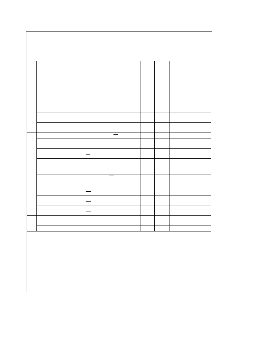
AC Electrical Characteristics
(See Notes 1 and 4 and
Figure 1 thru Figure 5 ) V
CC
e
5 0V
g
10% unless otherwise specified T
A
e
0 C to
a
70 C for
HPC46083 HPC46003
b
40 C to
a
85 C for HPC36083 HPC36003
b
40 C to
a
105 C for HPC26083 HPC26003
b
55 C to
a
125 C for HPC16083 HPC16003 (Continued)
Symbol and Formula
Parameter
Min
Max
Units
Note
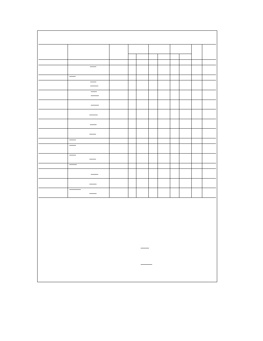
t
DC1ALER
Delay from CKI Rising
0
35
ns
(Notes 1 2)
Edge to ALE Rising Edge
t
DC1ALEF
Delay from CKI Rising
0
35
ns
(Notes 1 2)
Edge to ALE Falling Edge
t
DC2ALER e
tC
a
20
Delay from CK2 Rising
45
ns
(Note 2)
Edge to ALE Rising Edge
t
DC2ALEF e
tC
a
20
Delay from CK2 Rising
45
ns
(Note 2)
Edge to ALE Rising Edge
t
LL
e
t
C
b
9
ALE Pulse Width
41
ns
t
ST
e
t
C
b
7
Setup of Address Valid
18
ns
before ALE Falling Edge
t
VP
e
t
C
b
5
Hold of Address Valid
20
ns
after ALE Falling Edge
t
ARR
e
t
C
b
5
ALE Falling Edge to RD Falling Edge
20
ns
t
ACC
e
t
C
a
WS
b
55
Data Input Valid after
145
ns
(Note 6)
Address Output Valid
t
RD
e
t
C
a
WS
b
65
Data Input Valid after
95
ns
RD Falling Edge
t
RW
e
t
C
a
WS
b
10
RD Pulse Width
140
ns
t
DR
e
t
C
b
15
Hold of Data Input Valid
0
60
ns
after RD Rising Edge
t
RDA
e
t
C
b
15
Bus Enable after RD Rising Edge
85
ns
t
ARW
e
t
C
b
5
ALE Falling Edge to
45
ns
WR Falling Edge
t
WW
e
t
C
a
WS
b
15
WR Pulse Width
160
ns
t
V
e
t
C
a
WS
b
5
Data Output Valid before
145
ns
WR Rising Edge
t
HW
e
t
C
b
5
Hold of Data Valid after
20
ns
WR Rising Edge
t
DAR
e
t
C
a
WS
b
50
Falling Edge of ALE
75
ns
to Falling Edge of RDY
t
RWP
e
t
C
RDY Pulse Width
100
ns
Address
Cycles
Read
Cycles
Write
Cycles
Ready
Input
Note
C
L
e
40 pF
Note 1
These AC characteristics are guaranteed with external clock drive on CKI having 50% duty cycle and with less than 15 pF load on CKO with rise and fall
times (t
CKIR
and T
CKIL
) on CKI input less than 2 5 ns
Note 2
Do not design with these parameters unless CKI is driven with an active signal When using a passive crystal circuit its stability is not guaranteed if either
CKI or CKO is connected to any external logic other than the passive components of the crystal circuit
Note 3
t
HAE
is spec'd for case with HLD falling edge occurring at the latest time it can be accepted during the present CPU cycle being executed If HLD falling
edge occurs later t
HAE
as long as (3t
C
a
4WS
a
72 t
C
a
100) may occur depending on the following CPU instruction cycles its wait state and ready input
Note 4
WS (t
WAIT
) x (number of preprogrammed wait states) Minimum and maximum values are calculated at maximum operating frequency t
C
e
20 MHz with
one wait programmed
Note 5
Due to emulation restrictions
actual limits will be better
Note 6
This is guaranteed by design and not tested
4

30 MHz
AC Electrical Characteristics
(Continued)
(See Notes 1 and 4 and
Figure 1 thru Figure 5 ) V
CC
e
5 0V
g
10% unless otherwise specified T
A
e
0 C to
a
70 C for
HPC46083 HPC46003
b
40 C to
a
85 C for HPC36083 HPC36003
b
40 C to
a
105 C for HPC26083 HPC26003
b
55 C to
a
125 C for HPC16083 HPC16003
Symbol and Formula
Parameter
Min
Max
Units
Note
f
C
CKI Operating Frequency
2
30
MHz
t
C1
e
1 f
C
CKI Clock Period
33
500
ns
t
CKIH
CKI High Time
15
ns
t
CKIL
CKI Low Time
16 6
ns
t
C
e
2 f
C
CPU Timing Cycle
66
ns
t
WAIT
e
t
C
CPU Wait Sate Period
66
ns
t
DC1C2R
Delay of CK2 Rising Edge after
0
55
ns
(Note 2)
CKI Falling Edge
t
DC1C2F
Delay of CK2 Falling Edge after
0
55
ns
(Note 2)
CKI Falling Edge
f
U
e
f
C
8
External UART Clock Input Frequency
3 75
MHz
f
MW
External MICROWIRE PLUS
1 875
MHz
Clock Input Frequency
f
XIN
e
f
C
22
External Timer Input Frequency
1 364
MHz
t
XIN
e
t
C
Pulse Width for Timer Inputs
66
ns
t
UWS
MICROWIRE Setup Time
Master
100
ns
Slave
20
t
UWH
MICROWIRE Hold Time
Master
20
ns
Slave
50
t
UWV
MICROWIRE Output Valid Time
Master
50
ns
Slave
150
t
SALE
e
t
C
a
40
HLD Falling Edge before ALE Rising Edge
90
ns
t
HWP
e
t
C
a
10
HLD Pulse Width
76
ns
t
HAE
e
t
C
a
85
HLDA Falling Edge after HLD Falling Edge
151
ns
(Note 3)
t
HAD
e
t
C
a
85
HLDA Rising Edge after HLD Rising Edge
135
ns
t
BF
e
t
C
a
66
Bus Float after HLDA Falling Edge
99
ns
(Note 5)
t
BE
e
t
C
a
66
Bus Enable after HLDA Rising Edge
99
ns
(Note 5)
t
UAS
Address Setup Time to Falling Edge of URD
10
ns
t
UAH
Address Hold Time from Rising Edge of URD
10
ns
t
RPW
URD Pulse Width
100
ns
t
OE
URD Falling Edge to Output Data Valid
0
60
ns
t
OD
Rising Edge of URD to
5
35
ns
(Note 6)
Output Data Invalid
t
DRDY
RDRDY Delay from Rising Edge of URD
70
ns
t
WDW
UWR Pulse Width
40
ns
t
UDS
Input Data Valid before Rising Edge of UWR
10
ns
t
UDH
Input Data Hold after Rising Edge of UWR
15
ns
t
A
WRRDY Delay from Rising Edge of UWR
70
ns
Clocks
Timers
MICROWIRE
PLUS
External
Hold
UPI
Timing
This maximum frequency is attainable provided that this external baud clock has a duty cycle such that the high period includes two (2) falling edges of the CK2
clock
5
30 MHz
AC Electrical Characteristics
(See Notes 1 and 4 and
Figure 1 thru Figure 5 ) V
CC
e
5 0V
g
10% unless otherwise specified T
A
e
0 C to
a
70 C for
HPC46083 HPC46003
b
40 C to
a
85 C for HPC36083 HPC36003
b
40 C to
a
105 C for HPC26083 HPC26003
b
55 C to
a
125 C for HPC16083 HPC16003 (Continued)
Symbol and Formula
Parameter
Min
Max
Units
Notes
t
DC1ALER
Delay from CKI Rising Edge to ALE Rising Edge
0
35
ns
(Notes 1 2)
t
DC1ALEF
Delay from CKI Rising Edge to ALE Falling Edge
0
35
ns
(Notes 1 2)
t
DC2ALER
e
t
C
a
20
Delay from CK2 Rising Edge to ALE Rising Edge
37
ns
(Note 2)
t
DC2ALEF
e
t
C
a
20
Delay from CK2 Falling Edge to ALE Falling Edge
37
ns
(Note 2)
t
LL
e
t
C
b
9
ALE Pulse Width
24
ns
t
ST
e
t
C
b
7
Setup of Address Valid before ALE Falling Edge
9
ns
t
VP
e
t
C
b
5
Hold of Address Valid after ALE Falling Edge
11
ns
t
ARR
e
t
C
b
5
ALE Falling Edge to RD Falling Edge
12
ns
t
ACC
e
t
C
a
WS
b
32
Data Input Valid after Address Output Valid
100
ns
(Note 6)
t
RD
e
t
C
a
WS
b
39
Data Input Valid after RD Falling Edge
60
ns
t
RW
e
t
C
a
WS
b
14
RD Pulse Width
85
ns
t
DR
e
t
C
b
15
Hold of Data Input Valid after RD Rising Edge
0
35
ns
t
RDA
e
t
C
b
15
Bus Enable after RD Rising Edge
51
ns
t
ARW
e
t
C
b
5
ALE Falling Edge to WR Falling Edge
28
ns
t
WW
e
t
C
a
WS
b
15
WR Pulse Width
101
ns
t
V
e
t
C
a
WS
b
5
Data Output Valid before WR Rising Edge
94
ns
t
HW
e
t
C
b
10
Hold of Data Valid after WR Rising Edge
7
ns
t
DAR
e
t
C
a
WS
b
50
Falling Edge of ALE to Falling Edge of RDY
33
ns
t
RWP
e
t
C
RDY Pulse Width
66
ns
Address
Cycles
Read
Cycles
Write
Cycles
Ready
Input
Note
C
L
e
40 pF
Note 1
These AC characteristics are guaranteed with external clock drive on CKI having 50% duty cycle and with less than 15 pF load on CKO wih rise and fall
times (t
CKIR
and t
CKIL
) on CKI input less than 2 5 ns
Note 2
Do not design with these parameters unless CKI is driven with an active signal When using a passive crystal circuit its stability is not guaranteed if either
CKI or CKO is connected to any external logic other than the passive components of the crystal circuit
Note 3
t
HAE
is spec'd for case with HLD falling edge occurring at the latest time it can be accepted during the present CPU cycle being executed If HLD falling
edge occurs later t
HAE
as long as (3t
C
a
4WS
a
72 t
C
a
100) may occur depending on the following CPU instruction cycles its wait states and ready input
Note 4
WS t
WAIT
c
(number of pre-programmed wait states) Minimum and maximum values are calculated from maximum operating frequency t
C
e
30 MHz
with one wait state programmed
Note 5
Due to emulation restrictions
actual limits will be better
Note 6
This is guaranteed by design and not tested
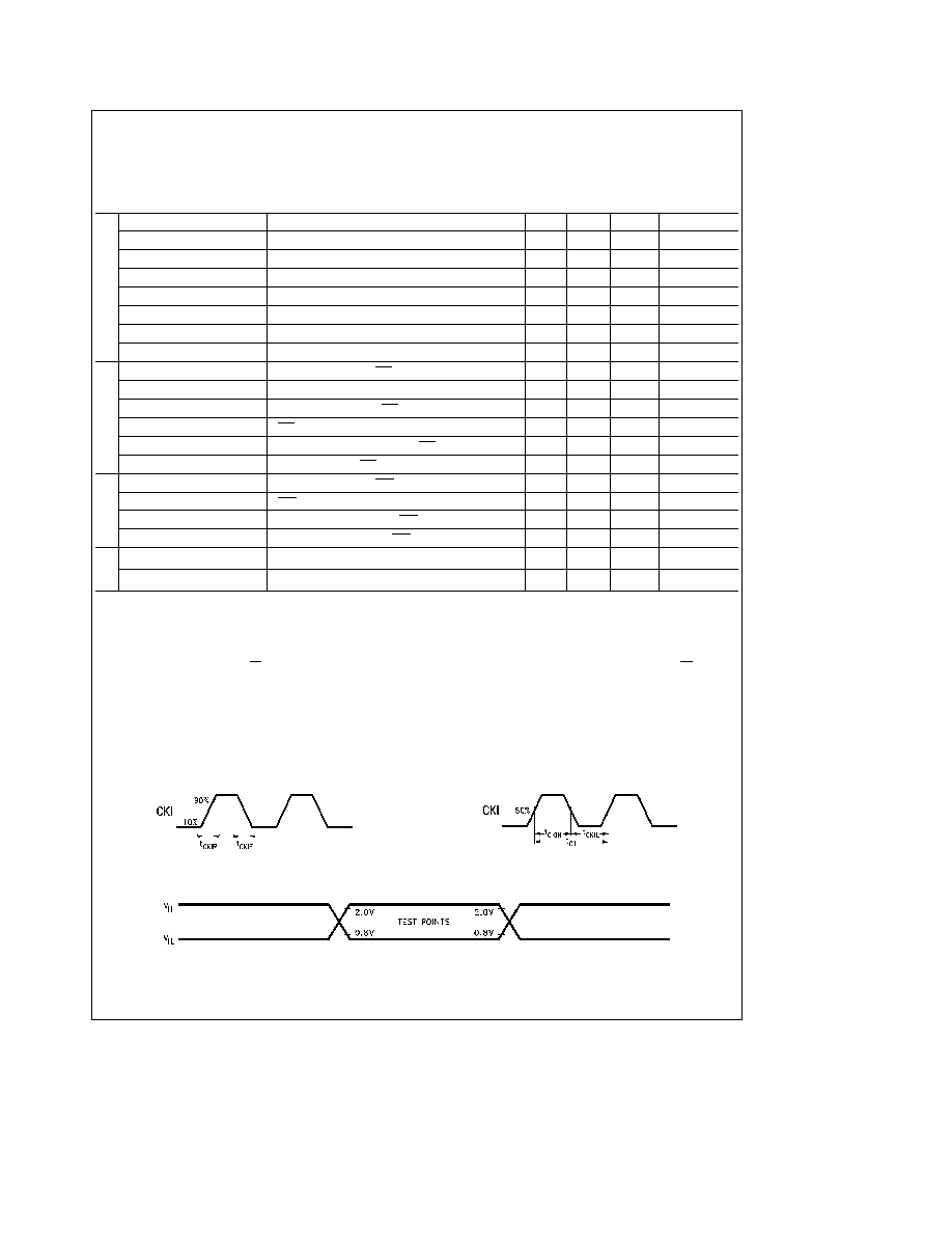
CKI Input Signal Characteristics
Rise Fall Time
TL DD 8801 � 35
Duty Cycle
TL DD 8801 � 36
FIGURE 1 CKI Input Signal
TL DD 8801 � 38
FIGURE 2 Input and Output for AC Tests
Note
AC testing inputs are driven at V
IH
for a logic ``1'' and V
IL
for a logic ``0'' Output timing measurements are made at 2 0V for a logic ``1'' and 0 8V for a logic
``0''
6
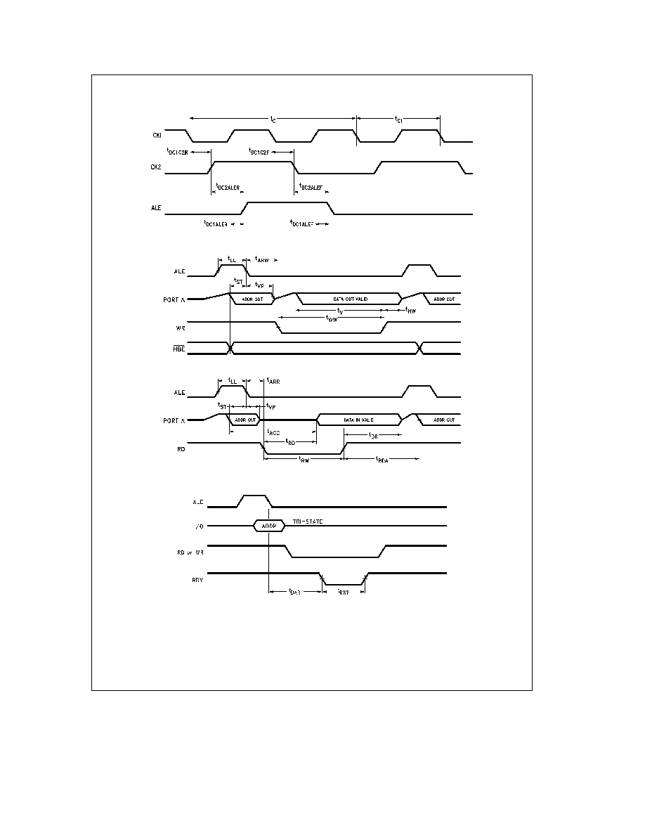
Timing Waveforms
TL DD 8801 � 33
FIGURE 3 CKI CK2 ALE Timing Diagram
TL DD 8801 � 3
FIGURE 4 Write Cycle
TL DD 8801 � 4
FIGURE 5 Read Cycle
TL DD 8801 � 5
FIGURE 6 Ready Mode Timing
7
Timing Waveforms
(Continued)
TL DD 8801 � 6
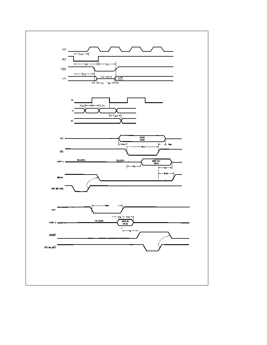
FIGURE 7 Hold Mode Timing
TL DD 8801 � 37
FIGURE 8 MICROWIRE Setup Hold Timing
TL DD 8801 � 9
FIGURE 9 UPI Read Timing
TL DD 8801 � 10
FIGURE 10 UPI Write Timing
8
The following is the Military 883 Electrical Specification for HPC16083 and HPC16003 For latest information on RETS 16083X
contact NSC local sales office
DC Electrical Specifications
Test Conditions V
CC
e
5V
g
10% (Unless Otherwise Specified) (Note 1)
Symbol
Parameter
Conditions
SBGRP 1
SBGRP 2
SBGRP 3
Units
Notes
a
25 C
a
125 C
b
55 C
Min
Max
Min
Max
Min
Max
V
IH1
Logical ``1'' Input
RESET NMI CKI and WO
0 9
0 9
0 9
V
Voltage
B
10
� B
13
B
15
(V
CC
)
(V
CC
)
(V
CC
)
V
IH2
All Inputs except Port A
0 7
0 7
0 7
V
(V
CC
)
(V
CC
)
(V
CC
)
V
IH3
Port A V
CC
e
5 5V
4 65
4 65
4 65
V
(Note 2)
Port A V
CC
e
4 5V
3 95
3 95
3 95
V
(Note 2)
V
IL1
Logical ``0'' Input
RESET NMI CKI and WO
0 1
0 1
0 1
V
Voltage
(V
CC
)
(V
CC
)
(V
CC
)
V
IL2
All Inputs except Port A
0 2
0 2
0 2
V
(V
CC
)
(V
CC
)
(V
CC
)
V
IL3
Port A V
CC
e
5 5V
0 7
0 7
0 7
V
(Note 3)
Port A V
CC
e
4 5V
0 5
0 5
0 5
V
(Note 3)
V
OH2
Logical ``1'' Output
I
OH
e b
7 mA (A
0
� A
15
2 4
2 4
2 4
V
Voltage
B
10
� B
12
B
15
CK2)
V
OH3
I
OH3
e b
1 6 mA (B
0
� B
9
B
13
� B
14
2 4
2 4
2 4
V
P
0
� P
3
) WO (Open Drain)
V
OH4
I
OH
e b
6 mA (ST1 ST2)
2 4
2 4
2 4
V
V
OH5
I
OH
e b
1 mA (A
0
� A
15
B
10
� B
12
B
15
)
When Used as an External
2 4
2 4
2 4
V
Address Data Bus
V
OL2
Logical ``0'' Output
I
OL
e
3 mA (CK2 A
0
� A
15
B
10
-B
12
B
15
)
0 4
0 4
0 4
V
V
OL3
Voltage
I
OL
e
0 5 mA (B
0
� B
9
B
13
-B
14
P
0
� P
3
0 4
0 4
0 4
V
WO (Open Drain)
V
OL4
I
OL
e
1 6 mA (ST1 ST2)
0 4
0 4
0 4
V
V
OL5
I
OL
e
3 mA (A
0
� A
15
B
10
� B
12
B
15
)
When Used as an External
0 4
0 4
0 4
V
Address Data Bus
I
OZ
TRI-STATE Leakage V
SS
s
V
IN
s
V
CC
(WO Port A
g
5
g
5
g
5
m
A
Port B) V
CC
e
5 5V
I
LI1
Input Leakage
V
SS
s
V
IN
s
V
CC
V
CC
e
5 5V
Current
(I
1
� I
6
D
0
� D
7
CKI
g
2
g
2
g
2
m
A
(Note 7)
RESET EXM EI)
I
LI2
Input Pullup Current
V
IN
e
0 (I
0
I
7
RDY HLD
b
50
b
3
b
50
b
3
b
50
b
3
m
A
(Note 7)
EXUI) V
CC
e
5 5V
I
LI3
Port B
12
Pulldown
V
IN
e
V
CC
Port B
12
1
7
1
7
1
7
mA
during Reset
V
CC
e
5 5V
VRAM
RAM Keep Alive
Test Duration is 10 ms
2 5
2 5
2 5
V
Voltage
I
CC1
Supply Current
F
IN
e
20 MHz RESET
e
V
SS
55
55
55
mA
Dynamic
I
OH
e
0 mA I
OL
e
0 mA V
CC
e
5 5V
I
CC2
Idle Mode Current
F
IN
e
20 MHz External Clock
3 5
3 5
3 5
mA
I
CC
Halt Mode Current
NMI
e
V
CC
2
2
2
mA
CI O
Input Output
f
test
e
1 0 MHz
20
pF
(Note 4)
Capacitance
I O Pin to Ground
SBGRP4
CI
Input Capacitance
f
test
e
1 0 MHz
10
pF
(Note 4)
Input Pin to Ground
Note 1
Electrical end point testing (when required) for Groups C
D shall consist only of subgroups 1 2 9 and 10
Note 2
Port A V
IH
test limit includes 700 mV offset caused by output loads being on during Data Drive Time
Note 3
Port A V
IL
test limit includes 400 mV offset caused by output loads being on during Data Drive Time
Note 4
Verified at initial qual only
Note 7
Future revisions of this device will not have pullups on pins I
0
I
7
which will be tested to I
LI1
conditions
9

AC Electrical Specifications
Test Conditions V
CC
e
4 5V and 5 5V (Unless Otherwise Specified) (Note 1)
Symbol
Parameter
Conditions
SBGRP 9
SBGRP 10
SBGRP 11
Units
Notes
a
25 C
a
125 C
b
55 C
Min
Max
Min
Max
Min
Max
f
C
e
CKI Freq
Operating Frequency
2
20
2
20
2
20
MHz
(Note 5)
t
CI
e
1 FC
Clock Period
50
50
50
ns
(Note 5)
t
C
e
2 FC
Timing Cycle
100
100
100
ns
(Note 5)
t
LL
e
t
C
b
9
ALE Pulse Width
41
41
41
ns
(Note 6)
t
ST
e
t
C
b
7
Address Valid to
18
18
18
ns
(Note 6)
ALE Falling Edge
t
WAIT
e
t
C
e
WS
Wait State Period
100
100
100
ns
(Note 5)
FMW
e
0 0625 f
C
External MICROWIRE PLUS
1 25
1 25
1 25
MHz
(Note 6)
CLK Input Frequency
f
U
e
0 125 f
C
External UART
2 5
2 5
2 5
MHz
(Note 5)
Clock Input Frequency
t
DCIC2
CK2 Delay From CK1
55
55
55
ns
(Note 6)
t
ARR
e
t
C
b
5
ALE Falling Edge
20
20
20
ns
(Note 6)
to RD Falling Edge
t
RW
e
RD Pulse Width
140
140
140
ns
(Note 6)
t
C
a
WS
b
10
t
DR
e
3 4 t
C
b
15
Data Hold after
0
60
0
60
0
60
ns
(Note 6)
Rising Edge of RD
t
RD
e
RD Falling Edge to
85
85
85
ns
(Note 6)
t
C
a
WS
b
65
Data in Valid
t
RDA
e
t
C
b
15
RD Rising Edge to
85
85
85
ns
(Note 6)
Address Valid
t
VP
e
t
C
b
5
Address Hold from
20
20
20
ns
(Note 6)
ALE Falling Edge
t
ARW
e
t
C
b
5
ALE Trailing Edge
45
45
45
ns
(Note 6)
to WR Falling Edge
t
WW
e
t
C
a
WS
b
15
WR Pulse Width
160
160
160
ns
(Note 6)
t
HW
e
t
C
b
5
Data Hold after
20
20
20
ns
(Note 6)
Trailing Edge of WR
t
V
e
t
C
a
WS
b
5
Data Valid before
145
145
145
ns
(Note 6)
Rising Edge of WR
t
DAR
e
t
C
a
WS
b
50
Falling Edge of ALE
75
75
75
ns
(Note 6)
to Falling Edge of RDY
10
AC Electrical Specifications
Test Conditions V
CC
e
4 5V and 5 5V (Unless Otherwise Specified) (Note 1)
(Continued)
Symbol
Parameter
Conditions
SBGRP 9
SBGRP 10
SBGRP 11
Units
Notes
a
25 C
a
125 C
b
55 C
Min
Max
Min
Max
Min
Max
t
RWP
e
t
C
RDY Pulse Width
100
100
100
ns
(Note 6)
t
SALE
e
t
C
a
40
Falling Edge of HLD to
115
115
115
ns
(Note 6)
to Rising Edge of ALE
t
HWP
e
t
C
a
10
HLD Pulse Width
110
110
110
ns
(Note 6)
t
HAD
e
t
C
a
85
Rising Edge on HLD to
160
160
160
ns
(Note 6)
Rising Edge on HLDA
t
HAE
e
t
C
a
100
Falling Edge on HLD to
200
200
200
ns
(Note 6)
Falling Edge on HLDA
t
BF
e
t
C
a
66
BUS Float before
116
116
116
ns
(Note 6)
Falling Edge on HLDA
t
BE
e
t
C
a
66
BUS Enable from
116
116
116
ns
(Note 6)
Rising Edge of HLDA
t
UAS
Address Setup Time to
10
10
10
ns
(Note 6)
Falling Edge of URD
t
UAH
Address Hold Time from
10
10
10
ns
(Note 6)
Rising Edge of URD
t
RPW
URD Pulse Width
100
100
100
ns
(Note 6)
t
OE
URD Falling Edge to
60
60
60
ns
(Note 6)
Data Out Valid
t
RDRDY
RDY Delay from
70
70
70
ns
(Note 6)
Rising Edge of URD
t
WDW
UWR Pulse Width
40
40
40
ns
(Note 6)
t
UDS
Data Invalid before
10
10
10
ns
(Note 6)
Trailing Edge of UWR
t
UDH
Data In Hold after
15
15
15
ns
(Note 6)
Rising Edge of UWR
t
A
WRRDY Delay from
70
70
70
ns
(Note 6)
Rising Edge of UWR
Note 1
Electrical end point testing (when required) for groups C
D shall consist only of subgroups 1 2 9 and 10
Note 5
Tested in functional patterns Not directly measured
Note 6
C
L
e
70 pF Input and output levels are per DC characteristics
Pin Descriptions
The HPC16083 is available in 68-pin PLCC LDCC PGA
and 80-pin PQFP packages
I O PORTS
Port A is a 16-bit bidirectional I O port with a data direction
register to enable each separate pin to be individually de-
fined as an input or output When accessing external memo-
ry port A is used as the multiplexed address data bus
Port B is a 16-bit port with 12 bits of bidirectional I O similar
in structure to Port A Pins B10 B11 B12 and B15 are gen-
eral purpose outputs only in this mode Port B may also be
configured via a 16-bit function register BFUN to individually
allow each pin to have an alternate function
B0
TDX
UART Data Output
B1
B2
CKX
UART Clock (Input or Output)
B3
T2IO
Timer2 I O Pin
B4
T3IO
Timer3 I O Pin
B5
SO
MICROWIRE PLUS Output
B6
SK
MICROWIRE PLUS Clock (Input or Output)
B7
HLDA
Hold Acknowledge Output
B8
TS0
Timer Synchronous Output
B9
TS1
Timer Synchronous Output
B10
UA0
Address 0 Input for UPI Mode
B11
WRRDY Write Ready Output for UPI Mode
B12
B13
TS2
Timer Synchronous Output
11

Pin Descriptions
(Continued)
B14
TS3
Timer Synchronous Output
B15
RDRDY
Read Ready Output for UPI Mode
When accessing external memory four bits of port B
are used as follows
B10
ALE
Address Latch Enable Output
B11
WR
Write Output
B12
HBE
High Byte Enable Output Input
(sampled at reset)
B15
RD
Read Output
Port I is an 8-bit input port that can be read as general
purpose inputs and is also used for the following functions
I0
I1
NMI
Nonmaskable Interrupt Input
I2
INT2
Maskable Interrupt Input Capture URD
I3
INT3
Maskable Interrupt Input Capture UWR
I4
INT4
Maskable Interrupt Input Capture
I5
SI
MICROWIRE PLUS Data Input
I6
RDX
UART Data Input
I7
Port D is an 8-bit input port that can be used as general
purpose digital inputs
Port P is a 4-bit output port that can be used as general
purpose data or selected to be controlled by timers 4
through 7 in order to generate frequency duty cycle and
pulse width modulated outputs
POWER SUPPLY PINS
V
CC1
and
V
CC2
Positive Power Supply
GND
Ground for On-Chip Logic
DGND
Ground for Output Buffers
Note
There are two electrically connected V
CC
pins on the chip GND and
DGND are electrically isolated Both V
CC
pins and both ground pins
must be used
CLOCK PINS
CKI
The Chip System Clock Input
CKO
The Chip System Clock Output (inversion of CKI)
Pins CKI and CKO are usually connected across an external
crystal
CK2
Clock Output (CKI divided by 2)
OTHER PINS
WO
This is an active low open drain output that sig-
nals an illegal situation has been detected by the
Watch Dog logic
ST1
Bus Cycle Status Output indicates first opcode
fetch
ST2
Bus Cycle Status Output
indicates machine
states (skip interrupt and first instruction cycle)
RESET
is an active low input that forces the chip to re-
start and sets the ports in a TRI-STATE mode
RDY HLD has two uses selected by a software bit It's ei-
ther a READY input to extend the bus cycle for
slower memories or a HOLD request input to put
the bus in a high impedance state for DMA pur-
poses
NC
(no connection) do not connect anything to this
pin
EXM
External memory enable (active high) disables
internal ROM and maps it to external memory
EI
External
interrupt
with
vector
address
FFF1 FFF0 (Rising falling edge or high low lev-
el sensitive) Alternately can be configured as
4th input capture
EXUI
External interrupt which is internally OR'ed with
the
UART
interrupt
with
vector
address
FFF3 FFF2 (Active Low)
Connection Diagrams
Plastic and Ceramic Leaded Chip Carriers
TL DD 8801 � 11
Top View
See NS Package Number EL68A or V68A
See Part Selection for Ordering Information
12

Connection Diagrams
(Continued)
Plastic Quad Flatpack
TL DD 8801 � 34
Top View
See NS Package Number VJE80A
See Part Selection for Ordering Information
Pin Grid Array Pinout
TL DD 8801 � 12
Top View
(looking down on component side of PC Board)
See NS Package Number U68A
See Part Selection for Ordering Information
13

Ports A
B
The highly flexible A and B ports are similarly structured
The Port A (see
Figure 11 ) consists of a data register and a
direction register Port B (see
Figures 12 13 14 ) has an
alternate function register in addition to the data and direc-
tion registers All the control registers are read write regis-
ters
The associated direction registers allow the port pins to be
individually programmed as inputs or outputs Port pins se-
lected as inputs are placed in a TRI-STATE mode by reset-
ting corresponding bits in the direction register
A write operation to a port pin configured as an input causes
the value to be written into the data register a read opera-
tion returns the value of the pin Writing to port pins config-
ured as outputs causes the pins to have the same value
reading the pins returns the value of the data register
Primary and secondary functions are multiplexed onto Port
B through the alternate function register (BFUN) The sec-
ondary functions are enabled by setting the corresponding
bits in the BFUN register
TL DD 8801 � 13
FIGURE 11 Port A I O Structure
TL DD 8801 � 14
FIGURE 12 Structure of Port B Pins B0 B1 B2 B5 B6 and B7 (Typical Pins)
14

Ports A
B
(Continued)
TL DD 8801 � 15
FIGURE 13 Structure of Port B Pins B3 B4 B8 B9 B13 and B14 (Timer Synchronous Pins)
TL DD 8801 � 16
FIGURE 14 Structure of Port B Pins B10 B11 B12 and B15 (Pins with Bus Control Roles)
15
Operating Modes
To offer the user a variety of I O and expanded memory
options the HPC16083 has four operating modes The
ROMless HPC16003 has one mode of operation The vari-
ous modes of operation are determined by the state of both
the EXM pin and the EA bit in the PSW register The state of
the EXM pin determines whether on-chip ROM will be ac-
cessed or external memory will be accessed within the ad-
dress range of the on-chip ROM The on-chip ROM range of
the HPC16083 is E000 to FFFF (8k bytes) The HPC16003
has no on-chip ROM and is intended for use with external
memory for program storage A logic ``0'' state on the EXM
pin will cause the HPC device to address on-chip ROM
when the Program Counter (PC) contains addresses within
the on-chip ROM address range A logic ``1'' state on the
EXM pin will cause the HPC device to address memory that
is external to the HPC when the PC contains on-chip ROM
addresses The EXM pin should always be pulled high (logic
``1'') on the HPC16003 because no on-chip ROM is avail-
able The function of the EA bit is to determine the legal
addressing range of the HPC device A logic ``0'' state in the
EA bit of the PSW register does two things
addresses are
limited to the on-chip ROM range and on-chip RAM and
Register range and the ``illegal address detection'' feature
of the WATCHDOG logic is engaged A logic ``1'' in the EA
bit enables accesses to be made anywhere within the 64k
byte address range and the ``illegal address detection'' fea-
ture of the WATCHDOG logic is disabled The EA bit should
be set to ``1'' by software when using the HPC16003 to
disable the ``illegal address detection'' feature of WATCH-
DOG
All HPC devices can be used with external memory Exter-
nal memory may be any combination of RAM and ROM
Both 8-bit and 16-bit external data bus modes are available
Upon entering an operating mode in which external memory
is used port A becomes the Address Data bus Four pins of
port B become the control lines ALE RD WR and HBE The
High Byte Enable pin (HBE) is used in 16-bit mode to select
high order memory bytes The RD and WR signals are only
generated if the selected address is off-chip The 8-bit mode
is selected by pulling HBE high at reset If HBE is left float-
ing or connected to a memory device chip select at reset
the 16-bit mode is entered The following sections describe
the operating modes of the HPC16083 and HPC16003
Note
The HPC devices use 16-bit words for stack memory Therefore
when using the 8-bit mode User's Stack must be in internal RAM
HPC16083 Operating Modes
SINGLE CHIP NORMAL MODE
In this mode the HPC16083 functions as a self-contained
microcomputer (see
Figure 15 ) with all memory (RAM and
ROM) on-chip It can address internal memory only consist-
ing of 8k bytes of ROM (E000 to FFFF) and 256 bytes of on-
chip RAM and registers (0000 to 01FF) The ``illegal address
detection'' feature of the WATCHDOG is enabled in the Sin-
gle-Chip Normal mode and a WATCHDOG Output (WO) will
occur if an attempt is made to access addresses that are
outside of the on-chip ROM and RAM range of the device
Ports A and B are used for I O functions and not for ad-
dressing external memory The EXM pin and the EA bit of
the PSW register must both be logic ``0'' to enter the Single-
Chip Normal mode
EXPANDED NORMAL MODE
The Expanded Normal mode of operation enables the
HPC16083 to address external memory in addition to the
on-chip ROM and RAM (see Table I) WATCHDOG illegal
address detection is disabled and memory accesses may
be made anywhere in the 64k byte address range without
triggering an illegal address condition The Expanded Nor-
mal mode is entered with the EXM pin pulled low (logic ``0'')
and setting the EA bit in the PSW register to ``1''
SINGLE-CHIP ROMLESS MODE
In this mode the on-chip mask programmed ROM of the
HPC16083 is not used The address space corresponding
to the on-chip ROM is mapped into external memory so 8k
bytes of external memory may be used with the HPC16083
(see Table I) The WATCHDOG circuitry detects illegal ad-
dresses (addresses not within the on-chip ROM and RAM
range) The Single-Chip ROMless mode is entered when the
EXM pin is pulled high (logic ``1'') and the EA bit is logic ``0''
EXPANDED ROMLESS MODE
This mode of operation is similar to Single-Chip ROMless
mode in that no on-chip ROM is used however a full 64k
bytes of external memory may be used The ``illegal address
detection'' feature of WATCHDOG is disabled The EXM pin
must be pulled high (logic ``1'') and the EA bit in the PSW
register set to ``1'' to enter this mode
TABLE I HPC16083 Operating Modes
Operating
EXM
EA
Memory
Mode
Pin
Bit
Configuration
Single-Chip Normal
0
0
E000 FFFF on-chip
Expanded Normal
0
1
E000 FFFF on-chip
0200 DFFF off-chip
Single-Chip ROMless
1
0
E000 FFFF off-chip
Expanded ROMless
1
1
0200 FFFF off-chip
Note
In all operating modes the on-chip RAM and Registers (0000 01FF)
may be accessed
16

HPC16003 Operating Modes
EXPANDED ROMLESS MODE (HPC16003)
Because the HPC16003 has no on-chip ROM it has only
one mode of operation the Expanded ROMless Mode The
EXM pin must be pulled high (logic ``1'') on power up the
EA bit in the PSW register should be set to a ``1'' The
HPC16003 is a ROMless device and is intended for use with
external memory The external memory may be any combi-
nation of ROM and RAM Up to 64k bytes of external mem-
ory may be accessed It is necessary to vector on reset to
an address between F000 and FFFF therefore the user
should have external memory at these addresses The EA
bit in the PSW register must immediately be set to ``1'' at the
beginning of the user's program to disable illegal address
detection in the WATCHDOG logic
TABLE II HPC16003 Operating Modes
Operating
EXM
EA
Memory
Mode
Pin
Bit
Configuration
Expanded ROMless
1
1
0200 FFFF off-chip
Note
The on-chip RAM and Registers (0000 01FF) of the HPC16003 may
be accessed at all times
TL DD 8801 � 17
FIGURE 15 Single-Chip Mode
TL DD 8801 � 18
FIGURE 16 8-Bit External Memory
17
HPC16003 Operating Modes
(Continued)
TL DD 8801 � 19
FIGURE 17 16-Bit External Memory
Wait States
The internal ROM can be accessed at the maximum operat-
ing frequency with one wait state With 0 wait states internal
ROM accesses are limited to
f
C
max
The HPC16083 provides four software selectable Wait
States that allow access to slower memories The Wait
States are selected by the state of two bits in the PSW
register Additionally the RDY input may be used to extend
the instruction cycle allowing the user to interface with slow
memories and peripherals
Power Save Modes
Two power saving modes are available on the HPC16083
HALT and IDLE In the HALT mode all processor activities
are stopped In the IDLE mode the on-board oscillator and
timer T0 are active but all other processor activities are
stopped In either mode all on-board RAM registers and
I O are unaffected
HALT MODE
The HPC16083 is placed in the HALT mode under software
control by setting bits in the PSW All processor activities
including the clock and timers are stopped In the HALT
mode power requirements for the HPC16083 are minimal
and the applied voltage (V
CC
) may be decreased without
altering the state of the machine There are two ways of
exiting the HALT mode via the RESET or the NMI The
RESET input reinitializes the processor Use of the NMI in-
put will generate a vectored interrupt and resume operation
from that point with no initialization The HALT mode can be
enabled or disabled by means of a control register HALT
enable To prevent accidental use of the HALT mode the
HALT enable register can be modified only once
IDLE MODE
The HPC16083 is placed in the IDLE mode through the
PSW In this mode all processor activity except the on-
board oscillator and Timer T0 is stopped As with the HALT
mode the processor is returned to full operation by the
RESET or NMI inputs but without waiting for oscillator stabi-
lization A timer T0 overflow will also cause the HPC16083
to resume normal operation
HPC16083 Interrupts
Complex interrupt handling is easily accomplished by the
HPC16083's vectored interrupt scheme There are eight
possible interrupt sources as shown in Table III
TABLE III Interrupts
Vector
Interrupt
Arbitration
Address
Source
Ranking
FFFF FFFE
RESET
0
FFFD FFFC
Nonmaskable external on
1
rising edge of I1 pin
FFFB FFFA
External interrupt on I2 pin
2
FFF9 FFF8
External interrupt on I3 pin
3
FFF7 FFF6
External interrupt on I4 pin
4
FFF5 FFF4
Overflow on internal timers
5
FFF3 FFF2
Internal on the UART
transmit receive complete
6
or external on EXUI
FFF1 FFF0
External interrupt on EI pin
7
18

Interrupt Arbitration
The HPC16083 contains arbitration logic to determine which
interrupt will be serviced first if two or more interrupts occur
simultaneously The arbitration ranking is given in Table III
The interrupt on RESET has the highest rank and is serv-
iced first
Interrupt Processing
Interrupts are serviced after the current instruction is com-
pleted except for the RESET which is serviced immediately
RESET and EXUI are level-LOW-sensitive interrupts and EI
is programmable for edge-(RISING or FALLING) or level-
(HIGH or LOW) sensitivity All other interrupts are edge-sen-
sitive NMI is positive-edge sensitive The external interrupts
on I2 I3 and I4 can be software selected to be rising or
falling edge External interrupt (EXUI) is shared with the
UART interrupt This interrupt is level-low sensitive To se-
lect this interrupt disable the ERI and ETI UART interrupt
bits in the ENUI register To select the UART interrupt leave
this pin floating or tie it high
Interrupt Control Registers
The HPC16083 allows the various interrupt sources and
conditions to be programmed This is done through the vari-
ous control registers A brief description of the different con-
trol registers is given below
INTERRUPT ENABLE REGISTER (ENIR)
RESET and the External Interrupt on I1 are non-maskable
interrupts The other interrupts can be individually enabled
or disabled Additionally a Global Interrupt Enable Bit in the
ENIR Register allows the Maskable interrupts to be collec-
tively enabled or disabled Thus in order for a particular
interrupt to request service both the individual enable bit
and the Global Interrupt bit (GIE) have to be set
INTERRUPT PENDING REGISTER (IRPD)
The IRPD register contains a bit allocated for each interrupt
vector The occurrence of specified interrupt trigger condi-
tions causes the appropriate bit to be set There is no indi-
cation of the order in which the interrupts have been re-
ceived The bits are set independently of the fact that the
interrupts may be disabled IRPD is a Read Write register
The bits corresponding to the maskable external interrupts
are normally cleared by the HPC16083 after servicing the
interrupts
For the interrupts from the on-board peripherals the user
has the responsibility of resetting the interrupt pending flags
through software
The NMI bit is read only and I2 I3 and I4 are designed as to
only allow a zero to be written to the pending bit (writing a
one has no affect) A LOAD IMMEDIATE instruction is to be
the only instruction used to clear a bit or bits in the IRPD
register This allows a mask to be used thus ensuring that
the other pending bits are not affected
INTERRUPT CONDITION REGISTER (IRCD)
Three bits of the register select the input polarity of the
external interrupt on I2 I3 and I4
Servicing the Interrupts
The Interrupt once acknowledged pushes the program
counter (PC) onto the stack thus incrementing the stack
pointer (SP) twice The Global Interrupt Enable bit (GIE) is
copied into the CGIE bit of the PSW register it is then reset
thus disabling further interrupts The program counter is
loaded with the contents of the memory at the vector ad-
dress and the processor resumes operation at this point At
the end of the interrupt service routine the user does a
RETI instruction to pop the stack and re-enable interrupts if
the CGIE bit is set or RET to just pop the stack if the CGIE
bit is clear and then returns to the main program The GIE
bit can be set in the interrupt service routine to nest inter-
rupts if desired
Figure 18 shows the Interrupt Enable Logic
RESET
The RESET input initializes the processor and sets ports A
and B in the TRI-STATE condition and port P in the LOW
state RESET is an active-low Schmitt trigger input The
processor vectors to FFFF FFFE and resumes operation at
the address contained at that memory location (which must
correspond to an on board location) The Reset vector ad-
dress must be between E000 and FFFF when using the
HPC16003
19

TLDD8801
�
2
0
FIGURE
18
Block
Diagram
of
Interrupt
Logic
20
Timer Overview
The HPC16083 contains a powerful set of flexible timers
enabling the HPC16083 to perform extensive timer func-
tions not usually associated with microcontrollers
The HPC16083 contains nine 16-bit timers Timer T0 is a
free-running timer counting up at a fixed CKI 16 (Clock In-
put 16) rate It is used for WATCHDOG logic high speed
event capture and to exit from the IDLE mode Conse-
quently it cannot be stopped or written to under software
control Timer T0 permits precise measurements by means
of the capture registers I2CR I3CR and I4CR A control bit
in the register TMMODE configures timer T1 and its associ-
ated register R1 as capture registers I3CR and I2CR The
capture registers I2CR I3CR and I4CR respectively record
the value of timer T0 when specific events occur on the
interrupt pins I2 I3 and I4 The control register IRCD pro-
grams the capture registers to trigger on either a rising edge
or a falling edge of its respective input The specified edge
can also be programmed to generate an interrupt (see
Fig-
ure 19 )
The HPC16083 provides an additional 16-bit free running
timer T8 with associated input capture register EICR (Ex-
ternal Interrupt Capture Register) and Configuration Regis-
ter EICON EICON is used to select the mode and edge of
the EI pin EICR is a 16-bit capture register which records
the value of T8 (which is identical to T0) when a specific
event occurs on the EI pin
The timers T2 and T3 have selectable clock rates The
clock input to these two timers may be selected from the
following two sources an external pin or derived internally
by dividing the clock input Timer T2 has additional capabili-
ty of being clocked by the timer T3 underflow This allows
the user to cascade timers T3 and T2 into a 32-bit timer
counter The control register DIVBY programs the clock in-
put to timers T2 and T3 (see
Figure 20 )
The timers T1 through T7 in conjunction with their registers
form Timer-Register pairs The registers hold the pulse du-
ration values All the Timer-Register pairs can be read from
or written to Each timer can be started or stopped under
software control Once enabled the timers count down and
upon underflow the contents of its associated register are
automatically loaded into the timer
TL DD 8801 � 21
FIGURE 19 Timers T0 T1 and T8
with Four Input Capture Registers
SYNCHRONOUS OUTPUTS
The flexible timer structure of the HPC16083 simplifies
pulse generation and measurement There are four syn-
chronous timer outputs (TS0 through TS3) that work in con-
junction with the timer T2 The synchronous timer outputs
can be used either as regular outputs or individually pro-
grammed to toggle on timer T2 underflows (see
Figure 20 )
Timer register pairs 4 � 7 form four identical units which can
generate synchronous outputs on port P (see
Figure 21 )
TL DD 8801 � 22
FIGURE 20 Timers T2 � T3 Block
21

Timer Overview
(Continued)
TL DD 8801 � 23
FIGURE 21 Timers T4 � T7 Block
Maximum output frequency for any timer output can be ob-
tained by setting timer register pair to zero This then will
produce an output frequency equal to
the frequency of
the source used for clocking the timer
Timer Registers
There are four control registers that program the timers The
divide by (DIVBY) register programs the clock input to tim-
ers T2 and T3 The timer mode register (TMMODE) contains
control bits to start and stop timers T1 through T3 It also
contains bits to latch acknowledge and enable interrupts
from timers T0 through T3 The control register PWMODE
similarly programs the pulse width timers T4 through T7 by
allowing them to be started stopped and to latch and en-
able interrupts on underflows The PORTP register contains
bits to preset the outputs and enable the synchronous timer
output functions
Timer Applications
The use of Pulse Width Timers for the generation of various
waveforms is easily accomplished by the HPC16083
Frequencies can be generated by using the timer register
pairs A square wave is generated when the register value is
a constant The duty cycle can be controlled simply by
changing the register value
TL DD 8801 � 24
FIGURE 22 Square Wave Frequency Generation
Synchronous outputs based on Timer T2 can be generated
on the 4 outputs TS0 � TS3 Each output can be individually
programmed to toggle on T2 underflow Register R2 con-
tains the time delay between events
Figure 23 is an exam-
ple of synchronous pulse train generation
WATCHDOG Logic
The WATCHDOG Logic monitors the operations taking
place and signals upon the occurrence of any illegal activity
The illegal conditions that trigger the WATCHDOG logic are
potentially infinite loops and illegal addresses Should the
TL DD 8801 � 25
FIGURE 23 Synchronous Pulse Generation
WATCHDOG register not be written to before Timer T0
overflows twice or more often than once every 4096
counts an infinite loop condition is assumed to have oc-
curred An illegal condition also occurs when the processor
generates an illegal address when in the Single-Chip
modes
Any illegal condition forces the WATCHDOG Out-
put (WO) pin low The WO pin is an open drain output and
can be connected to the RESET or NMI inputs or to the
users external logic
Note See Operating Modes for details
MICROWIRE PLUS
MICROWIRE PLUS is used for synchronous serial data
communications (see
Figure 24 ) MICROWIRE PLUS has
an 8-bit parallel-loaded serial shift register using SI as the
input and SO as the output SK is the clock for the serial
shift register (SIO) The SK clock signal can be provided by
an internal or external source The internal clock rate is pro-
grammable by the DIVBY register A DONE flag indicates
when the data shift is completed
TL DD 8801 � 26
FIGURE 24 MICROWIRE PLUS
The MICROWIRE PLUS capability enables it to interface
with any of National Semiconductor's MICROWIRE periph-
erals (i e A D converters display drivers EEPROMs)
22

MICROWIRE PLUS Operation
The HPC16083 can enter the MICROWIRE PLUS mode as
the master or a slave A control bit in the IRCD register
determines whether the HPC16083 is the master or slave
The shift clock is generated when the HPC16083 is config-
ured as a master An externally generated shift clock on the
SK pin is used when the HPC16083 is configured as a slave
When the HPC16083 is a master the DIVBY register pro-
grams the frequency of the SK clock The DIVBY register
allows the SK clock frequency to be programmed in 15 se-
lectable steps from 64 Hz to 1 MHz with CKI at 16 0 MHz
The contents of the SIO register may be accessed through
any of the memory access instructions Data waiting to be
transmitted in the SIO register is clocked out on the falling
edge of the SK clock Serial data on the SI pin is clocked in
on the rising edge of the SK clock
MICROWIRE PLUS Application
Figure 25 illustrates a MICROWIRE PLUS arrangement for
an automotive application The microcontroller-based sys-
tem could be used to interface to an instrument cluster and
various parts of the automobile The diagram shows two
HPC16083 microcontrollers interconnected to other MI-
CROWIRE peripherals HPC16083
1 is set up as the mas-
ter and initiates all data transfers HPC16083
2 is set up
as a slave answering to the master
The master microcontroller interfaces the operator with the
system and could also manage the instrument cluster in an
automotive application Information is visually presented to
the operator by means of a LCD display controlled by the
COP472 display driver The data to be displayed is sent
serially to the COP472 over the MICROWIRE PLUS link
Data such as accumulated mileage could be stored and re-
trieved from the EEPROM COP494 The slave HPC16083
could be used as a fuel injection processor and generate
timing signals required to operate the fuel valves The mas-
ter processor could be used to periodically send updated
values to the slave via the MICROWIRE PLUS link To
speed up the response chip select logic is implemented by
connecting an output from the master to the external inter-
rupt input on the slave
TL DD 8801 � 27
FIGURE 25 MICROWIRE PLUS Application
23

HPC16083 UART
The HPC16083 contains a software programmable UART
The UART (see
Figure 26 ) consists of a transmit shift regis-
ter a receiver shift register and five addressable registers
as follows a transmit buffer register (TBUF) a receiver buff-
er register (RBUF) a UART control and status register
(ENU) a UART receive control and status register (ENUR)
and a UART interrupt and clock source register (ENUI) The
ENU register contains flags for transmit and receive func-
tions this register also determines the length of the data
frame (8 or 9 bits) and the value of the ninth bit in transmis-
sion The ENUR register flags framing and data overrun er-
rors while the UART is receiving Other functions of the
ENUR register include saving the ninth bit received in the
data frame and enabling or disabling the UART's Wake-up
Mode of operation The determination of an internal or ex-
ternal clock source is done by the ENUI register as well as
selecting the number of stop bits and enabling or disabling
transmit and receive interrupts
The baud rate clock for the Receiver and Transmitter can
be selected for either an internal or external source using
two bits in the ENUI register The internal baud rate is pro-
grammed by the DIVBY register The baud rate may be se-
lected from a range of 8 Hz to 128 kHz in binary steps or T3
underflow By selecting a 9 83 MHz crystal all standard
baud rates from 75 baud to 38 4 kBaud can be generated
The external baud clock source comes from the CKX pin
The Transmitter and Receiver can be run at different rates
by selecting one to operate from the internal clock and the
other from an external source
The HPC16083 UART supports two data formats The first
format for data transmission consists of one start bit eight
data bits and one or two stop bits The second data format
for transmission consists of one start bit nine data bits and
one or two stop bits Receiving formats differ from transmis-
sion only in that the Receiver always requires only one stop
bit in a data frame
UART Wake-up Mode
The HPC16083 UART features a Wake-up Mode of opera-
tion This mode of operation enables the HPC16083 to be
networked with other processors Typically in such environ-
ments the messages consist of addresses and actual data
Addresses are specified by having the ninth bit in the data
frame set to 1 Data in the message is specified by having
the ninth bit in the data frame reset to 0
The UART monitors the communication stream looking for
addresses When the data word with the ninth bit set is
received the UART signals the HPC16083 with an interrupt
The processor then examines the content of the receiver
buffer to decide whether it has been addressed and whether
to accept subsequent data
TL DD 8801 � 28
FIGURE 26 UART Block Diagram
24

Universal Peripheral Interface
The
Universal
Peripheral
Interface
(UPI)
allows
the
HPC16083 to be used as an intelligent peripheral to another
processor The UPI could thus be used to tightly link two
HPC16083's and set up systems with very high data ex-
change rates Another area of application could be where a
HPC16083 is programmed as an intelligent peripheral to a
host system such as the Series 32000
microprocessor
Figure 27 illustrates how a HPC16083 could be used an an
intelligent peripherial for a Series 32000-based application
The interface consists of a Data Bus (port A) a Read Strobe
(URD) a Write Strobe (UWR) a Read Ready Line (RDRDY)
a Write Ready Line (WRRDY) and one Address Input (UA0)
The data bus can be either eight or sixteen bits wide
The URD and UWR inputs may be used to interrupt the
HPC16083 The RDRDY and WRRDY outputs may be used
to interrupt the host processor
The UPI contains an Input Buffer (IBUF) an Output Buffer
(OBUF) and a Control Register (UPIC) In the UPI mode
port A on the HPC16083 is the data bus UPI can only be
used if the HPC16083 is in the Single-Chip mode
Shared Memory Support
Shared memory access provides a rapid technique to ex-
change data It is effective when data is moved from a pe-
ripheral to memory or when data is moved between blocks
of memory A related area where shared memory access
proves effective is in multiprocessing applications where
two CPUs share a common memory block The HPC16083
supports shared memory access with two pins The pins are
the RDY HLD input pin and the HLDA output pin The user
can software select either the Hold or Ready function by the
state of a control bit The HLDA output is multiplexed onto
port B
The host uses DMA to interface with the HPC16083 The
host initiates a data transfer by activating the HLD input of
the HPC16083 In response the HPC16083 places its sys-
tem bus in a TRI-STATE Mode freeing it for use by the host
The host waits for the acknowledge signal (HLDA) from the
HPC16083 indicating that the sytem bus is free On receiv-
ing the acknowledge the host can rapidly transfer data into
or out of the shared memory by using a conventional DMA
controller Upon completion of the message transfer the
host removes the HOLD request and the HPC16083 re-
sumes normal operations
Figure 28 illustrates an application of the shared memory
interface between the HPC16083 and a Series 32000 sys-
tem To insure proper operation the interface logic shown is
recommended as the means for enabling and disabling the
user's bus
Memory
The HPC16083 has been designed to offer flexibility in
memory usage A total address space of 64 kbytes can be
addressed with 8 kbytes of ROM and 256 bytes of RAM
available on the chip itself The ROM may contain program
instructions constants or data The ROM and RAM share
the same address space allowing instructions to be execut-
ed out of RAM
Program memory addressing is accomplished by the 16-bit
program counter on a byte basis Memory can be addressed
directly by instructions or indirectly through the B X and SP
registers Memory can be addressed as words or bytes
Words are always addressed on even-byte boundaries The
HPC16083 uses memory-mapped organization to support
registers I O and on-chip peripheral functions
The HPC16083 memory address space extends to 64
kbytes and registers and I O are mapped as shown in Table
IV
TL DD 8801 � 29
FIGURE 27 HPC16083 as a Peripheral (UPI Interface to Series 32000 Application)
25
Shared Memory Support
(Continued)
TL DD 8801 � 30
FIGURE 28 Shared Memory Application HPC16083 Interface to Series 32000 System
TABLE IV HPC16083 Memory Map
FFFF FFF0
Interrupt Vectors
FFEF FFD0
JSRP Vectors
FFCF FFCE
On-Chip ROM
E001 E000
USER MEMORY
DFFF DFFE
External Expansion
0201 0200
Memory
01FF 01FE
On-Chip RAM
USER RAM
01C1 01C0
0195 0194
WATCHDOG Address
WATCHDOG Logic
0192
T0CON Register
0191 0190
TMMODE Register
018F 018E
DIVBY Register
018D 018C
T3 Timer
018B 018A
R3 Register
Timer Block T0 T3
0189 0188
T2 Timer
0187 0186
R2 Register
0185 0184
I2CR Register R1
0183 0182
I3CR Register T1
0181 0180
I4CR Register
015E 015F
EICR
015C
EICON
0153 0152
Port P Register
0151 0150
PWMODE Register
014F 014E
R7 Register
014D 014C
T7 Timer
014B 014A
R6 Register
Timer Block T4 T7
0149 0148
T6 Timer
0147 0146
R5 Register
0145 0144
T5 Timer
0143 0142
R4 Register
0141 0140
T4 Timer
0128
ENUR Register
0126
TBUF Register
0124
RBUF Register
UART
0122
ENUI Register
0120
ENU Register
0104
Port D Input Register
00F5 00F4
BFUN Register
PORTS A
B
00F3 00F2
DIR B Register
CONTROL
00F1 00F0
DIR A Register
IBUF
00E6
UPIC Register
UPI CONTROL
00E3 00E2
Port B
PORTS A
B
00E1 00E0
Port A
OBUF
00DE 00DF
(reserved)
00DD 00DC
HALT Enable Register
PORT CONTROL
00D8
Port I Input Register
INTERRUPT
00D6
SIO Register
CONTROL
00D4
IRCD Register
REGISTERS
00D2
IRPD Register
00D0
ENIR Register
00CF 00CE
X Register
00CD 00CC
B Register
00CB 00CA
K Register
00C9 00C8
A Register
HPC CORE
00C7 00C6
PC Register
REGISTERS
00C5 00C4
SP Register
00C3 00C2
(reserved)
00C0
PSW Register
00BF 00BE
On-Chip
RAM
USER RAM
0001 0000
26
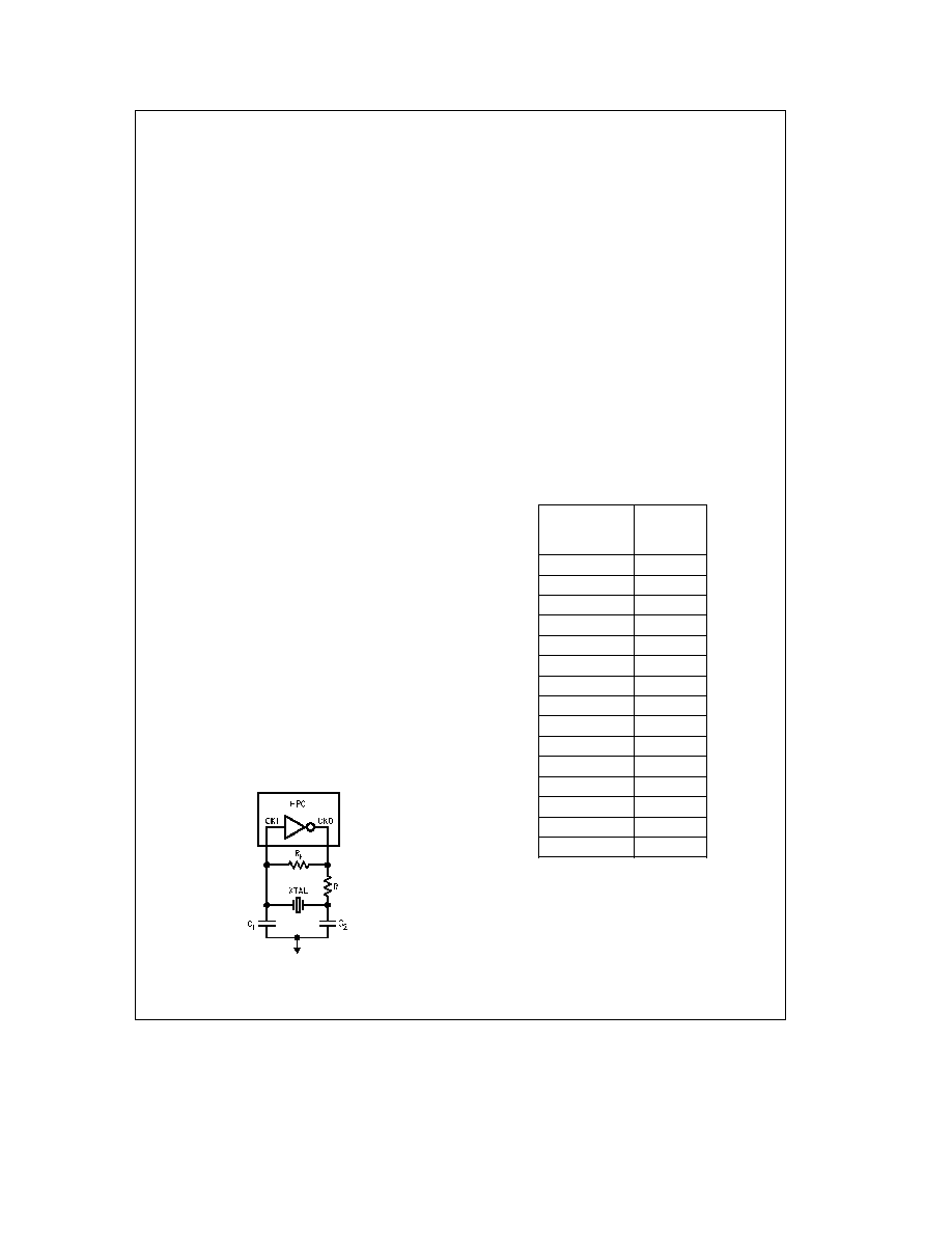
Design Considerations
Designs using the HPC family of 16-bit high speed CMOS
microcontrollers need to follow some general guidelines on
usage and board layout
Floating inputs are a frequently overlooked problem CMOS
inputs have extremely high impedance and if left open can
float to any voltage You should thus tie unused inputs to
V
CC
or ground either through a resistor or directly Unlike
the inputs unused outputs should be left floating to allow
the output to switch without drawing any DC current
To reduce voltage transients keep the supply line's parasit-
ic inductances as low as possible by reducing trace lengths
using wide traces ground planes and by decoupling the
supply with bypass capacitors In order to prevent additional
voltage spiking this local bypass capacitor must exhibit low
inductive reactance You should therefore use high frequen-
cy ceramic capacitors and place them very near the IC to
minimize wiring inductance
Keep V
CC
bus routing short When using double sided or
multilayer circuit boards use ground plane techniques
Keep ground lines short and on PC boards make them
as wide as possible even if trace width varies Use sepa-
rate ground traces to supply high current devices such as
relay and transmission line drivers
In systems mixing linear and logic functions and where
supply noise is critical to the analog components' per-
formance provide separate supply buses or even sepa-
rate supplies
If you use local regulators bypass their inputs with a tan-
talum capacitor of at least 1 mF and bypass their outputs
with a 10 mF to 50 mF tantalum or aluminum electrolytic
capacitor
If the system uses a centralized regulated power supply
use a 10 mF to 20 mF tantalum electrolytic capacitor or a
50 mF to 100 mF aluminum electrolytic capacitor to de-
couple the V
CC
bus connected to the circuit board
Provide localized decoupling For random logic a rule of
thumb dictates approximately 10 nF (spaced within
12 cm) per every two to five packages and 100 nF for
every 10 packages You can group these capacitances
but it's more effective to distribute them among the ICs If
the design has a fair amount of synchronous logic with
outputs that tend to switch simultaneously additional de-
coupling might be advisable Octal flip flop and buffers in
bus-oriented circuits might also require more decoupling
Note that wire-wrapped circuits can require more decou-
pling than ground plane or multilayer PC boards
TL DD 8801 � 40
FIGURE 29 Recommended Crystal Circuit
A recommended crystal oscillator circuit to be used with the
HPC is shown below See table for recommended compo-
nent values The recommended values given in the table
below have yielded consistent results and are made to
match a crystal with a 18 pF load capacitance with some
small allowance for layout capacitance
A recommended layout for the oscillator network should be
as close to the processor as physically possible entirely
within 1
distance This is to reduce lead inductance from
long PC traces as well as interference from other compo-
nents and reduce trace capacitance The layout contains a
large ground plane either on the top or bottom surface of
the board to provide signal shielding and a convenient loca-
tion to ground both the HPC and the case of the crystal
It is very critical to have an extremely clean power supply for
the HPC crystal oscillator Ideally one would like a V
CC
and
ground plane that provide low inductance power lines to the
chip The power planes in the PC board should be decou-
pled with three decoupling capacitors as close to the chip
as possible A 1 0 mF a 0 1 mF and a 0 001 mF dipped mica
or ceramic cap mounted as close to the HPC as is physically
possible on the board using the shortest leads or surface
mount components This should provide a stable power
supply and noiseless ground plane which will vastly im-
prove the performance of the crystal oscillator network
HPC Oscillator Table
XTAL
Frequency
R
1
(X)
(MHz)
s
2
1500
4
1200
6
910
8
750
10
600
12
470
14
390
16
300
18
220
20
180
22
150
24
120
26
100
28
75
30
62
R
F
e
3 3 MX
C
1
e
27 pF
C
2
e
33 pF
XTAL Specifications The crystal used was an M-TRON Industries MP-1 Se-
ries XTAL ``AT'' cut parallel resonant
C
L
e
18 pF
Series Resistance is
25X
25 MHz
40X
10 MHz
600X
2 MHz
27
HPC16083 CPU
The HPC16083 CPU has a 16-bit ALU and six 16-bit regis-
ters
Arithmetic Logic Unit (ALU)
The ALU is 16 bits wide and can do 16-bit add subtract and
shift or logic AND OR and exclusive OR in one timing cycle
The ALU can also output the carry bit to a 1-bit C register
Accumulator (A) Register
The 16-bit A register is the source and destination register
for most I O arithmetic logic and data memory access op-
erations
Address (B and X) Registers
The 16-bit B and X registers can be used for indirect ad-
dressing They can automatically count up or down to se-
quence through data memory
Boundary (K) Register
The 16-bit K register is used to set limits in repetitive loops
of code as register B sequences through data memory
Stack Pointer (SP) Register
The 16-bit SP register is the pointer that addresses the
stack The SP register is incremented by two for each push
or call and decremented by two for each pop or return The
stack can be placed anywhere in user memory and be as
deep as the available memory permits
Program (PC) Register
The 16-bit PC register addresses program memory
Addressing Modes
ADDRESSING MODES
ACCUMULATOR AS
DESTINATION
Register Indirect
This is the ``normal'' mode of addressing for the HPC16083
(instructions are single-byte) The operand is the memory
addressed by the B register (or X register for some instruc-
tions)
Direct
The instruction contains an 8-bit or 16-bit address field that
directly points to the memory for the operand
Indirect
The instruction contains an 8-bit address field The contents
of the WORD addressed points to the memory for the oper-
and
Indexed
The instruction contains an 8-bit address field and an 8- or
16-bit displacement field The contents of the WORD ad-
dressed is added to the displacement to get the address of
the operand
Immediate
The instruction contains an 8-bit or 16-bit immediate field
that is used as the operand
Register Indirect (Auto Increment and Decrement)
The operand is the memory addressed by the X register
This mode automatically increments or decrements the X
register (by 1 for bytes and by 2 for words)
Register Indirect (Auto Increment and Decrement) with
Conditional Skip
The operand is the memory addressed by the B register
This mode automatically increments or decrements the B
register (by 1 for bytes and by 2 for words) The B register is
then compared with the K register A skip condition is gener-
ated if B goes past K
ADDRESSING MODES
DIRECT MEMORY AS
DESTINATION
Direct Memory to Direct Memory
The instruction contains two 8- or 16-bit address fields One
field directly points to the source operand and the other field
directly points to the destination operand
Immediate to Direct Memory
The instruction contains an 8- or 16-bit address field and an
8- or 16-bit immediate field The immediate field is the oper-
and and the direct field is the destination
Double Register Indirect Using the B and X Registers
Used only with Reset Set and IF bit instructions a specific
bit within the 64 kbyte address range is addressed using the
B and X registers The address of a byte of memory is
formed by adding the contents of the B register to the most
significant 13 bits of the X register The specific bit to be
modified or tested within the byte of memory is selected
using the least significant 3 bits of register X
HPC Instruction Set Description
Mnemonic
Description
Action
ARITHMETIC INSTRUCTIONS
ADD
Add
MA
a
MemI
x
MA
carry
x
C
ADC
Add with carry
MA
a
MemI
a
C
x
MA
carry
x
C
ADDS
Add short imm8
MA
a
imm8
x
MA
carry
x
C
DADC
Decimal add with carry
MA
a
MemI
a
C
x
MA (Decimal)
carry
x
C
SUBC
Subtract with carry
MA
b
MemI
a
C
x
MA
carry
x
C
DSUBC
Decimal subtract w carry
MA
b
MemI
a
C
x
MA (Decimal)
carry
x
C
MULT
Multiply (unsigned)
MA MemI
x
MA
X 0
x
K 0
x
C
DIV
Divide (unsigned)
MA MemI
x
MA rem
x
X 0
x
K 0
x
C
DIVD
Divide Double Word (unsigned)
(X
MA) MemI
x
MA rem
x
X 0
x
K carry
x
C
IFEQ
If equal
Compare MA
MemI Do next if equal
IFGT
If greater than
Compare MA
MemI Do next if MA
l
MemI
AND
Logical and
MA and MemI
x
MA
OR
Logical or
MA or MemI
x
MA
XOR
Logical exclusive-or
MA xor MemI
x
MA
MEMORY MODIFY INSTRUCTIONS
INC
Increment
Mem
a
1
x
Mem
DECSZ
Decrement skip if 0
Mem
b
1
x
Mem Skip next if Mem
e
0
28
HPC Instruction Set Description
(Continued)
Mnemonic
Description
Action
BIT INSTRUCTIONS
SBIT
Set bit
1
x
Mem bit
RBIT
Reset bit
0
x
Mem bit
IFBIT
If bit
If Mem bit is true do next instr
MEMORY TRANSFER INSTRUCTIONS
LD
Load
MemI
x
MA
Load incr decr X
Mem(X)
x
A X
g
1 (or 2)
x
X
ST
Store to Memory
A
x
Mem
X
Exchange
A
Mem
Exchange incr decr X
A
Mem(X) X
g
1 (or 2)
x
X
PUSH
Push Memory to Stack
W
x
W(SP) SP
a
2
x
SP
POP
Pop Stack to Memory
SP
b
2
x
SP W(SP)
x
W
LDS
Load A incr decr B
Mem(B)
x
A B
g
1 (or 2)
x
B
Skip on condition
Skip next if B greater less than K
XS
Exchange incr decr B
Mem(B)
A B
g
1 (or 2)
x
B
Skip on condition
Skip next if B greater less than K
REGISTER LOAD IMMEDIATE INSTRUCTIONS
LD B
Load B immediate
imm
x
B
LD K
Load K immediate
imm
x
K
LD X
Load X immediate
imm
x
X
LD BK
Load B and K immediate
imm
x
B imm
x
K
ACCUMULATOR AND C INSTRUCTIONS
CLR A
Clear A
0
x
A
INC A
Increment A
A
a
1
x
A
DEC A
Decrement A
A
b
1
x
A
COMP A
Complement A
1's complement of A
x
A
SWAP A
Swap nibbles of A
A15 12
w
A11 8
w
A7 4
A3 0
RRC A
Rotate A right thru C
C
x
A15
x
x
A0
x
C
RLC A
Rotate A left thru C
C
w
A15
w
w
A0
w
C
SHR A
Shift A right
0
x
A15
x
x
A0
x
C
SHL A
Shift A left
C
w
A15
w
w
A0
w
0
SC
Set C
1
x
C
RC
Reset C
0
x
C
IFC
IF C
Do next if C
e
1
IFNC
IF not C
Do next if C
e
0
TRANSFER OF CONTROL INSTRUCTIONS
JSRP
Jump subroutine from table
PC
x
SP SP
a
2
x
SP
W(table )
x
PC
JSR
Jump subroutine relative
PC
x
SP SP
a
2
x
SP PC
a
x
PC
( is
a
1025 to
b
1023)
JSRL
Jump subroutine long
PC
x
SP SP
a
2
x
SP PC
a
x
PC
JP
Jump relative short
PC
a
x
PC(
is
a
32 to
b
31)
JMP
Jump relative
PC
a
x
PC( is
a
257 to
b
255)
JMPL
Jump relative long
PC
a
x
PC
JID
Jump indirect at PC
a
A
PC
a
A
a
1
x
PC
JIDW
then Mem(PC)
a
PC
x
PC
NOP
No Operation
PC
a
1
x
PC
RET
Return
SP
b
2
x
SP SP
x
PC
RETSK
Return then skip next
SP
b
2
x
SP SP
x
PC
skip
RETI
Return from interrupt
SP
b
2
x
SP SP
x
PC interrupt re-enabled
Note
W is 16-bit word of memory
MA is Accumulator A or direct memory (8 or 16-bit)
Mem is 8-bit byte or 16-bit word of memory
MemI is 8- or 16-bit memory or 8 or 16-bit immediate data
imm is 8-bit or 16-bit immediate data
imm8 is 8-bit immediate data only
29
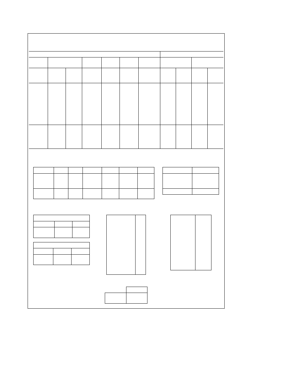
Memory Usage
Number Of Bytes For Each Instruction
(number in parenthesis is 16-Bit field)
Using Accumulator A
To Direct Memory
Reg Indir
Direct
Indir
Index
Immed
Direct
Immed
(B)
(X)
LD
1
1
2(4)
3
4(5)
2(3)
3(5)
5(6)
3(4)
5(6)
X
1
1
2(4)
3
4(5)
ST
1
1
2(4)
3
4(5)
ADC
1
2
3(4)
3
4(5)
4(5)
4(5)
5(6)
4(5)
5(6)
ADDS
2
SBC
1
2
3(4)
3
4(5)
4(5)
4(5)
5(6)
4(5)
5(6)
DADC
1
2
3(4)
3
4(5)
4(5)
4(5)
5(6)
4(5)
5(6)
DSBC
1
2
3(4)
3
4(5)
4(5)
4(5)
5(6)
4(5)
5(6)
ADD
1
2
3(4)
3
4(5)
2(3)
4(5)
5(6)
4(5)
5(6)
MULT
1
2
3(4)
3
4(5)
2(3)
4(5)
5(6)
4(5)
5(6)
DIV
1
2
3(4)
3
4(5)
2(3)
4(5)
5(6)
4(5)
5(6)
DIVD
1
2
3(4)
3
4(5)
4(5)
5(6)
4(5)
5(6)
IFEQ
1
2
3(4)
3
4(5)
2(3)
4(5)
5(6)
4(5)
5(6)
IFGT
1
2
3(4)
3
4(5)
2(3)
4(5)
5(6)
4(5)
5(6)
AND
1
2
3(4)
3
4(5)
2(3)
4(5)
5(6)
4(5)
5(6)
OR
1
2
3(4)
3
4(5)
2(3)
4(5)
5(6)
4(5)
5(6)
XOR
1
2
3(4)
3
4(5)
2(3)
4(5)
5(6)
4(5)
5(6)
8-bit direct address
16-bit direct address
Instructions
that modify memory directly
(B)
(X)
Direct
Indir
Index
B X
SBIT
1
2
3(4)
3
4(5)
1
RBIT
1
2
3(4)
3
4(5)
1
IFBIT
1
2
3(4)
3
4(5)
1
DECSZ
3
2
2(4)
3
4(5)
INC
3
2
2(4)
3
4(5)
Immediate Load Instructions
Immed
LD B
2(3)
LD X
2(3)
LD K
2(3)
LD BK
3(5)
Register Indirect Instructions with
Auto Increment and Decrement
Register B With Skip
(B
a
)
(B
b
)
LDS A
1
1
XS A
1
1
Register X
(X
a
)
(X
b
)
LD A
1
1
X A
1
1
Instructions Using A and C
CLR
A
1
INC
A
1
DEC
A
1
COMP
A
1
SWAP
A
1
RRC
A
1
RLC
A
1
SHR
A
1
SHL
A
1
SC
1
RC
1
IFC
1
IFNC
1
Transfer of Control Instructions
JSRP
1
JSR
2
JSRL
3
JP
1
JMP
2
JMPL
3
JID
1
JIDW
1
NOP
1
RET
1
RETSK
1
RETI
1
Stack Reference Instructions
Direct
PUSH
2
POP
2
30

Code Efficiency
One of the most important criteria of a single chip microcon-
troller is code efficiency The more efficient the code the
more features that can be put on a chip The memory size
on a chip is fixed so if code is not efficient features may
have to be sacrificed or the programmer may have to buy a
larger more expensive version of the chip
The HPC16083 has been designed to be extremely code-
efficient The HPC16083 looks very good in all the standard
coding benchmarks however it is not realistic to rely only
on benchmarks Many large jobs have been programmed
onto the HPC16083 and the code savings over other popu-
lar microcontrollers has been considerable
Reasons for this saving of code include the following
SINGLE BYTE INSTRUCTIONS
The majority of instructions on the HPC16083 are single-
byte There are two especially code-saving instructions
JP is a 1-byte jump True it can only jump within a range of
plus or minus 32 but many loops and decisions are often
within a small range of program memory Most other micros
need 2-byte instructions for any short jumps
JSRP is a 1-byte call subroutine The user makes a table of
the 16 most frequently called subroutines and these calls
will only take one byte Most other micros require two and
even three bytes to call a subroutine The user does not
have to decide which subroutine addresses to put into the
table the assembler can give this information
EFFICIENT SUBROUTINE CALLS
The 2-byte JSR instructions can call any subroutine within
plus or minus 1k of program memory
MULTIFUNCTION INSTRUCTIONS FOR DATA MOVE-
MENT AND PROGRAM LOOPING
The HPC16083 has single-byte instructions that perform
multiple tasks For example the XS instruction will do the
following
1 Exchange A and memory pointed to by the B register
2 Increment or decrement the B register
3 Compare the B register to the K register
4 Generate a conditional skip if B has passed K
The value of this multipurpose instruction becomes evident
when looping through sequential areas of memory and exit-
ing when the loop is finished
BIT MANIPULATION INSTRUCTIONS
Any bit of memory I O or registers can be set reset or
tested by the single byte bit instructions The bits can be
addressed directly or indirectly Since all registers and I O
are mapped into the memory it is very easy to manipulate
specific bits to do efficient control
DECIMAL ADD AND SUBTRACT
This instruction is needed to interface with the decimal user
world
It can handle both 16-bit words and 8-bit bytes
The 16-bit capability saves code since many variables can
be stored as one piece of data and the programmer does
not have to break his data into two bytes Many applications
store most data in 4-digit variables The HPC16083 supplies
8-bit byte capability for 2-digit variables and literal variables
MULTIPLY AND DIVIDE INSTRUCTIONS
The HPC16083 has 16-bit multiply 16-bit by 16-bit divide
and 32-bit by 16-bit divide instructions This saves both
code and time Multiply and divide can use immediate data
or data from memory The ability to multiply and divide by
immediate data saves code since this function is often
needed for scaling base conversion computing indexes of
arrays etc
Development Support
HPC MICROCONTROLLER DEVELOPMENT SYSTEM
National Semiconductor's HPC microcontroller develop-
ment is supported through a combination of third party hard-
ware and software coupled with NSC in-house developed
software consisting of compilers assemblers linkers cross
converters and debuggers The code modules can then be
transferred to many EPROM programming systems
CUSTOMER SUPPORT
National Semiconductor's Customer Response Center
(CRC) provides samples literature prices product informa-
tion The CRC's engineering staff is prepared to answer
questions regarding specific design and application ques-
tions regarding specific design and application questions
Call any weekday 7 00 AM to 7 00 PM central time (US) to
1-800-272-9959 or contact your regional business center
31

Development Support
(Continued)
DIAL-A-HELPER
Dial-A-Helper is a service provided by the Microcontroller
Applications group Dial-A-Helper is an Electronic Bulletin
Board Information system and additionally provides the ca-
pability of remotely accessing the development system at a
customer site
INFORMATION SYSTEM
The Dial-A-Helper system provides access to an automated
information storage and retrieval system that may be ac-
cessed over standard dial-up telephone lines 24 hours a
day The system capabilities include a MESSAGE SECTION
(electronic mail) for communications to and from the Micro-
controller Applications Group and a FILE SECTION which
consists of several file areas where valuable application
software and utilities can be found The minimum require-
ment for accessing Dial-A-Helper is a Hayes compatible mo-
dem
If the user has a PC with a communications package then
files from the FILE SECTION can be down loaded to disk for
later use
Order P N MDS-DIAL-A-HLP
Information system package contains
DIAL-A-HELPER Users Manual
Public Domain Communications Software
FACTORY APPLICATIONS SUPPORT
Dial-A-Helper also provides immediate factory applications
support
Development Tools Selection Table
Order
Description
Manual
Number
Number
NSC
HPC-DEV-IBMA
User's manuals and disks for Assembler Linker Librarian package for the IBM PC
424410836-001
HPC-DEV-IBMC
User's manuals and disks for C Compiler and Assembler Linker Librarian package for the
424410883-001
IBM PC
424410836-001
HPC-DEV-HDB
User's manuals and disks for Source Symbolic Debugger C Compiler and Assembler Linker
424421640-001
Librarian Package for the IBM PC
424410883-001
For use with the HP system only
424410836-001
Signum
USP-HPC
Base Unit
User's manual and screen debugger
POD-HPC164
30 MHz POD and interface board for HPC46164
POD-HPC064
30 MHz POD and interface board for HPC46064
POD-HPC083
30 MHz POD and interface board for HPC46083
POD-HPC100
40 MHz POD and interface board for HPC46100
POD-HPC164-3
20 MHz 3 3V POD and interface board for HPC43164
POD-HPC064-3
20 MHz 3 3V POD and interface board for HPC43064
POD-HPC100-3
30 MHz 3 3V POD and interface board for HPC43100
Hewlett Packard
64700A
Card cage
64706A
48 Channel Analyzer
64775S
Software interface
OPT006
Software interface to IBM PC
64775G
HPC16083 Emulator with 128K RAM
64775H
HPC16064 Emulator with 128K RAM
64775J
HPC16400E Emulator with 128K RAM
64701A
LAN Interface (Optional)
Contact your local NSC sales office for ordering information
The Signum system comes with power supply base unit software RS232 link to host and emulator pod for the HPC Family member
ordered It also includes an interface connector that fits between the POD and the Target board This system does not support
deelopment of HPC46400E based systems Source symbolic debug capability for both assembly and C language is included in the
screen debugger
The HP model 64775 emulator analyzer provides in system emulation up to 20 MHz 0 wait state memory and 30 MHz 1 wait state
memory for al devices except the HPC46400E which is 20 MHz 1 wait state A reverse assembler is also available
The recommended configuration for the IBM PC compatible host is a 386 or higher running DOS 3 0 or higher with 4 MB of
extended memory An RS232 serial port capable of running at 19 2K baud and a three button mouse is recommended for the
Signum System interface
32

Development Support
(Continued)
Voice
(408) 721-5582
Modem (408) 739-1162
Baud 300 or 1200 Baud
Set-Up
Length
8-bit
Parity
None
Stop Bit 1
Operation 24 hrs 7 days
DIAL-A-HELPER
TL DD 8801 � 32
Part Selection
The HPC family includes devices with many different options and configurations to meet various application needs The number
HPC16083 has been generically used throughout this datasheet to represent the whole family of parts The following chart
explains how to order various options available when ordering HPC family members
Note
All options may not currently be available
TL DD 8801 � 31
FIGURE 30 HPC Family Part Numbering Scheme
Examples
HPC46003V20
ROMless Commercial temp (0 C to 70 C) PLCC
HPC16083XXX U20
8k masked ROM Military temp (
b
55 C to
a
125 C) PGA
HPC26083XXX V20
8k masked ROM Automotive temp (
b
40 C to
a
105 C) PLCC
33

Physical Dimensions
inches (millimeters)
Leaded Chip Carrier Package (EL)
Order Number HPC16083XXX L20 HPC16083XXX L30 HPC16003EL20 HPC26003EL20 HPC36003EL20
HPC46003EL20 HPC16003EL30 HPC26003EL30 HPC36003EL30 or HPC46003EL30
NS Package Number EL68A
Pin Grid Array Pinout (U)
Order Number HPC16083XXX U20 HPC16083XXX U30 HPC16003U20 or HPC16003U30
NS Package Number U68A
34
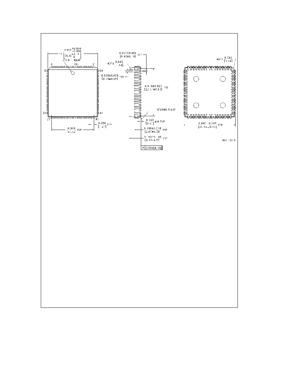
Physical Dimensions
inches (millimeters) (Continued)
Plastic Leaded Chip Carrier (V)
Order Number HPC16083XXX V20 HPC26083XXX V20 HPC36083XXX V20 HPC46083XXX V20 HPC16083XXX V30
HPC26083XXX V30 HPC36083XXX V30 HPC16083XXX V30 HPC16003V20 HPC26003V20 HPC36003V20
HPC46003V20 HPC16003V30 HPC26003V30 HPC36003V30 or HPC46003V30
NS Package Number V68A
35

HPC16083HPC26083HPC36083HPC46083HPC16003HPC26003
HPC36003HPC46003
High-Performance
microControllers
Physical Dimensions
inches (millimeters) (Continued)
80-Pin QFP Package (VF)
Order Number HPC46083XXX F20 HPC46083XXX F30 HPC46003VF20 or HPC46003VF30
NS Package Number VF80B
LIFE SUPPORT POLICY
NATIONAL'S PRODUCTS ARE NOT AUTHORIZED FOR USE AS CRITICAL COMPONENTS IN LIFE SUPPORT
DEVICES OR SYSTEMS WITHOUT THE EXPRESS WRITTEN APPROVAL OF THE PRESIDENT OF NATIONAL
SEMICONDUCTOR CORPORATION As used herein
1 Life support devices or systems are devices or
2 A critical component is any component of a life
systems which (a) are intended for surgical implant
support device or system whose failure to perform can
into the body or (b) support or sustain life and whose
be reasonably expected to cause the failure of the life
failure to perform when properly used in accordance
support device or system or to affect its safety or
with instructions for use provided in the labeling can
effectiveness
be reasonably expected to result in a significant injury
to the user
National Semiconductor
National Semiconductor
National Semiconductor
National Semiconductor
Corporation
Europe
Hong Kong Ltd
Japan Ltd
1111 West Bardin Road
Fax (a49) 0-180-530 85 86
13th Floor Straight Block
Tel 81-043-299-2309
Arlington TX 76017
Email cnjwge tevm2 nsc com
Ocean Centre 5 Canton Rd
Fax 81-043-299-2408
Tel 1(800) 272-9959
Deutsch Tel (a49) 0-180-530 85 85
Tsimshatsui Kowloon
Fax 1(800) 737-7018
English
Tel (a49) 0-180-532 78 32
Hong Kong
Fran ais Tel (a49) 0-180-532 93 58
Tel (852) 2737-1600
Italiano
Tel (a49) 0-180-534 16 80
Fax (852) 2736-9960
National does not assume any responsibility for use of any circuitry described no circuit patent licenses are implied and National reserves the right at any time without notice to change said circuitry and specifications