TL DD11289
HPC46100
High-Performance
microController
with
DSP
Capability
PRELIMINARY
June 1994
HPC46100 High-Performance microController
with DSP Capability
General Description
The HPC46100 is a member of the HPC
TM
family of High
Performance microControllers Each member of the family
has a similar core CPU with unique memory resources and
I O
configuration
to
suit
specific
applications
The
HPC46100 is fabricated in National's advanced microCMOS
technology This process combined with an advanced archi-
tecture provides fast flexible I O control efficient data ma-
nipulation high speed computation and low power con-
sumption
Throughput is enhanced by operating the HPC46100 at fre-
quencies up to 40 MHz by integrating a Multiply Accumu-
late Unit (MAU) onto the chip and by optimizing instructions
to increase efficiency These features increase performance
in closed loop digital servo and filter applications
The HPC devices are complete microcomputers on a single
chip All system timing internal logic RAM and I O are
provided on the chip to produce a cost effective solution
for high performance applications
On-chip functions
such as an MAU unit PWM outputs Chip Select Signals
UART
up to seven 16-bit timers with input capture
capability WATCHDOG
TM
logic vectored interrupts and
MICROWIRE PLUS
TM
provide a high level of system inte-
gration The ability to directly address up to 64 kbytes of
memory enables the HPC to be used in powerful applica-
tions typically performed by microprocessors and peripheral
chips
(Continued)
Features
Y
Multiply Accumulate Unit for fast signed multiply or mul-
tiply-accumulate
Y
High speed 16 bit timers with PWM outputs or input
capture logic
Y
4 Chip select output logic with programmable control
Y
8-channel 8-bit A D Converter
Y
1024 bytes of on-chip 0 wait state RAM
Y
FAST
100
ns
for
fastest
instruction when using
40 0 MHz clock
Y
Very low power with two power save modes IDLE and
HALT
Y
UART full duplex with a programmable baud rate gen-
erator and parity checking detection
Y
MICROWIRE PLUS serial I O interface
Y
8 vectored interrupt sources
Y
Signed overflow flag for add and subtract instructions
Y
16 x 16 multiply and 32 x 16 divide
Y
16-bit architecture with byte and word operations
Y
64 kbytes of direct memory addressing
Y
8- or 16-bit wide external memory
Y
Program instructions can be executed from RAM
Y
Up to 31 general purpose I O lines that are memory
mapped
Y
WATCHDOG logic
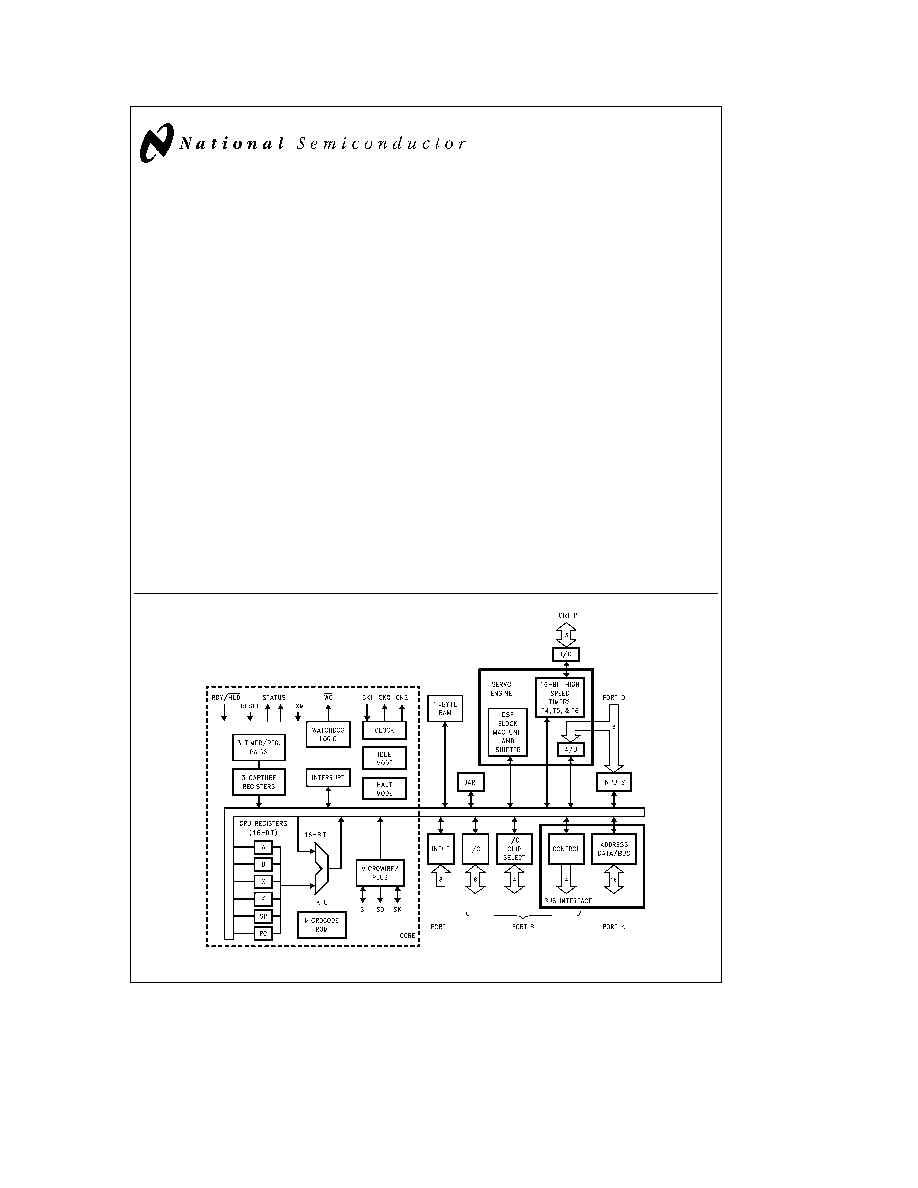
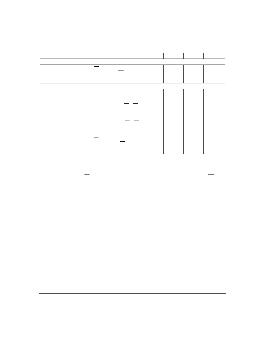
Block Diagram
TL DD 11289 � 1
TRI-STATE
is a registered trademark of National Semiconductor Corporation
HPC
TM
WATCHDOG
TM
MICROWIRE PLUS
TM
and MICROWIRE
TM
are trademarks of National Semiconductor Corporation
C1995 National Semiconductor Corporation
RRD-B30M105 Printed in U S A
General Description
(Continued)
The HPC46100 has as an on-chip peripheral an 8-channel
8-bit Analog-to-Digital Converter This A D converter can
operate in a single-ended mode where the analog input volt-
age is applied across one of the eight input channels (D0 �
D7) and AGND The A D converter can also operate in a
differential mode where the analog input voltage is applied
across two adjacent input channels The A D converter will
convert up to eight channels in the single-ended mode and
up to four channel pairs in the differential mode
A group of three high speed timers provide processor inde-
pendent PWM signal generation These timers and their
support logic provide independent control of PWM frequen-
cy and PWM duty cycle with a minimum resolution of 50 ns
when running at 40 MHz
The HPC46100 is upwards source code compatible with the
HPC family except for Decimal Add and Subtract
The HPC46100 is available in an 80-pin QFP package
40 MHz
Absolute Maximum Ratings
If Military Aerospace specified devices are required
please contact the National Semiconductor Sales
Office Distributors for availability and specifications
Total Allowable Source or Sink Current
100 mA
Storage Temperature Range
b
65 C to
a
150 C
Lead Temperature (Soldering 10 sec )
300 C
V
CC
with Respect to GND
b
0 5V to
a
6 5V
V
REF
with Respect to GND
V
CC
All Other Pins
(V
CC
a
0 5V) to (GND
b
0 5V)
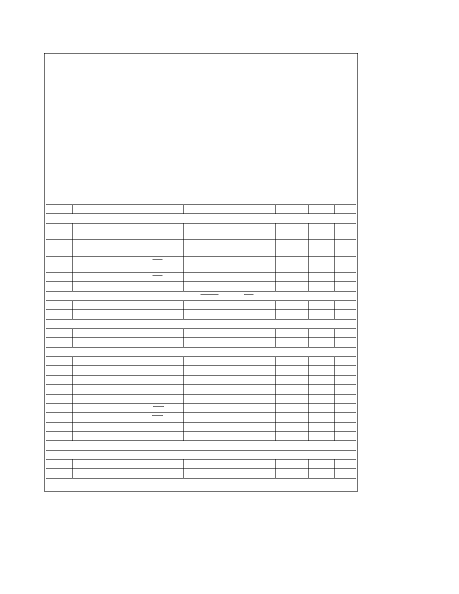
DC Characteristics
V
CC
e
5 0V
g
10% unless otherwise specified T
A
e
0 C to
a
70 C unless otherwise specified
Symbol
Parameter
Test Conditions
Min
Max
Units
SUPPLIES
I
CC1
Supply Current
V
CC
e
5 5V f
IN
e
40 MHz (Note 1)
65
mA
V
CC
e
5 5V f
IN
e
20 MHz (Note 1)
40
mA
I
CC2
IDLE Mode Supply Current
V
CC
e
5 5V f
IN
e
40 MHz (Note 1)
25
mA
V
CC
e
5 5V f
IN
e
20 MHz (Note 1)
20
mA
I
CC3
HALT Mode Supply Current with NMI High
V
CC
e
5 5V f
IN
e
0 (Note 1)
300
m
A
V
CC
e
2 5V f
IN
e
0 (Note 1)
100
m
A
I
CC4
HALT Mode Supply Current with NMI Low
V
CC
e
5 5V f
IN
e
40 MHz (Note 1)
25
mA
V
RAM
RAM Keep-Alive Voltage
(Note 2)
2 5
V
INPUT VOLTAGE LEVELS FOR SCHMITT TRIGGERED INPUTS RESET NMI AND WO AND ALSO CKI
V
IH1
Logic High
0 9 V
CC
V
V
IL1
Logic Low
0 1 V
CC
V
INPUT VOLTAGE LEVELS FOR PORT A
V
IH2
Logic High
2 0
V
V
IL2
Logic Low
0 8
V
INPUT VOLTAGE LEVELS FOR ALL OTHER INPUTS
V
IH3
Logic High (except Port D)
0 7 V
CC
V
V
IL3
Logic Low (except Port D)
0 2 V
CC
V
V
IH4
Logic High (Port D only)
(Note 6 in AC Characteristics)
0 7 V
CC
V
V
IL4
Logic Low (Port D only)
(Note 6 in AC Characteristics)
0 2 V
CC
V
I
LI1
Input Leakage Current all pins except below
10
m
A
I
LI2
Input Leakage Current pin RDY HLD only
b
3
b
50
m
A
I
LI3
Input Leakage Current pin B12 (HBE) only
RESET
e
GND V
IN
e
V
CC
0 5
7 0
mA
C
I
Input Pin Capacitance
(Note 3)
10
pF
C
IO
Input Output Pin Capacitance
(Note 3)
20
pF
OUTPUT VOLTAGE LEVELS
CMOS USAGE ALL OUTPUTS AND I O PINS
V
OH1
Logic High
I
OH
e b
10 mA (Note 3)
V
CC
b
0 1
V
V
OL1
Logic Low
I
OL
e
10 mA (Note 3)
0 1
V
2
40 MHz
(Continued)
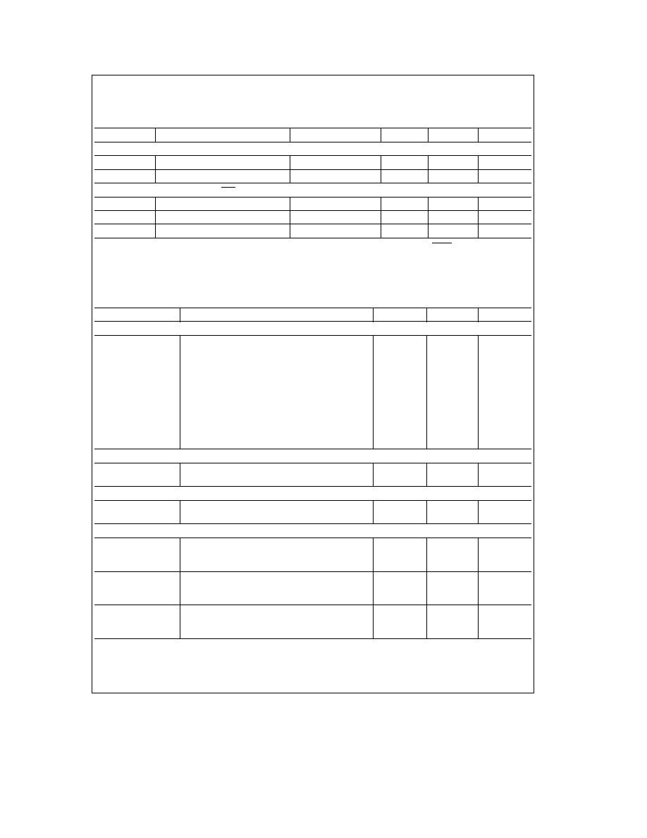
DC Characteristics
V
CC
e
5 0V
g
10% unless otherwise specified T
A
e
0 C to
a
70 C unless otherwise specified (Continued)
Symbol
Parameter
Test Conditions
Min
Max
Units
BUS DRIVERS PORT A AND PINS B8 � B15 PALE CK2 ST1 AND ST2
V
OH2
Logic High
I
OH
e b
1 mA
2 4
V
V
OL2
Logic Low
I
OL
e
3 mA
0 4
V
OTHER I O PORT DRIVERS B0 � B7 WO P0 � P2
V
OH3
Logic High
I
OH
e b
1 6 mA
2 4
V
V
OL3
Logic Low
I
OL
e
0 5 mA
0 4
V
I
OZ
TRI-STATE Leakage Current
10
m
A
Note 1
I
CC1
I
CC2
I
CC3
and I
CC4
are measured with no external drive (I
OH
and I
OL
e
0 I
IH
and I
IL
e
0) I
CC1
is measured with RESET
e
GND I
CC3
is measured
with NMI
e
V
CC
I
CC4
is measured with NMI
e
GND CKI driven to V
IH1
and V
IL1
with rise and fall times less than 10 ns
Note 2
Test duration is 100 ms
Note 3
This is guaranteed by design and not tested
AC Electrical Characteristics
See Notes 1 and 4 and
Figure 1 thru Figure 5 V
CC
e
5 0V
g
10% unless otherwise specified T
A
e
25 C one wait state
Symbol
Parameter
Min
Max
Units
CLOCKS
f
C
CKI Operating Frequency
2
40
MHz
t
C1
e
1 f
C
CKI Period
25
500
ns
t
C1H
CKI High Time
11 25
ns
t
C1L
CKI Low Time
11 25
ns
t
C
e
2 f
C
Bus Timing Cycle
50
1000
ns
t
WAIT
Wait State Period
50
ns
t
DC1C2R
CK2 Rising Edge after CKI Falling Edge (Note 2)
0
55
ns
t
DC1C2F
CK2 Falling Edge after CKI Falling Edge (Note 2)
0
55
ns
f
U
External UART Clock Input Frequency
5
MHz
f
MW
External MICROWIRE PLUS Clock
2 5
MHz
Input Frequency
TIMER T0 � T3
f
XIN
e
f
C
22
External Timer Input Frequency
1 82
MHz
t
XIN
e
t
C
Pulse Width for Timer Input
50
ns
TIMER T4 � T6
f
HSXIN
e
f
C
5
External Timer Input Frequency
8
MHz
t
HSXIN
e
1 5 t
C
Pulse Width for Timer Input
75
ns
MICROWIRE PLUS
t
UWS
MICROWIRE Setup Time
Master
100
ns
Slave
20
t
UWH
MICROWIRE Hold Time
Master
20
ns
Slave
50
t
UWS
MICROWIRE Output Valid Time
Master
50
ns
Slave
150
3
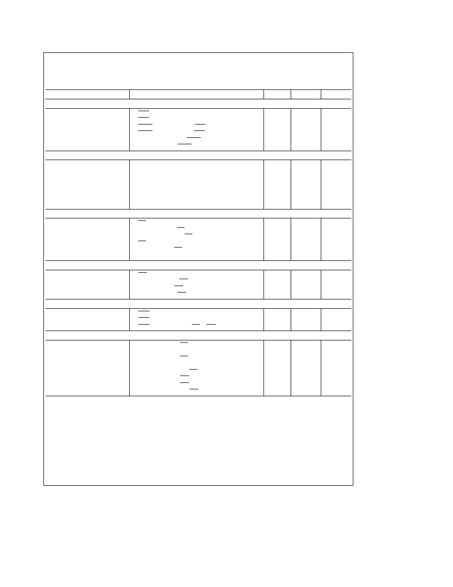
40 MHz
(Continued)
AC Electrical Characteristics
(Continued)
See Notes 1 and 4 and
Figure 1 thru Figure 5 ) V
CC
e
5 0V
g
10% unless otherwise specified T
A
e
25 C one wait state
Symbol
Parameter
Min
Max
Units
EXTERNAL HOLD
t
SALE
e
0 75 t
C
a
40
HLD Falling Edge before ALE Rising Edge
77 5
ns
t
HWP
e
0 75 t
C
a
35
HLD Pulse Width
72 5
ns
t
HAE
e
0 75 t
C
a
100
HLDA Falling Edge after HLD Falling Edge (Note 3)
137 5
ns
t
HAD
e
0 75 t
C
a
85
HLDA Rising Edge after HLD Rising Edge
122 5
ns
t
BF
Bus TRI-Stated after HLDA Falling Edge (Note 5)
70
ns
t
BE
e
0 75 t
C
a
30
Bus Enable after HLDA Rising Edge
67 5
ns
NATIVE BUS TIMING ADDRESS CYCLE
t
LL
e
0 5 t
C
b
10
ALE Pulse Width
15
ns
t
1ALR
ALE Rising Edge after CK1 Rising Edge (Note 2)
0
35
ns
t
1ALF
ALE Falling Edge after CK1 Falling Edge (Note 2)
0
35
ns
t
2ALR
e
0 25 t
C
a
20
ALE Rising Edge after CK2 Rising Edge
32 5
ns
t
2ALF
e
0 25 t
C
a
20
ALE Falling Edge after CK2 Falling Edge
32 5
ns
t
ST
e
0 25 t
C
b
9
Address Valid to ALE Falling Edge
3 5
ns
t
VP
e
0 5 t
C
b
10
Address Hold after ALE Falling Edge
15
ns
READ CYCLE
t
RW
e
0 25 t
C
a
WS
b
15
RD Pulse Width
47 5
ns
t
ARD
e
0 75 t
C
b
20
Address Valid to RD Falling Edge
17 5
ns
t
ARR
e
0 5 t
C
b
20
ALE Falling Edge to RD Falling Edge
5
ns
t
RD
e
0 25 t
C
a
WS
b
20
RD Falling Edge to Input Data Valid
42 5
ns
t
DR
Data Hold after RD Rising Edge
0
50
ns
t
ACC
e
t
C
a
WS
b
20
Address Valid to Input Data Valid
80
ns
WRITE CYCLE
t
WW
e
0 75 t
C
a
WS
b
15
WR Pulse Width
72 5
ns
t
V
e
0 5 t
C
a
WS
b
20
Data Valid before WR Rising Edge
55
ns
t
HW
e
0 5 t
C
b
10
Data Hold after WR Rising Edge
15
ns
t
AWR
e
0 75 t
C
b
20
Address Valid to WR Falling Edge
17 5
ns
READY INPUT
t
RDYS
RDY Falling Edge before CK2 Falling Edge
45
ns
t
RDYH
RDY Rising Edge after CK2 Falling Edge
0
ns
t
RDYV
e
WS
a
0 25 t
C
b
30
RDY Falling Edge after RD or WR Falling Edge
32 5
ns
CHIP SELECT NATIVE BUS TIMING
t
CS30RD
e
0 75 t
C
b
30
CS3 CS0 Valid to RD Falling Edge
7 5
ns
t
ACCS30
e
t
C
a
WS
b
30
CS3 CS0 Valid to Input Data Valid
70
ns
t
CS21RD
e
0 75 t
C
b
35
CS2 CS1 Valid to RD Falling Edge
2 5
ns
t
ACCS21
e
t
C
a
WS
b
35
CS2 CS1 Valid to Input Data Valid
65
ns
t
CSHR
e
t
C
b
15
Chip Select Hold after RD Rising Edge
35
ns
t
CS30WR
e
0 75 t
C
b
30
CS3 CS0 Valid to WR Falling Edge
7 5
ns
t
CS21WR
e
0 75 t
C
b
35
CS2 CS1 Valid to WR Falling Edge
2 5
ns
t
CSHW
e
0 5 t
C
b
15
Chip Select Hold after WR Rising Edge
10
ns
4
40 MHz
(Continued)
AC Electrical Characteristics
(Continued)
See Notes 1 and 4 and
Figure 1 thru Figure 5 V
CC
e
5 0V
g
10% unless otherwise specified T
A
e
25 C one wait state
Symbol
Parameter
Min
Max
Units
E SIGNAL TIMING PARAMETERS
t
RWSE
e
0 25 t
C
b
7
WR Falling Edge to E Rising Edge
5 5
ns
t
RWHE
e
0 5 t
C
b
7
E Falling Edge to WR Rising Edge
18
ns
t
ASE
e
t
C
b
20
Address Valid to E Rising Edge
30
ns
t
RDE
e
WS
b
20
E Falling Edge to Data Input Valid
30
ns
SLOW PERIPHERAL TIMING PARAMETERS
t
PLL
e
t
C
b
5
PALE Pulse Width
45
ns
t
PST
e
0 75 t
C
b
10
Address Valid to PALE Falling Edge
27 5
ns
t
PVL
e
0 75 t
C
b
15
Address Hold from PALE Falling Edge
22 5
ns
t
PVP
e
0 75 t
C
b
10
PALE Falling Edge to RD or WR Falling Edge
27 5
ns
t
PCSA
e
0 25 t
C
b
12 5
Chip Select Setup to PALE Falling Edge
0
ns
t
PAS
e
1 5 t
C
b
20
Address Setup to RD or WR Falling Edge
55
ns
t
PCSS
e
t
C
b
15
Chip Select Setup to RD or WR Falling Edge
35
ns
t
PCSH
e
0 5 t
C
b
15
Chip Select Hold from RD or WR Rising Edge
10
ns
t
PACC
e
5 t
C
b
25
Address Valid to Input Data Valid
225
ns
t
PRD
e
3 5 t
C
b
25
RD Falling Edge to Data In Valid
150
ns
t
PDR
e
t
C
(max)
Data Hold after RD Rising Edge
0
50
ns
t
PRW
e
3 5 t
C
b
15
RD Strobe Width
160
ns
t
PSW
e
3 0 t
C
b
20
Data Setup before WR Rising Edge
130
ns
t
PHW
e
t
C
b
20
Data Hold after WR Rising Edge
30
ns
t
PWW
e
3 5 t
C
b
15
WR Strobe Width
160
ns
Note
C
L
e
40 pF
Note 1
These AC characteristics are guaranteed with external clock drive on CKI having 50% duty cycle and with less than 15 pF load on CKO with rise and fall
times (t
CKIR
and t
CKIL
) on CKI input less than 2 5 ns
Note 2
Do not design with these parameters unless CKI is driven with an active signal When using a passive crystal circuit its stability is not guaranteed if either
CKI or CKO is connected to any external logic other than the passive components of the crystal circuit
Note 3
t
HAE
is spec'd for case with HLD falling edge occurring at the latest time it can be accepted during the present CPU cycle begin executed If HLD falling
edge occurs later t
HAE
as long as (3 t
C
a
4 WS
a
72 t
C
a
100) may occur depending on the following CPU instruction cycles its wait states and ready input
Note 4
WS (t
WAIT
) x (number of preprogrammed wait states) Minimum and maximum values are calculated at maximum operating frequency t
C
e
40 MHz with
one wait state programmed
Note 5
Due to testing limitations
actual limits will be better
5