TL DD11727
ICSS1001
ICSS1002
and
ICSS1003
ICSS
Power
Line
Carrier
Local
Area
Network
Chip
Set
PRELIMINARY
February 1995
ICSS1001 ICSS1002 and ICSS1003
IC SS Power Line Carrier
Local Area Network Chip Set
General Description
Integrated Circuit Spread Spectrum (IC SS
TM
) is a power
line carrier local area network system implemented in a
three chip solution using power line carrier technology de-
veloped by Itron and Cyplex It is designed to operate with
high reliability over the full range of power line conditions
IC SS is offered with an integral local area network proto-
col designed specifically for supervisory control and data
acquisition applications
Features
Y
Spread spectrum adaptive frequency hopping modula-
tion provides high immunity to power line noise
Y
Network transparent option offers the user the ability to
carry proprietary protocols transparently or to use the
built-in link layer protocol
Y
A very flexible interface to the user's circuit is provided
configurable either to accept serial data or to accept
data from an 8-bit parallel bus Handshake lines are
provided to facilitate interface to common microproces-
sors in parallel mode
Y
When used with the specified coupling networks the
modem
operates
in
conformance
with
both
the
CENELEC
standard
for
electric
utility
application
(9 kHz � 95 kHz) and with FCC Class A requirements
Y
Data rate is variable based on line conditions from
300 bps to 3200 bps
Y
When used with the specified coupling networks the
system provides 93 dB of dynamic range appropriate
for line loading and attenuation effects common on
power lines
Y
The modem's bit error rate performance in additive
white noise approaches the theoretical maximum and
in addition it provides excellent immunity to the impul-
sive noise characteristic of power lines
Applications
Y
Automated meter reading (AMR)
Y
Demand side management
Y
Distribution automation
Y
Environmental control systems
Y
Other power line carrier applications requiring high
reliability
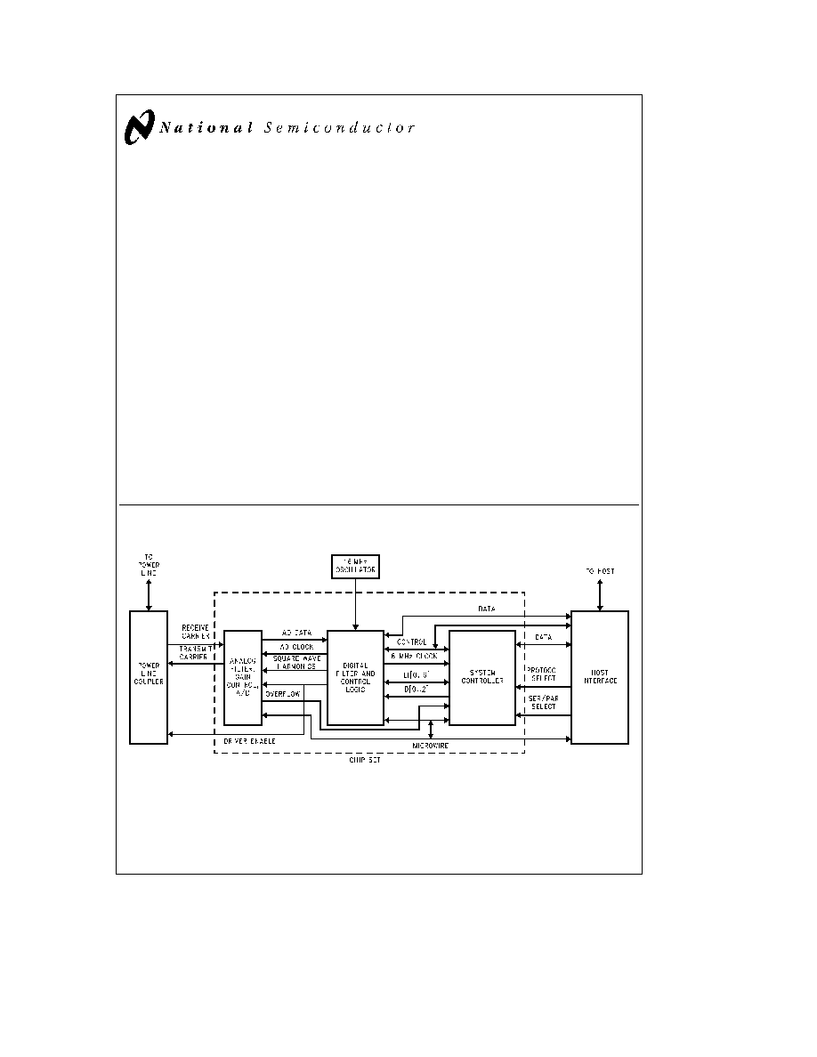
Block Diagram
TL DD 11727 � 1
TRI-STATE
is a registered trademark of National Semiconductor Corporation
MICROWIRE
TM
and WATCHDOG
TM
are trademarks of National Semiconductor Corporation
IC SS
TM
is a trademark of Cyplex
C1995 National Semiconductor Corporation
RRD-B30M105 Printed in U S A
Modem Operation
A block diagram of the modem is shown on page 1 It in-
cludes four major elements
1 Coupling network to the power line
2 Analog filter gain control and A D
3 Digital filter and control logic
4 System controller
Each of these is described in more detail below
COUPLING NETWORK
The coupling network provides protection against the AC
power line 60 Hz 50 Hz energy and initial filtering of power
line noise It provides a match of impedances to the power
line and also contains a power amplification stage for the
transmitter A variety of coupling networks are available
from Cyplex suitable for
220 VAC ungrounded operation (meters and 220 VAC
load control)
110 VAC neutral operation (110 VAC load control)
Three-terminal operation (intended for gateways and
master units which must communicate with both of the
above)
The coupling networks require
g
5V power ground and in-
terface to the analog section of the system
ICSS1001
Controller
The controller provides the adaptive frequency hopping the
user interface and link layer protocol
ICSS1002
Digital Chip
The digital section of the system provides additional receive
filtering and received signal detection functions It generates
the necessary internal clocks and interface signals to the
microcontroller
ICSS1003
Analog Chip
The analog section of the system provides receive signal
filtering and also generates the transmit carrier based on
control and clock signals from the digital section
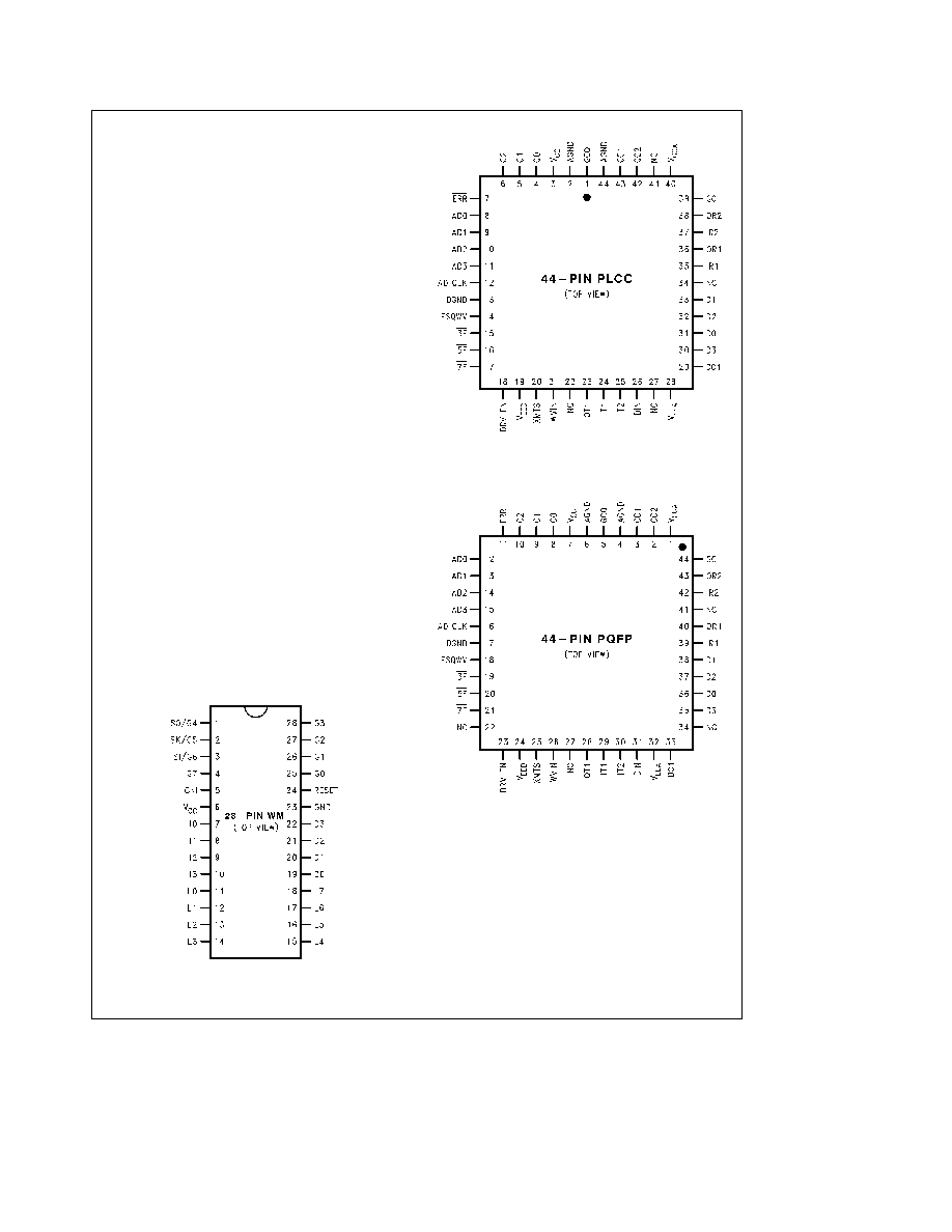
Connection Diagrams
TL DD 11727 � 2
Wide Molded Small Outline Package (WM)
Order Number ICSS1001WM
NS Package Number M28B
TL DD 11727 � 4
Plastic Leaded Chip Carrier (PLCC)
Order Number ICSS1003V
NS Package Number V44A
TL DD 11727 � 28
Plastic Quad Flatpak (PQFP)
Order Number ICSS1003VGZ
NS Package Number VGZ44A
2
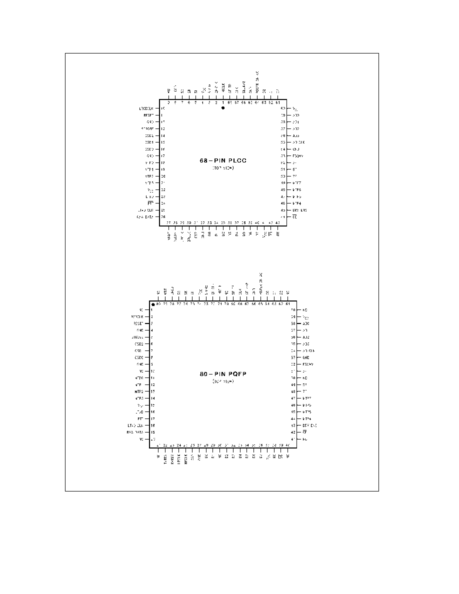
Connection Diagrams
(Continued)
TL DD 11727 � 3
Plastic Leaded Chip Carrier (PLCC)
Order Number ICSS1002V4
NS Package Number V68A
TL DD 11727 � 27
Plastic Quad Flatpak (PQFP)
Order Number ICSS1002VJE
NS Package Number VJE80B
3

Pin Descriptions
Tables I II and III describe the various pins that are used for
external connections outside of the chip set These pins are
shown in the Connection Diagrams
Type
One of the following
I
Input
O
Output
T
TRI-STATE
P
Power
Function
A brief description of each signal's function
TABLE I ICSS1001 Pin Descriptions
Pin Name
Pin No
Type
Function
SO G4
1
O
MICROWIRE
TM
SO to digital ASIC
SK G5
2
O
MICROWIRE clock to digital ASIC
SI G6
3
I
MICROWIRE SI from digital ASIC
G7
4
O
Overflow of A D converter from analog ASIC
CKI
5
l
8 MHz clock input from digital ASIC
V
CC
6
P
Input power
I0
7
I
RAW DATA input from digital ASIC
I1
8
O
RxRDY handshake line for parallel port
I2
9
I
SER PAR-input read after reset determines whether firmware will use serial or parallel host
port HIGH
e
serial
I3
10
I
NET TRN-input read continuously If HIGH and serial port is selected commands are
processed if LOW all received characters are treated as transparent data If parallel port is
selected this pin has no effect
L0
11
I
RTS flow control from host If serial port is selected (pin 9
e
HIGH) LOW enables output of
data on RCD and HIGH prevents output on RCD A byte in the process of being output when
RTS goes HIGH will be completed RTS has no effect if parallel port is selected
If parallel is selected (pin 9
e
LOW) COMMAND HIGH denotes the presence of a command
in the parallel port input buffer LOW denotes the presence of data
L1
12
O
CTS flow control to host Normally LOW If serial port is selected (pin 9
e
HIGH) then HIGH
indicates host should not send data to TXD A maximum of three bytes will be accepted after a
transition from LOW to HIGH
If parallel port is selected (pin 9
e
LOW) then STATUS HIGH denotes that the byte available
for the host to read is a status code A LOW denotes that the available byte is data
L2
13
O
RCD receive data output to host in byte asynchronous format 8 data bits parity one start and
one stop bit Active baud rate and parity default is 1200 baud no parity Other settings may be
selected by DIP switch Active only if serial port is selected
L3
14
I
TXD transmit data input from host
L4
15
O
LTXD CLK serial data clock for data to be transmitted by the digital ASIC not Manchester-
encoded
L5
16
O
TxRDY handshake line for parallel port
L6
17
O
PTT Active LOW places digital chip in transmit mode
L7
18
O
LTXD serial data to be transmitted by digital ASIC not Manchester-encoded Active HIGH
ASIC Manchester-encodes the data using LTXD CLK
D0
19
O
CSD digital ASIC internal MlCROWIRE register address selection
D1
20
O
CSD1 digital ASIC internal MlCROWIRE register address selection
D2
21
O
CSD2 digital ASIC internal MICROWIRE register address selection
D3
22
O
STROBE MICROWIRE output to digital ASIC
GROUND
23
P
Ground
RESET
24
I
RESET from digital chip
4
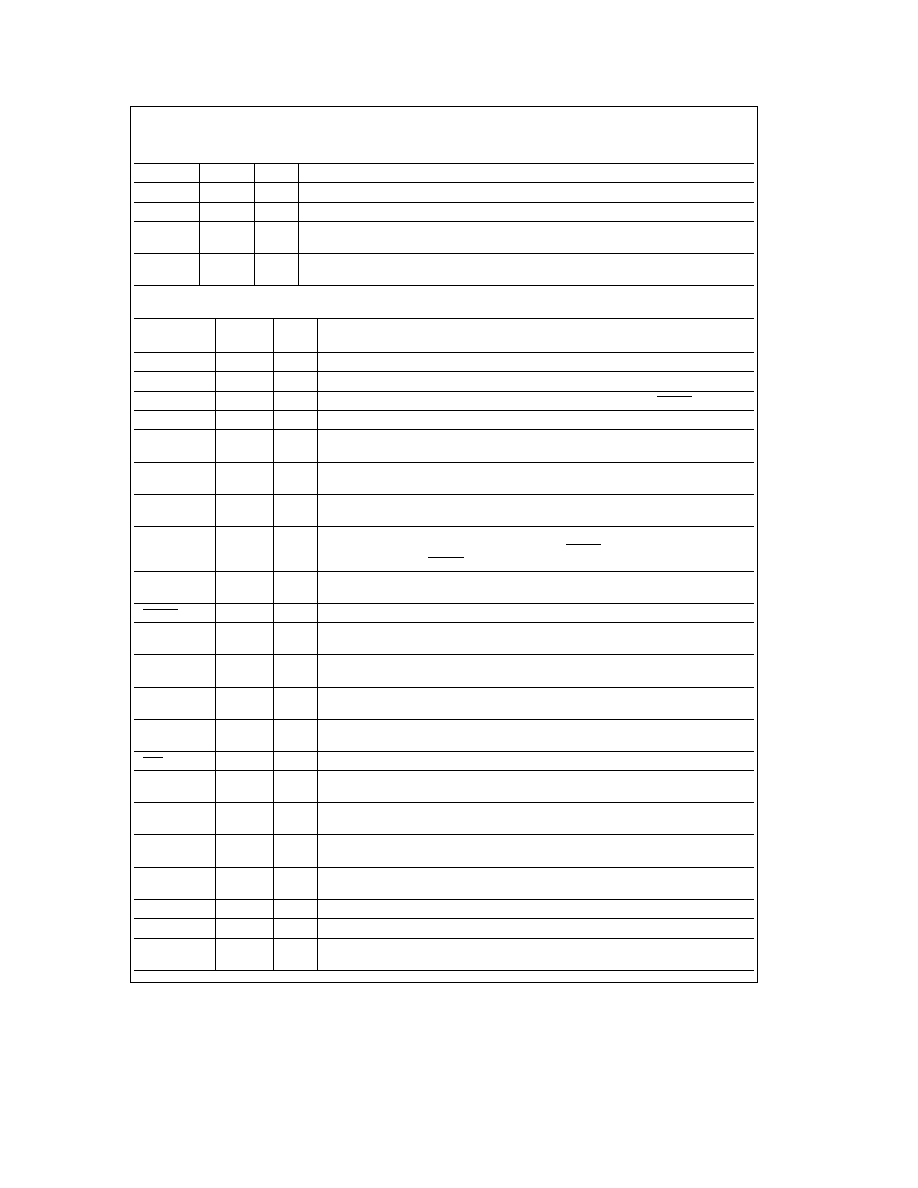
Pin Descriptions
(Continued)
TABLE I ICSS1001 Pin Descriptions
(Continued)
Pin Name
Pin No
Type
Function
G0
25
I
LRCD CLK recovered clock from demodulated data input from digital ASlC
G1
26
No connection
G2
27
I
LRCD recovered data from demodulated data input from digital ASIC after Manchester
decoding
G3
28
O
WDT firmware outputs a square wave to digital chip maintaining a one-shot If WDT output
stops digital ASIC will force a system reset on pin 24
TABLE II ICSS1002 Pin Descriptions
Pin Name
Pin No
Type
Function
(V Pkg )
IHICLK
1
O
Output Test Point
A test point
QHICLK
2
O
Output Test Point
A test point
8 MHz
3
O
8 MHz Output
This is the CLK divided by 2 This output goes low while RESET is LOW
SI
5
T
MICROWIRE Serial Input
This pin drives the MICROWIRE SI Input on the controller
SK
6
T
MICROWIRE Shift Clock
This pin accepts the MICROWIRE shift clock to the Controller
interface on the IC SS digital ASIC
SO
7
T
MICROWIRE Serial Output
This pin accepts the MICROWIRE serial data to the
Controller interface on the IC SS digital ASIC
LRCD
8
O
Recovered Data
This is the serial data received from the power line after Manchester
decoding
WDT
9
T
WATCHDOG
TM
Timer Disable
This input from the controller keeps the digital ASIC
active If it goes away the digital ASlC will generate RESET pulse after the WATCHDOG
timers times out This RESET pulse will reset the entire PLC chip set
LRCDCLK
10
O
Recovered Clock
This is the clock received from the power line after Manchester
decoding
RESET
11
I
Reset
Active LOW reset for the entire IC SS chip set
STROBE
13
T
MICROWIRE Strobe input
This pin accepts the MICROWIRE strobe to the controller
interface on the IC SS digital ASIC
CSD2 � CSD0
14 � 16
T
Controller Interface Mode Select
These inputs are used to select the operation modes
of the controller interface circuitry on the IC SS digital ASIC
MTP0 � MTP3
18 � 21
O
Test Points
These output pins provide access to one of the filter outputs on the detector
integration bus
LTXD
23
O
Serial Data to be transmitted
This input is the serial data to be transmitted It is not
Manchester encoded
PTT
24
T
Push to talk
This is an active low signal that puts the digital ASIC into the transmit mode
LTXD CLK
25
T
Serial Data Transmit Clock
This input is the clock for the serial data (LTXD) that is used
to Manchester encode the data prior to transmission
RAW DATA
26
O
Raw Data
This output is the raw data received by the IC SS circuit after de-multiplex prior
to Manchester decode
TxRDY
27
O
Transmit Data Ready
When this signal is HIGH the parallel port is ready to accept a new
byte from the user data bus
RxRDY
28
O
Receive Data Ready
When this signal is HIGH there is a byte available in the parallel
port to be read by the user data bus
LPCLK
29
O
LPCLK
This is an internal test point
BPCLK
30
O
BPCLK
This is an internal test point
CS2
31
O
Chip Select
This is the MICROWIRE chip select output It is used to enable read write of
external MICROWIRE data ports
5