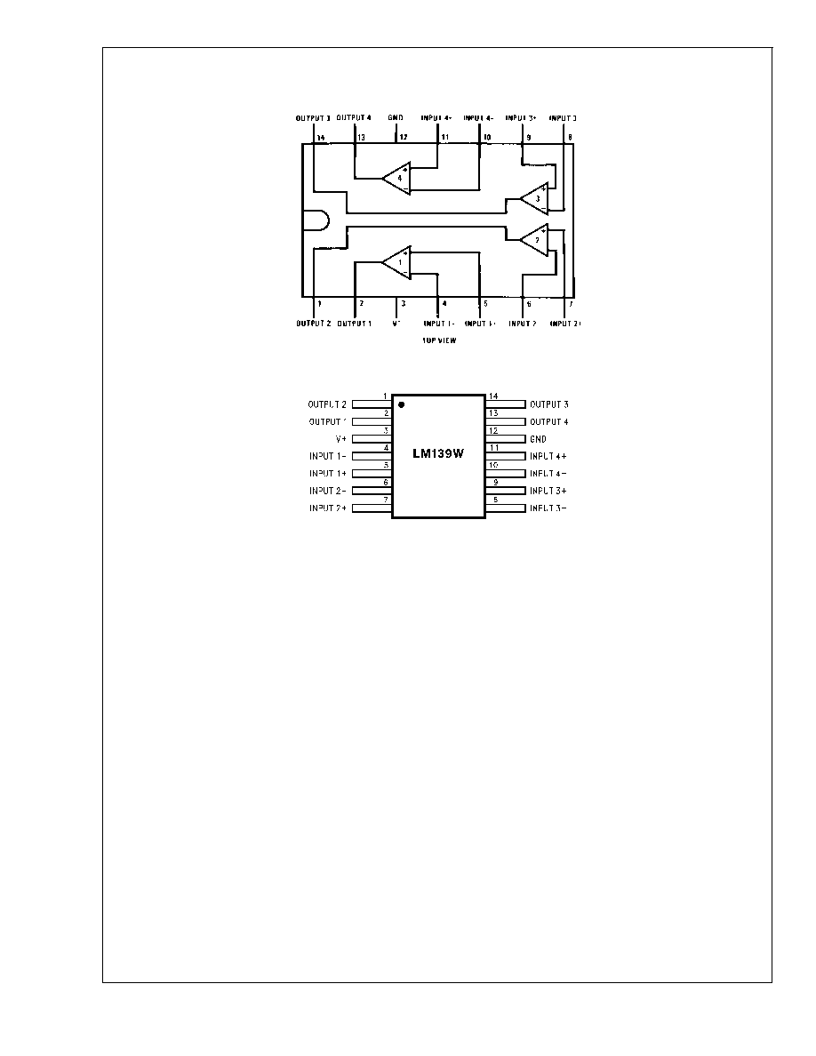
LM139JAN
Low Power Low Offset Voltage Quad Comparators
General Description
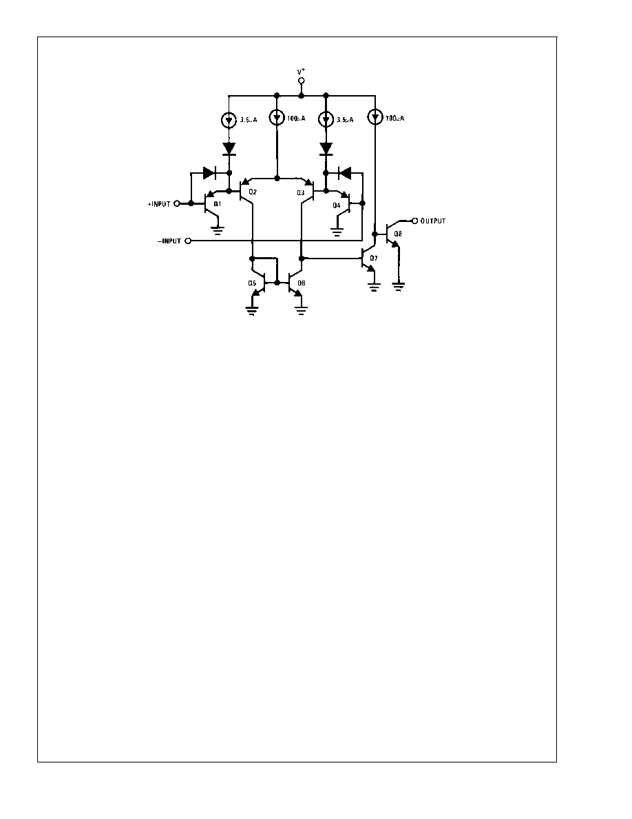
The LM139 consists of four independent precision voltage
comparators with an offset voltage specification as low as 2
mV max for all four comparators. These were designed
specifically to operate from a single power supply over a
wide range of voltages. Operation from split power supplies
is also possible and the low power supply current drain is
independent of the magnitude of the power supply voltage.
These comparators also have a unique characteristic in that
the input common-mode voltage range includes ground,
even though operated from a single power supply voltage.
Application areas include limit comparators, simple analog to
digital converters; pulse, squarewave and time delay gen-
erators; wide range VCO; MOS clock timers; multivibrators
and high voltage digital logic gates. The LM139 was de-
signed to directly interface with TTL and CMOS. When op-
erated from both plus and minus power supplies, they will
directly interface with MOS logic -- where the low power
drain of the LM139 is a distinct advantage over standard
comparators.
Features
n
Wide supply voltage range
5V to 36 V
DC
or
±
2.5V to
±
18 V
DC
n
Very low supply current drain (0.8 mA) -- independent
of supply voltage
n
Low input biasing current:
25 nA
n
Low input offset current:
±
5 nA
n
Offset voltage:
±
3 mV
n
Input common-mode voltage range includes GND
n
Differential input voltage range equal to the power
supply voltage
n
Low output saturation voltage:
250 mV at 4 mA
n
Output voltage compatible with TTL, DTL, ECL, MOS
and CMOS logic systems
Advantages
n
High precision comparators
n
Reduced V
OS
drift over temperature
n
Eliminates need for dual supplies
n
Allows sensing near GND
n
Compatible with all forms of logic
n
Power drain suitable for battery operation
Ordering Information
NS Part Number
JAN Part Number
NS Package Number
Package Description
JL139BCA
JM38510/11201BCA
J14A
14LD CERDIP
JL139SCA
JM38510/11201SCA
J14A
14LD CERDIP
JL139BZA
JM38510/11201BZA
WG14A
14LD Ceramic SOIC
JL139SZA
JM38510/11201SZA
WG14A
14LD Ceramic SOIC
JL139BDA
JM38510/11201BDA
W14B
14LD CERPACK
JL139SDA
JM38510/11201SDA
W14B
14LD CERPACK
February 2005
LM139JAN
Low
Power
Low
Offset
V
oltage
Quad
Comparators
© 2005 National Semiconductor Corporation
DS201295
www.national.com
Absolute Maximum Ratings
(Note 1)
Supply Voltage, V
+
36 V
DC
or
±
18 V
DC
Differential Input Voltage (Note 7)
36 V
DC
Output Voltage
36 V
DC
Input Voltage
-0.3 V
DC
to +36 V
DC
Input Current (V
IN
<
-0.3 V
DC
) (Note 3)
50 mA
Power Dissipation
(Notes 4, 12)
CERDIP
400 mW
@
T
A
= 125°C
CERPACK
350 mW
@
T
A
= 125°C
SOIC
350 mW
@
T
A
= 125°C
Output Short-Circuit to GND,
(Note 2)
Continuous
Storage Temperature Range
-65°C
T
A
+150°C
Maximum Junction Temperature (T
J
)
+175°C
Lead Temperature
(Soldering, 10 seconds)
260°C
Operating Temperature Range
-55°C
T
A
+125°C
Thermal Resistance
JA
CERDIP
(Still Air)
103°C/W
CERDIP
(500LF / Min Air flow)
65°C/W
CERPACK
(Still Air)
183°C/W
CERPACK
(500LF / Min Air flow)
120°C/W
SOIC
(Still Air)
183°C/W
SOIC
(500LF / Min Air flow)
120°C/W
JC
CERDIP
23°C/W
CERPACK
23°C/W
SOIC
23°C/W
Package Weight (typical)
CERDIP
2,190mg
CERPACK
460mg
SOIC
410mg
ESD rating
(Note 11)
600V
Quality Conformance Inspection
Mil-Std-883, Method 5005 -- Group A
Subgroup
Description
Temp (°C)
1
Static tests at
25
2
Static tests at
125
3
Static tests at
-55
4
Dynamic tests at
25
5
Dynamic tests at
125
6
Dynamic tests at
-55
7
Functional tests at
25
8A
Functional tests at
125
8B
Functional tests at
-55
9
Switching tests at
25
10
Switching tests at
125
11
Switching tests at
-55
LM139JAN
www.national.com
4
LM139
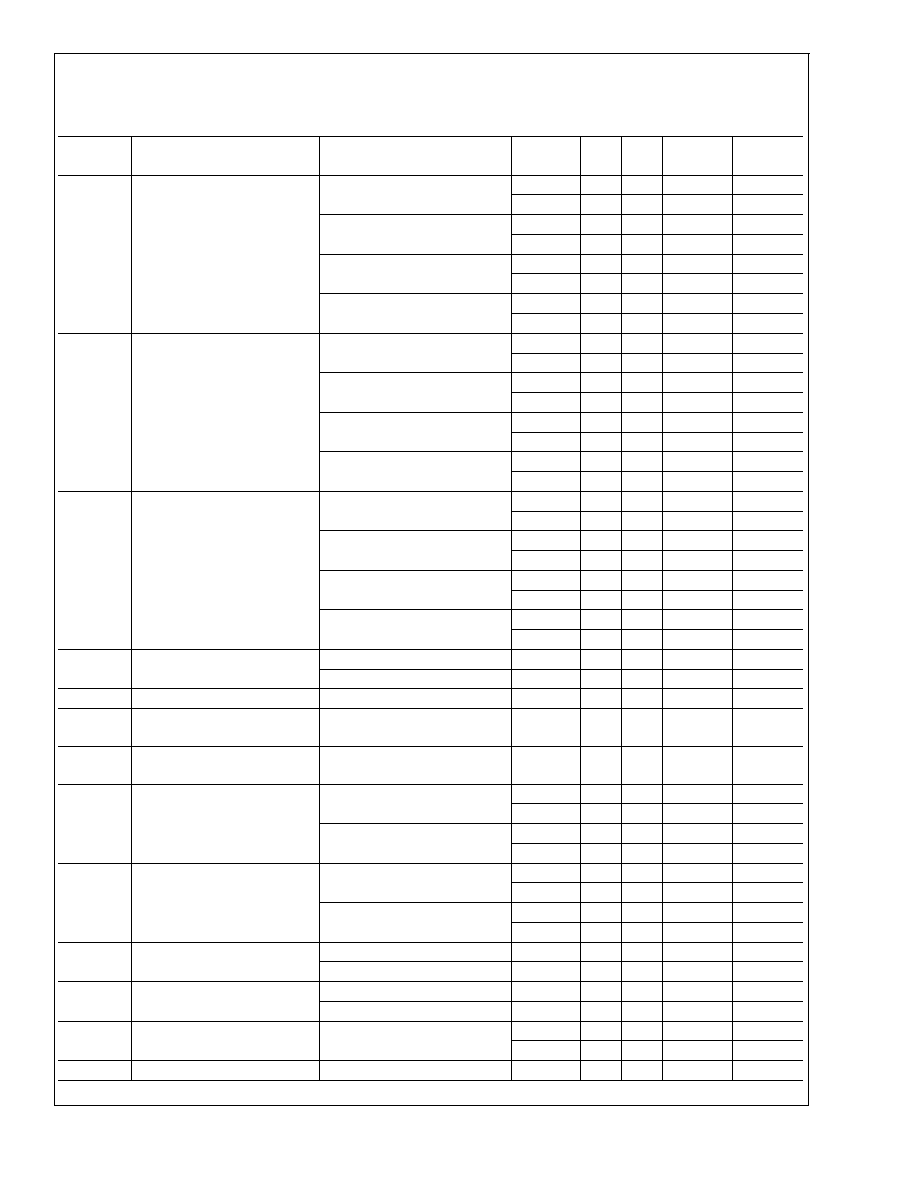
JAN Electrical Characteristics
DC Parameters
The following conditions apply, unless otherwise specified.
-V
CC
= 0V
Symbol
Parameters
Conditions
Notes
Min
Max
Unit
Sub-
groups
V
IO
Input Offset Voltage
+V
CC
= 30V, V
O
= 15V
-5.0
5.0
mV
1
-7.0
7.0
mV
2, 3
+V
CC
= 2V, -V
CC
= -28V,
V
O
= -13V
-5.0
5.0
mV
1
-7.0
7.0
mV
2, 3
+V
CC
= 5V, V
O
= 1.4V
-5.0
5.0
mV
1
-7.0
7.0
mV
2, 3
+V
CC
= 2V, -V
CC
= -3V,
V
O
= -1.6V
-5.0
5.0
mV
1
-7.0
7.0
mV
2, 3
I
IO
Input Offset Current
+V
CC
= 30V, R
S
= 20K
,
V
O
= 15V
(Note 8)
-25
25
nA
1, 2
(Note 8)
-75
75
nA
3
+V
CC
= 2V, -V
CC
= -28V,
R
S
= 20K
, V
O
= -13V
(Note 8)
-25
25
nA
1, 2
(Note 8)
-75
75
nA
3
+V
CC
= 5V, R
S
= 20K
,
V
O
= 1.4V
(Note 8)
-25
25
nA
1, 2
(Note 8)
-75
75
nA
3
+V
CC
= 2V, -V
CC
= -3V,
R
S
= 20K
, V
O
= -1.6V
(Note 8)
-25
25
nA
1, 2
(Note 8)
-75
75
nA
3
+/-I
IB
Input Bias Current
+V
CC
= 30V, R
S
= 20K
,
V
O
= 15V
(Note 8)
-100
+0.1
nA
1, 2
(Note 8)
-200
+0.1
nA
3
+V
CC
= 2V, -V
CC
= -28V,
R
S
= 20K
, V
O
= -13V
(Note 8)
-100
+0.1
nA
1, 2
(Note 8)
-200
+0.1
nA
3
+V
CC
= 5V, R
S
= 20K
,
V
O
= 1.4V
(Note 8)
-100
+0.1
nA
1, 2
(Note 8)
-200
+0.1
nA
3
+V
CC
= 2V, -V
CC
= -3V,
R
S
= 20K
, V
O
= -1.6V
(Note 8)
-100
+0.1
nA
1, 2
(Note 8)
-200
+0.1
nA
3
CMRR
Input Voltage Common Mode
Rejection
+V
CC
= 30V
76
dB
1, 2, 3
+V
CC
= 5V
70
dB
1, 2, 3
I
CEX
Output Leakage
+V
CC
= 30V, V
O
= +30V
1.0
µA
1, 2, 3
+I
IL
Input Leakage Current
+V
CC
= 36V, V + i = 34V,
V - i = 0V
-500
500
nA
1, 2, 3
-I
IL
Input Leakage Current
+V
CC
= 36V, V + i = 0V,
V - i = 34V
-500
500
nA
1, 2, 3
V
OL
Logical "0" Output Voltage
+V
CC
= 4.5V, I
O
= 4mA
0.4
V
1
0.7
V
2, 3
+V
CC
= 4.5V, I
O
= 8mA
1.5
V
1
2.0
V
2, 3
I
CC
Power Supply Current
+V
CC
= 5V, V
ID
= 15mV
2.0
mA
1, 2
3.0
mA
3
+V
CC
= 30V, V
ID
= 15mV
3.0
mA
1, 2
4.0
mA
3
Delta V
IO
/
Delta T
Temperature Coefficient of
Input Offset Voltage
25°C
T
A
125°C
(Note 9)
-25
25
µV/°C
2
-55°C
T
A
25°C
(Note 9)
-25
25
µV/°C
3
Delta I
IO
/
Delta T
Temperature Coefficient of
Input Offset Current
25°C
T
A
125°C
(Note 9)
-300
300
pA/°C
2
-55°C
T
A
25°C
(Note 9)
-400
400
pA/°C
3
A
VS
Open Loop Voltage Gain
+V
CC
=15V, R
L
=15K
,
1V
V
O
11V
(Note 10)
50
V/mV
4
(Note 10)
25
V/mV
5, 6
V
IO
Tempco Screen
4.0
mV
LM139JAN
www.national.com
5