TL F 6393
54LS153DM54LS153DM74LS153
Dual
4-Line
to
1-Line
Data
SelectorsMultiplexers
June 1989
54LS153 DM54LS153 DM74LS153
Dual 4-Line to 1-Line Data Selectors Multiplexers
General Description
Each of these data selectors multiplexers contains invert-
ers and drivers to supply fully complementary on-chip bina-
ry decoding data selection to the AND-OR-invert gates
Separate strobe inputs are provided for each of the two
four-line sections
Features
Y
Permits multiplexing from N lines to 1 line
Y
Performs at parallel-to-serial conversion
Y
Strobe (enable) line provided for cascading (N lines to
n lines)
Y
High fan-out low impedance totem pole outputs
Y
Typical average propagation delay times
From data 14 ns
From strobe 19 ns
From select 22 ns
Y
Typical power dissipation 31 mW
Y
Alternate Military Aerospace device (54LS153) is avail-
able Contact a National Semiconductor Sales Office
Distributor for specifications
Connection Diagram
Dual-In-Line Package
TL F 6393 � 1
Order Number 54LS153DMQB 54LS153FMQB
54LS153LMQB DM54LS153J DM54LS153W
DM74LS153M or DM74LS153N
See NS Package Number E20A J16A M16A
N16E or W16A
Logic Diagram
TL F 6393 � 2
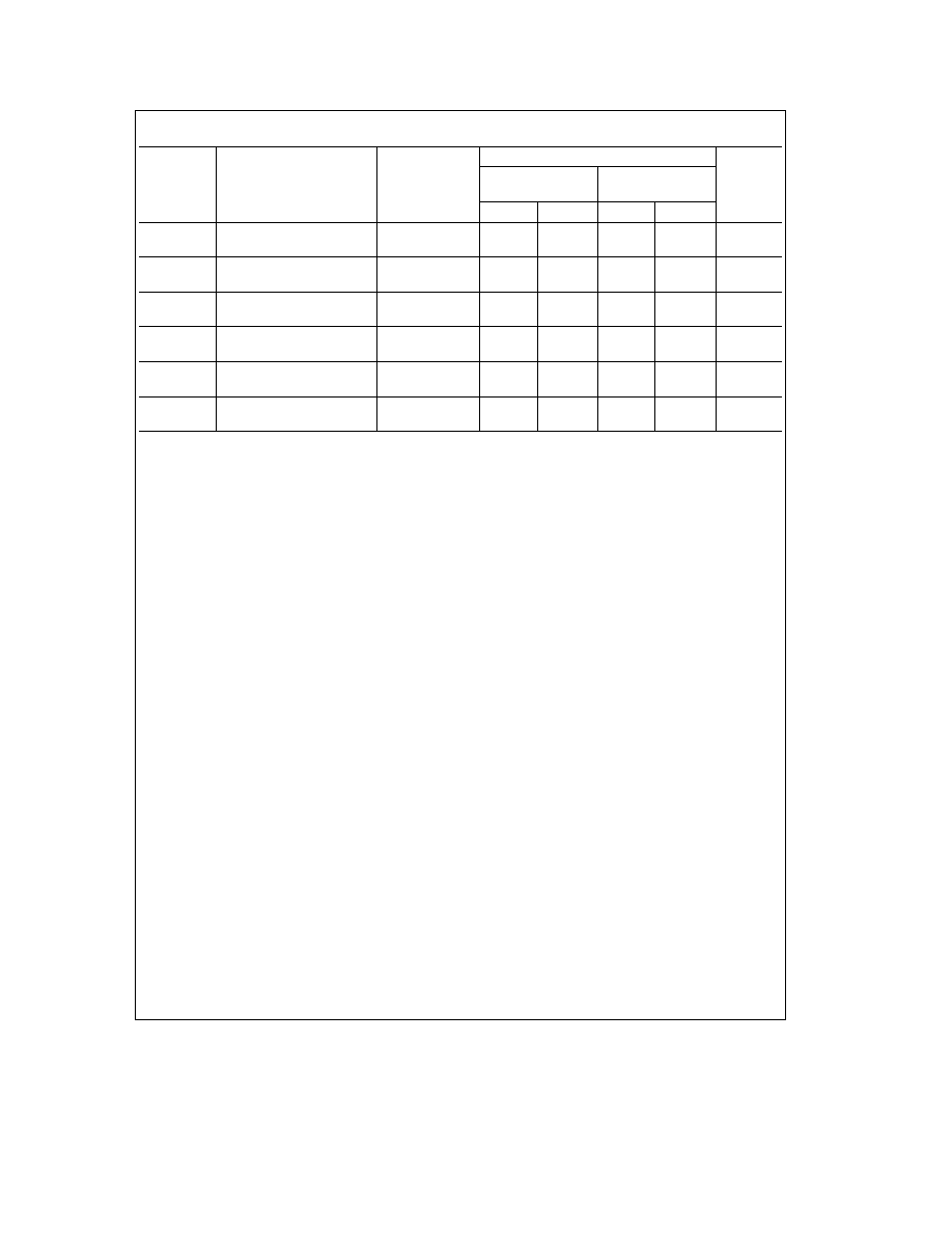
Function Table
Select
Data Inputs
Strobe
Output
Inputs
B
A
C0
C1
C2
C3
G
Y
X
X
X
X
X
X
H
L
L
L
L
X
X
X
L
L
L
L
H
X
X
X
L
H
L
H
X
L
X
X
L
L
L
H
X
H
X
X
L
H
H
L
X
X
L
X
L
L
H
L
X
X
H
X
L
H
H
H
X
X
X
L
L
L
H
H
X
X
X
H
L
H
Select inputs A and B are common to both sections
H
e
High Level L
e
Low Level X
e
Don't Care
C1995 National Semiconductor Corporation
RRD-B30M105 Printed in U S A
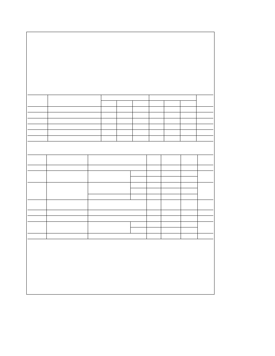
Absolute Maximum Ratings
(Note)
If Military Aerospace specified devices are required
please contact the National Semiconductor Sales
Office Distributors for availability and specifications
Supply Voltage
7V
Input Voltage
7V
Operating Free Air Temperature Range
DM54LS and 54LS
b
55 C to
a
125 C
DM74LS
0 C to
a
70 C
Storage Temperature Range
b
65 C to
a
150 C
Note
The ``Absolute Maximum Ratings'' are those values
beyond which the safety of the device cannot be guaran-
teed The device should not be operated at these limits The
parametric values defined in the ``Electrical Characteristics''
table are not guaranteed at the absolute maximum ratings
The ``Recommended Operating Conditions'' table will define
the conditions for actual device operation
Recommended Operating Conditions
Symbol
Parameter
DM54LS153
DM74LS153
Units
Min
Nom
Max
Min
Nom
Max
V
CC
Supply Voltage
4 5
5
5 5
4 75
5
5 25
V
V
IH
High Level Input Voltage
2
2
V
V
IL
Low Level Input Voltage
0 7
0 8
V
I
OH
High Level Output Current
b
0 4
b
0 4
mA
I
OL
Low Level Output Current
4
8
mA
T
A
Free Air Operating Temperature
b
55
125
0
70
C
Electrical Characteristics
over recommended operating free air temperature range (unless otherwise noted)
Symbol
Parameter
Conditions
Min
Typ
Max
Units
(Note 1)
V
I
Input Clamp Voltage
V
CC
e
Min I
I
e b
18 mA
b
1 5
V
V
OH
High Level Output
V
CC
e
Min I
OH
e
Max
DM54
2 5
3 4
V
Voltage
V
IL
e
Max V
IH
e
Min
DM74
2 7
3 4
V
OL
Low Level Output
V
CC
e
Min I
OL
e
Max
DM54
0 25
0 4
Voltage
V
IL
e
Max V
IH
e
Min
DM74
0 35
0 5
V
I
OL
e
4 mA V
CC
e
Min
DM74
0 25
0 4
I
I
Input Current
Max
V
CC
e
Max V
I
e
7V
0 1
mA
Input Voltage
I
IH
High Level Input Current
V
CC
e
Max V
I
e
2 7V
20
m
A
I
IL
Low Level Input Current
V
CC
e
Max V
I
e
0 4V
b
0 36
mA
I
OS
Short Circuit
V
CC
e
Max
DM54
b
20
b
100
mA
Output Current
(Note 2)
DM74
b
20
b
100
I
CC
Supply Current
V
CC
e
Max (Note 3)
6 2
10
mA
Note 1
All typicals are at V
CC
e
5V T
A
e
25 C
Note 2
Not more than one output should be shorted at a time and the duration should not exceed one second
Note 3
I
CC
is measured with all outputs open and all other inputs grounded
2
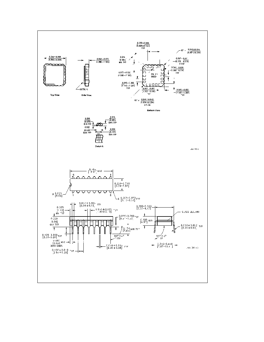
Physical Dimensions
inches (millimeters)
Ceramic Leadless Chip Carrier Package (E)
Order Number 54LS153LMQB
NS Package Number E20A
16-Lead Ceramic Dual-In-Line Package (J)
Order Number 54LS153DMQB or DM54LS153J
NS Package Number J16A
4
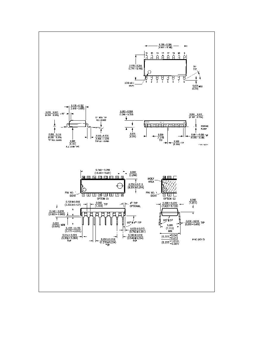
Physical Dimensions
inches (millimeters) (Continued)
16-Lead Small Outline Molded Package (M)
Order Number DM74LS153M
NS Package Number M16A
16-Lead Molded Dual-In-Line Package (N)
Order Number DM74LS153N
NS Package Number N16E
5