TL F 6396
54LS157DM54LS157DM74LS157
54LS158DM54LS158DM74LS158
Quad
2-Line
to
1-Line
Data
SelectorsMultiplexers
June 1989
54LS157 DM54LS157 DM74LS157
54LS158 DM54LS158 DM74LS158
Quad 2-Line to 1-Line Data Selectors Multiplexers
General Description
These data selectors multiplexers contain inverters and
drivers to supply full on-chip data selection to the four out-
put gates A separate strobe input is provided A 4-bit word
is selected from one of two sources and is routed to the four
outputs The LS157 presents true data whereas the LS158
presents inverted data to minimize propagation delay time
Applications
Y
Expand any data input point
Y
Multiplex dual data buses
Y
Generate four functions of two variables (one variable
is common)
Y
Source programmable counters
Features
Y
Buffered inputs and outputs
Y
Typical Propagation Time
LS157
9 ns
LS158
7 ns
Y
Typical Power Dissipation
LS157
49 mW
LS158
24 mW
Y
Alternate
Military Aerospace
device
(54LS157
54LS158) is available Contact a National Semiconduc-
tor Sales Office Distributor for specifications
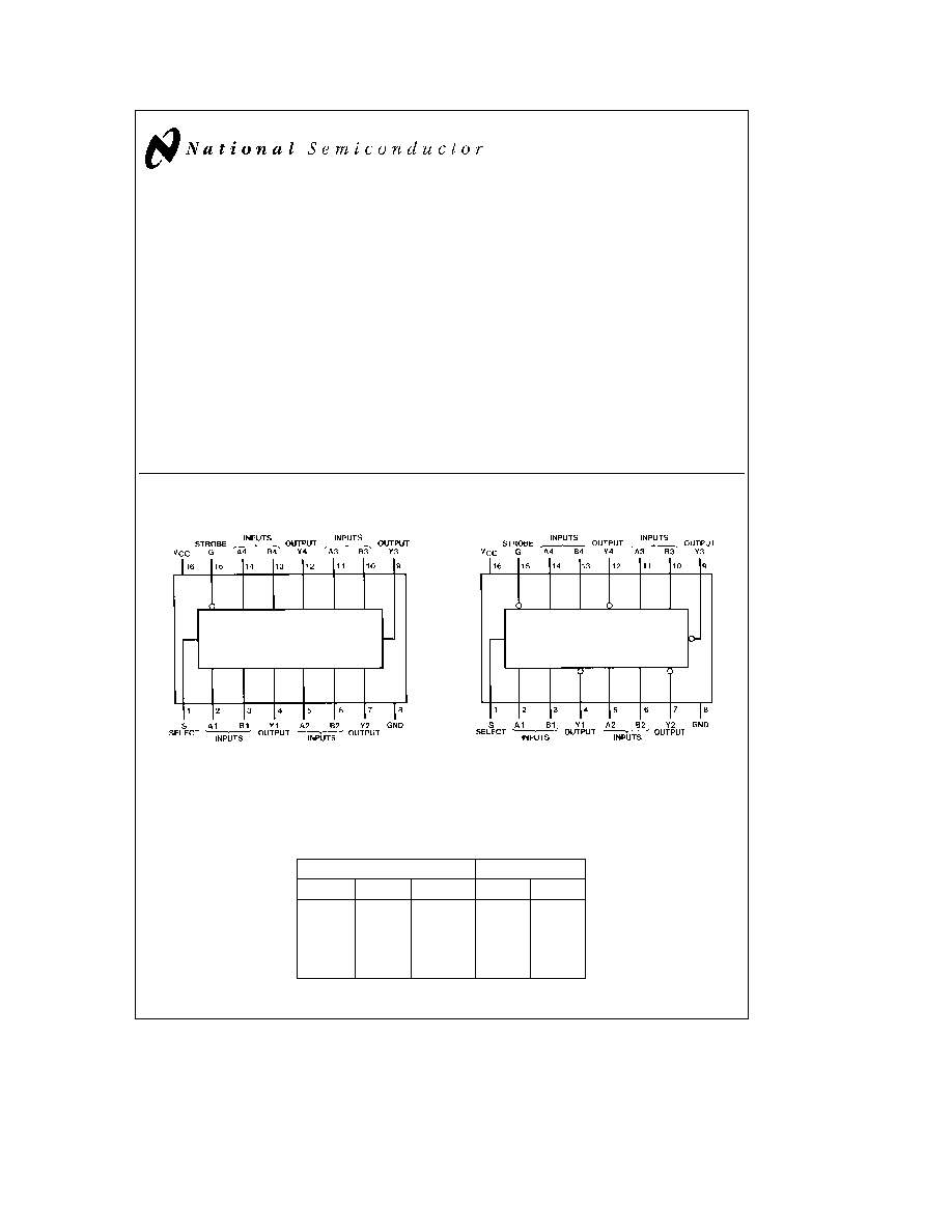
Connection Diagrams
Dual-In-Line Package
TL F 6396 ≠ 1
Order Number 54LS157DMQB 54LS157FMQB
54LS157LMQB DM54LS157J DM54LS157W
DM74LS157M or DM74LS157N
See NS Package Number E20A J16A
M16A N16E or W16A
Dual-In-Line Package
TL F 6396 ≠ 2
Order Number 54LS158DMQB 54LS158FMQB
54LS158LMQB DM54LS158J DM54LS158W
DM74LS158M or DM74LS158N
See NS Package Number E20A J16A
M16A N16E or W16A
Function Table
Inputs
Output Y
Strobe
Select
A
B
LS157
LS158
H
X
X
X
L
H
L
L
L
X
L
H
L
L
H
X
H
L
L
H
X
L
L
H
L
H
X
H
H
L
H
e
High Level L
e
Low Level X
e
Don't Care
C1995 National Semiconductor Corporation
RRD-B30M105 Printed in U S A

Absolute Maximum Ratings
(Note)
If Military Aerospace specified devices are required
please contact the National Semiconductor Sales
Office Distributors for availability and specifications
Supply Voltage
7V
Input Voltage
7V
Operating Free Air Temperature Range
DM54LS and 54LS
b
55 C to
a
125 C
DM74LS
0 C to
a
70 C
Storage Temperature Range
b
65 C to
a
150 C
Note
The ``Absolute Maximum Ratings'' are those values
beyond which the safety of the device cannot be guaran-
teed The device should not be operated at these limits The
parametric values defined in the ``Electrical Characteristics''
table are not guaranteed at the absolute maximum ratings
The ``Recommended Operating Conditions'' table will define
the conditions for actual device operation
Recommended Operating Conditions
Symbol
Parameter
DM54LS157
DM74LS157
Units
Min
Nom
Max
Min
Nom
Max
V
CC
Supply Voltage
4 5
5
5 5
4 75
5
5 25
V
V
IH
High Level Input Voltage
2
2
V
V
IL
Low Level Input Voltage
0 7
0 8
V
I
OH
High Level Output Current
b
0 4
b
0 4
mA
I
OL
Low Level Output Current
4
8
mA
T
A
Free Air Operating Temperature
b
55
125
0
70
C
'LS157 Electrical Characteristics
over recommended operating free air temperature range (unless otherwise noted)
Symbol
Parameter
Conditions
Min
Typ
Max
Units
(Note 1)
V
I
Input Clamp Voltage
V
CC
e
Min I
I
e b
18 mA
b
1 5
V
V
OH
High Level Output
V
CC
e
Min I
OH
e
Max
DM54
2 5
3 4
V
Voltage
V
IL
e
Max V
IH
e
Min
DM74
2 7
3 4
V
OL
Low Level Output
V
CC
e
Min I
OL
e
Max
DM54
0 25
0 4
Voltage
V
IL
e
Max V
IH
e
Min
DM74
0 35
0 5
V
I
OL
e
4 mA V
CC
e
Min
DM74
0 25
0 4
I
I
Input Current
Max
V
CC
e
Max
S or G
0 2
mA
Input Voltage
V
I
e
7V
A or B
0 1
I
IH
High Level Input
V
CC
e
Max
S or G
40
m
A
Current
V
I
e
2 7V
A or B
20
I
IL
Low Level Input
V
CC
e
Max
S or G
b
0 8
mA
Current
V
I
e
0 4V
A or B
b
0 4
I
OS
Short Circuit
V
CC
e
Max
DM54
b
20
b
100
mA
Output Current
(Note 2)
DM74
b
20
b
100
I
CC
Supply Current
V
CC
e
Max (Note 3)
9 7
16
mA
Note 1
All typicals are at V
CC
e
5V T
A
e
25 C
Note 2
Not more than one output should be shorted at a time and the duration should not exceed one second
Note 3
I
CC
is measured with 4 5V applied to all inputs and all outputs open
2
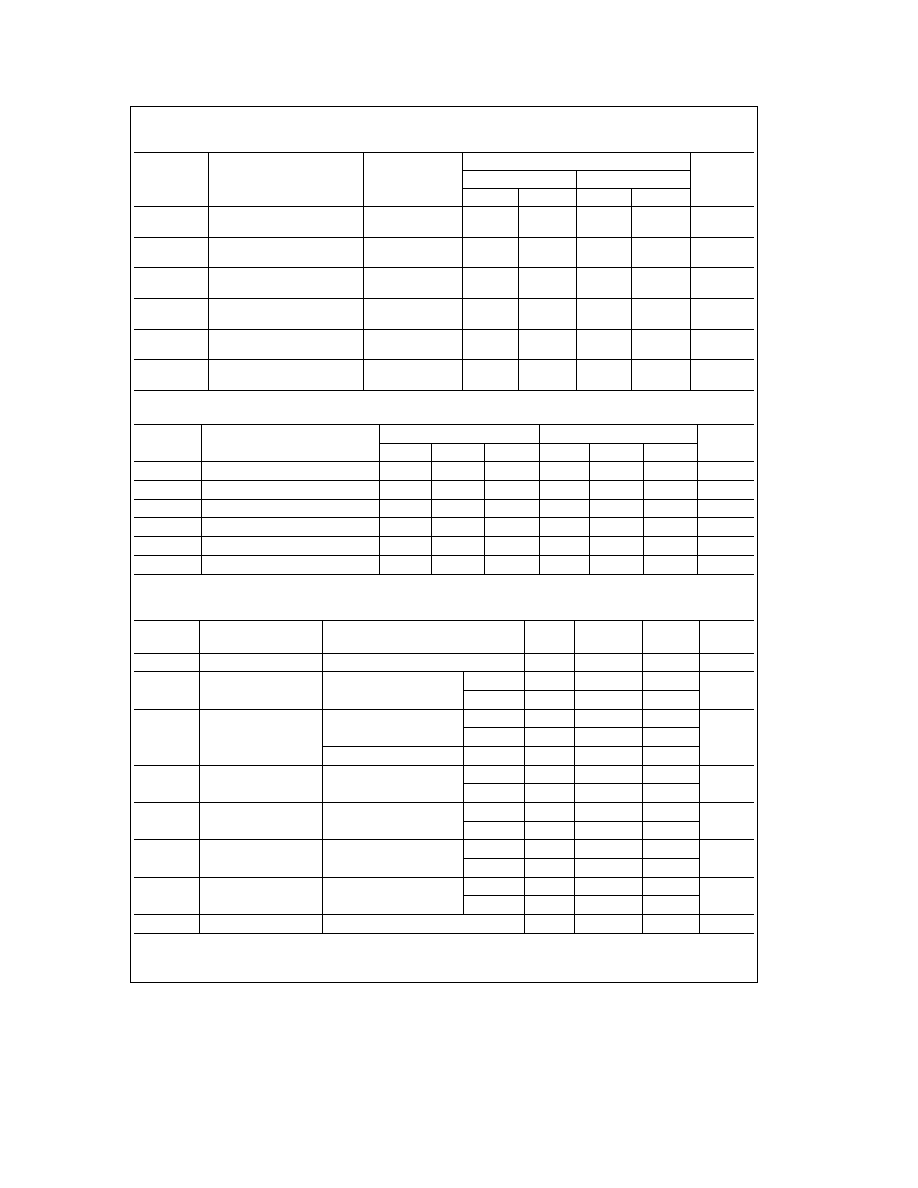
'LS157 Switching Characteristics
at V
CC
e
5V and T
A
e
25 C (See Section 1 for Test Waveforms and Output Load)
From (Input)
R
L
e
2 kX
Symbol
Parameter
To (Output)
C
L
e
15 pF
C
L
e
50 pF
Units
Min
Max
Min
Max
t
PLH
Propagation Delay Time
Data
14
18
ns
Low to High Level Output
to Y
t
PHL
Propagation Delay Time
Data
14
23
ns
High to Low Level Output
to Y
t
PLH
Propagation Delay Time
Strobe
20
24
ns
Low to High Level Output
to Y
t
PHL
Propagation Delay Time
Strobe
21
30
ns
High to Low Level Output
to Y
t
PLH
Propagation Delay Time
Select
23
28
ns
Low to High Level Output
to Y
t
PHL
Propagation Delay Time
Select
27
32
ns
High to Low Level Output
to Y
Recommended Operating Conditions
Symbol
Parameter
DM54LS158
DM74LS158
Units
Min
Nom
Max
Min
Nom
Max
V
CC
Supply Voltage
4 5
5
5 5
4 75
5
5 25
V
V
IH
High Level Input Voltage
2
2
V
V
IL
Low Level Input Voltage
0 7
0 8
V
I
OH
High Level Output Current
b
0 4
b
0 4
mA
I
OL
Low Level Output Current
4
8
mA
T
A
Free Air Operating Temperature
b
55
125
0
70
C
'LS158 Electrical Characteristics
over recommended operating free air temperature range (unless otherwise noted)
Symbol
Parameter
Conditions
Min
Typ
Max
Units
(Note 1)
V
I
Input Clamp Voltage
V
CC
e
Min I
I
e b
18 mA
b
1 5
V
V
OH
High Level Output
V
CC
e
Min I
OH
e
Max
DM54
2 5
3 4
V
Voltage
V
IL
e
Max V
IH
e
Min
DM74
2 7
3 4
V
OL
Low Level Output
V
CC
e
Min I
OL
e
Max
DM54
0 25
0 4
Voltage
V
IL
e
Max V
IH
e
Min
DM74
0 35
0 5
V
I
OL
e
4 mA V
CC
e
Min
DM74
0 25
0 4
I
I
Input Current
Max
V
CC
e
Max
S or G
0 2
mA
Input Voltage
V
I
e
7V
A or B
0 1
I
IH
High Level Input
V
CC
e
Max
S or G
40
m
A
Current
V
I
e
2 7V
A or B
20
I
IL
Low Level Input
V
CC
e
Max
S or G
b
0 8
mA
Current
V
I
e
0 4V
A or B
b
0 4
I
OS
Short Circuit
V
CC
e
Max
DM54
b
20
b
100
mA
Output Current
(Note 2)
DM74
b
20
b
100
I
CC
Supply Current
V
CC
e
Max (Note 3)
4 8
8
mA
Note 1
All typicals are at V
CC
e
5V T
A
e
25 C
Note 2
Not more than one output should be shorted at a time and the duration should not exceed one second
Note 3
I
CC
is measured with 4 5V applied to all inputs and all outputs open
3