 | –≠–ª–µ–∫—Ç—Ä–æ–Ω–Ω—ã–π –∫–æ–º–ø–æ–Ω–µ–Ω—Ç: L4952TS | –°–∫–∞—á–∞—Ç—å:  PDF PDF  ZIP ZIP |
LM4952
3.1W Stereo-SE Audio Power Amplifier
with DC Volume Control
General Description
The LM4952 is a dual audio power amplifier primarily de-
signed for demanding applications in flat panel monitors and
TV's. It is capable of delivering 3.1 watts per channel to a 4
single-ended load with less than 1% THD+N when powered
by a 12V
DC
power supply.
Eliminating external feedback resistors, an internal, DC-
controlled, volume control allows easy and variable gain
adjustment.
Boomer audio power amplifiers were designed specifically to
provide high quality output power with a minimal amount of
external components. The LM4952 does not require boot-
strap capacitors or snubber circuits. Therefore, it is ideally
suited for display applications requiring high power and mini-
mal size.
The LM4952 features a low-power consumption active-low
shutdown mode. Additionally, the LM4952 features an inter-
nal thermal shutdown protection mechanism along with short
circuit protection.
The LM4952 contains advanced pop & click circuitry that
eliminates noises which would otherwise occur during
turn-on and turn-off transitions.
Key Specifications
j
Quiscent Power Supply Current
18mA (typ)
j
P
OUT
V
DD
= 12V, R
L
= 4
, 10% THD+N
3.8W (typ)
j
Shutdown current
55µA (typ)
Features
n
Pop & click circuitry eliminates noise during turn-on and
turn-off transitions
n
Low current, active-low shutdown mode
n
Low quiescent current
n
Stereo 3.8W output, R
L
= 4
n
DC-controlled volume control
n
Short circuit protection
Applications
n
Flat Panel Monitors
n
Flat panel TV's
n
Computer Sound Cards
Connection Diagram
200809E9
Top View
Order Number LM4952TS
See NS Package Number TS9A
U = Wafer Fab Code
Z = Assembly Plant Code
XY = Date Coce
TT = Die Traceability
L4952TS = LM4952TS
Boomer
Æ
is a registered trademark of National Semiconductor Corporation.
August 2004
LM4952
3.1W
Stereo-SE
Stereo
Audio
Power
Amplifier
with
DC
V
olume
Control
© 2004 National Semiconductor Corporation
DS200809
www.national.com

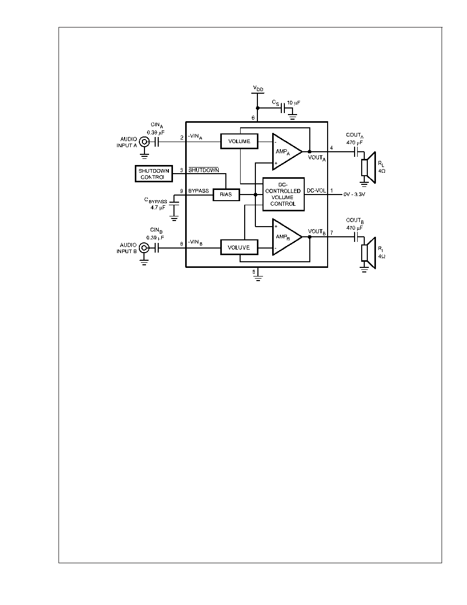
Typical Application
200809E8
FIGURE 1. Typical LM4952 SE Audio Amplifier Application Circuit
LM4952
www.national.com
2

Absolute Maximum Ratings
(Notes 1, 2)
If Military/Aerospace specified devices are required,
please contact the National Semiconductor Sales Office/
Distributors for availability and specifications.
Supply Voltage (pin 6, referenced
to GND, pins 4 and 5)
18.0V
Storage Temperature
-65∞C to +150∞C
Input Voltage
pins 4, 6, and 7
-0.3V to V
DD
+ 0.3V
pins 1, 2, 3, 8, and 9
-0.3V to 9.5V
Power Dissipation (Note 3)
Internally limited
ESD Susceptibility (Note 4)
2000V
ESD Susceptibility (Note 5)
200V
Junction Temperature
150∞C
Thermal Resistance
JC
(TS)
4∞C/W
JA
(TS) (Note 3)
20∞C/W
Operating Ratings
Temperature Range
T
MIN
T
A
T
MAX
-40∞C
T
A
85∞C
Supply Voltage
9.6V
V
DD
16V
Electrical Characteristics V
DD
= 12V
(Notes 1, 2)
The following specifications apply for V
DD
= 12V, A
V
= 20dB (nominal), R
L
= 4
, and T
A
= 25∞C unless otherwise noted.
Symbol
Parameter
Conditions
LM4952
Units
(Limits)
Typical
(Note 6)
Limit
(Notes 7, 8)
I
DD
Quiescent Power Supply Current
V
IN
= 0V, I
O
= 0A, No Load
18
35
mA (max)
I
SD
Shutdown Current
V
SHUTDOWN
= GND (Note 9)
55
85
µA (max)
R
IN
Amplifier Input Resistance
V
DC VOL
= V
DD
/2
44
k
V
DC VOL
= GND
200
k
V
IN
Amplifier Input Signal
V
DD
/2
V
p-p
(max)
V
SDIH
Shutdown Voltage Input High
2.0
V
DD
/2
V (min)
V (max)
V
SDIL
Shutdown Voltage Input Low
0.4
V (max)
T
WU
Wake-up Time
C
B
= 4.7µF
440
ms
TSD
Thermal Shutdown Temperature
170
∞C
P
O
Output Power
f = 1kHz,
THD+N = 1%
THD+N = 10%
3.1
3.8
2.8
W (min)
THD+N
Total Harmomic Distortion + Noise
P
O
= 2.0Wrms, f = 1kHz
0.08
%
e
OS
Output Noise
A-Weighted Filter, V
IN
= 0V,
Input Referred
8
µV
X
TALK
Channel Separation
f
IN
= 1kHz, P
O
= 1W,
Input Referred
R
L
= 8
R
L
= 4
78
72
dB
PSRR
Power Supply Rejection Ratio
V
RIPPLE
= 200mV
p-p
, f = 1kHz,
Input Referred
89
80
dB (min)
I
OL
Output Current Limit
V
IN
= 0V, R
L
= 500m
5
A
LM4952
www.national.com
3
Electrical Characteristics for Volume Control
(Notes 1, 2)
The following specifications apply for V
DD
= 12V, A
V
= 20dB (nominal), and T
A
= 25∞C unless otherwise noted.
Symbol
Parameter
Conditions
LM4952
Units
(Limits)
Typical
(Note 6)
Limit
(Note 7)
VOL
max
Gain
V
DC-VOL
= Full scale, No Load
20
dB
VOL
min
Gain
V
DC-VOL
= +1LSB, No Load
-46
dB
A
M
Mute Attenuation
V
DC-VOL
= 0V, No Load
75
63
dB (min)
Note 1: All voltages are measured with respect to the GND pin, unless otherwise specified.
Note 2: Absolute Maximum Ratings indicate limits beyond which damage to the device may occur. Operating Ratings indicate conditions for which the device is
functional, but do not guarantee specific performance limits. Electrical Characteristics state DC and AC electrical specifications under particular test conditions which
guarantee specific performance limits. This assumes that the device is within the Operating Ratings. Specifications are not guaranteed for parameters where no limit
is given, however, the typical value is a good indication of device performance.
Note 3: The maximum power dissipation must be derated at elevated temperatures and is dictated by T
JMAX
,
JA
, and the ambient temperature, T
A
. The maximum
allowable power dissipation is P
DMAX
= (T
JMAX
- T
A
) /
JA
or the given in Absolute Maximum Ratings, whichever is lower. For the LM4952 typical application (shown
in Figure 1) with V
DD
= 12V, R
L
= 4
stereo operation the total power dissipation is 3.65W.
JA
= 20∞C/W for the TO263 package mounted to 16in
2
heatsink surface
area.
Note 4: Human body model, 100pF discharged through a 1.5k
resistor.
Note 5: Machine Model, 220pF≠240pF discharged through all pins.
Note 6: Typicals are measured at 25∞C and represent the parametric norm.
Note 7: Limits are guaranteed to National's AOQL (Average Outgoing Quality Level).
Note 8: Datasheet min/max specification limits are guaranteed by design, test, or statistical analysis.
Note 9: Shutdown current is measured in a normal room environment. The Shutdown pin should be driven as close as possible to GND for minimum shutdown
current.
External Components Description
Refer to Figure 1
Components
Functional Description
1. C
IN
This is the input coupling capacitor. It blocks DC voltage at the amplifier's inverting input. C
IN
and R
IN
create a highpass filter. The filter's cutoff frequency is f
C
= 1/(2
R
IN
C
IN
). Refer to the SELECTING
EXTERNAL COMPONENTS, for an explanation of determining C
IN
's value.
2. C
S
The supply bypass capacitor. Refer to the POWER SUPPLY BYPASSING section for information about
properly placing, and selecting the value of, this capacitor.
3. C
BYPASS
This capacitor filters the half-supply voltage present on the BYPASS pin. Refer to the Application section,
SELECTING EXTERNAL COMPONENTS, for information about properly placing, and selecting the value
of, this capacitor.
LM4952
www.national.com
4

Typical Performance Characteristics
A
V
= 20dB and T
A
= 25∞C, unless otherwise noted.
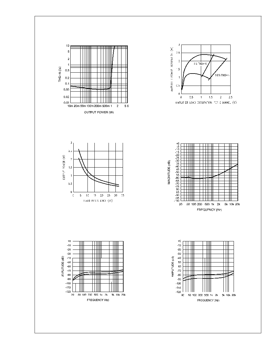
THD+N vs Frequency
THD+N vs Frequency
200809F8
V
DD
= 12V, R
L
= 4
,
P
OUT
= 2W, C
IN
= 1.0µF
200809F9
V
DD
= 12V, R
L
= 8
,
P
OUT
= 1W, C
IN
= 1.0µF
THD+N vs Output Power
THD+N vs Output Power
200809G0
V
DD
= 12V, R
L
= 4
,
f
IN
= 1kHz
200809G1
V
DD
= 12V, R
L
= 8
,
f
IN
= 1kHz
LM4952
www.national.com
5
Typical Performance Characteristics
A
V
= 20dB and T
A
= 25∞C, unless otherwise noted.
(Continued)
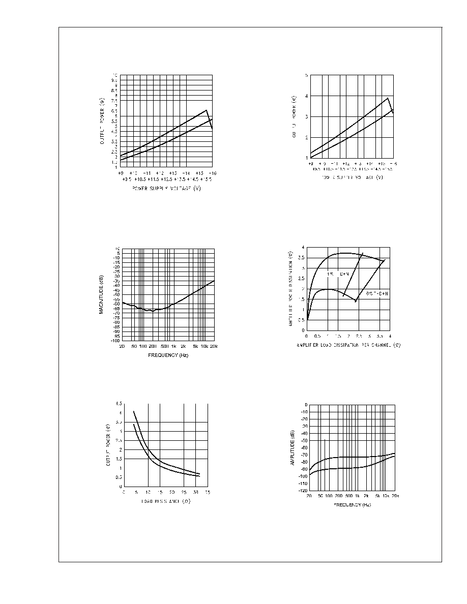
Output Power vs Power Supply Voltage
Output Power vs Power Supply Voltage
20080909
R
L
= 4
, f
IN
= 1kHz
both channels driven and loaded (average shown),
at (from top to bottom at 12V):
THD+N = 10%, THD+N = 1%
20080910
R
L
= 8
, f
IN
= 1kHz
both channels driven and loaded (average shown),
at (from top to bottom at 12V):
THD+N = 10%, THD+N = 1%
Power Supply Rejection vs Frequency
Total Power Dissipation vs Load Dissipation
200809F7
V
DD
= 12V, R
L
= 4
,
V
RIPPLE
= 200mV
p-p
20080913
V
DD
= 12V, f
IN
= 1kHz,
at (from top to bottom at 1W):
R
L
= 4
, R
L
= 8
Output Power vs Load Resistance
Channel-to-Channel Crosstalk vs Frequency
20080914
V
DD
= 12V, f
IN
= 1kHz,
at (from top to bottom at 15
):
THD+N = 10%, THD+N = 1%
20080915
V
DD
= 12V, R
L
= 4
, P
OUT
= 1W, Input Referred
at (from top to bottom at 1kHz): V
INB
driven,
V
OUTA
measured, V
INA
driven, V
OUTB
measured
LM4952
www.national.com
6
Typical Performance Characteristics
A
V
= 20dB and T
A
= 25∞C, unless otherwise noted.
(Continued)
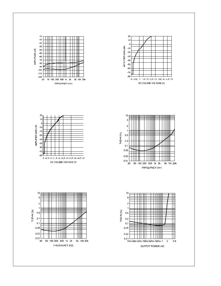
Channel-to-Channel Crosstalk vs Frequency
Amplifier Gain vs DC Volume Voltage
20080916
V
DD
= 12V, R
L
= 8
, P
OUT
= 1W, Input Referred
at (from top to bottom at 1kHz): V
INB
driven,
V
OUTA
measured, V
INA
driven, V
OUTB
measured
200809F5
V
DD
= 12V, R
L
= 8
, at (from top to bottom at 1.5V):
Decreasing DC Volume Voltage, Increasing DC Volume
Voltage
Amplifier Gain vs Part-to-Part DC Volume Voltage
Variation (Five parts)
THD+N vs Frequency
200809F6
V
DD
= 12V, R
L
= 8
,
200809G2
V
DD
= 9.6V, R
L
= 4
,
P
OUT
= 1.1W, C
IN
= 1.0µF
THD+N vs Frequency
THD+N vs Output Power
200809G3
V
DD
= 9.6V, R
L
= 8
,
P
OUT
= 850mW, C
IN
= 1.0µF
200809G4
V
DD
= 9.6V, R
L
= 4
,
f
IN
= 1kHz
LM4952
www.national.com
7
Typical Performance Characteristics
A
V
= 20dB and T
A
= 25∞C, unless otherwise noted.
(Continued)
THD+N vs Output Power
Total Power Dissipation vs Load Dissipation
200809G5
V
DD
= 9.6V, R
L
= 8
,
f
IN
= 1kHz
20080919
V
DD
= 9.6V, f
IN
= 1kHz
at (from top to bottom at 1W):
R
L
= 4
, R
L
= 8
Output Power vs Load Resistance
Power Supply Rejection vs Frequency
20080920
V
DD
= 9.6V, f
IN
= 1kHz,
at (from top to bottom at 15
):
THD+N = 10%, THD+N = 1%
200809G6
V
DD
= 9.6V, R
L
= 4
,
V
RIPPLE
= 200mV
P-P
Channel-to Channel Crosstalk vs Frequency
Channel-to Channel Crosstalk vs Frequency
20080921
V
DD
= 9.6V, R
L
= 4
, P
OUT
= 1W, Input Referred
at (from top to bottom at 1kHz): V
INB
driven, V
OUTA
measured; V
INA
driven, V
OUTB
measured
20080922
V
DD
= 9.6V, R
L
= 8
, P
OUT
= 1W, Input Referred
at (from top to bottom at 1kHz): V
INB
driven, V
OUTA
measured; V
INA
driven, V
OUTB
measured
LM4952
www.national.com
8
Typical Performance Characteristics
A
V
= 20dB and T
A
= 25∞C, unless otherwise noted.
(Continued)
THD+N vs Frequency
THD+N vs Frequency
200809G7
V
DD
= 14V, R
L
= 4
,
P
OUT
= 2W, C
IN
= 1.0µF
200809G8
V
DD
= 14V, R
L
= 8
,
P
OUT
= 1W, C
IN
= 1.0µF
THD+N vs Output Power
THD+N vs Output Power
200809G9
V
DD
= 14V, R
L
= 4
,
f
IN
= 1kHz
200809H0
V
DD
= 14V, R
L
= 8
f
IN
= 1kHz
Power Supply Rejection vs Frequency
Output Power vs Load Resistance
200809H1
V
DD
= 14V, R
L
= 4
V
RIPPLE
= 200mV
P-P
20080925
V
DD
= 15V, f
IN
= 1kHz,
at (from top to bottom at 2W):
R
L
= 4
, R
L
= 8
LM4952
www.national.com
9
Typical Performance Characteristics
A
V
= 20dB and T
A
= 25∞C, unless otherwise noted.
(Continued)
THD+N vs Output Power
THD+N vs Output Power
20080926
V
DD
= 15V, at (from top to bottom at 15
):
THD+N = 10%, THD+N = 1%, f
IN
= 1kHz
20080927
V
DD
= 16V, R
L
= 4
,
f
IN
= 1kHz
Channel-to-Channel Crosstalk vs Frequency
Channel-to-Channel Crosstalk vs Frequency
20080928
V
DD
= 16V, R
L
= 4
, P
OUT
= 1W, Input Referred
at (from top to bottom at 1kHz): V
INB
driven, V
OUTA
measured; V
INA
driven, V
OUTB
measured
20080929
V
DD
= 16V, R
L
= 8
, P
OUT
= 1W, Input Referred
at (from top to bottom at 1kHz): V
INB
driven, V
OUTA
measured; V
INA
driven, V
OUTB
measured
Power Supply Current vs Power Supply Voltage
Clipping Voltage vs Power Supply Voltage
200809H2
R
L
= 4
,
V
IN
= 0V, R
SOURCE
= 50
20080931
R
L
= 4
, f
IN
= 1kHz
at (from top to bottom at 12.5V):
positive signal swing, negative signal swing
LM4952
www.national.com
10
Typical Performance Characteristics
A
V
= 20dB and T
A
= 25∞C, unless otherwise noted.
(Continued)
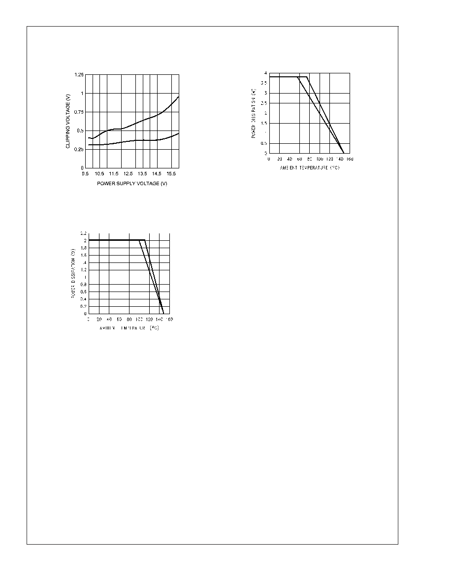
Clipping Voltage vs Power Supply Voltage
Power Dissipation vs Ambient Temperature
20080932
R
L
= 8
, f
IN
= 1kHz
at (from to bottom at 12.5V):
positive signal swing, negative signal swing
20080933
V
DD
= 12V, R
L
= 4
(SE), f
IN
= 1kHz,
(from to bottom at 80∞C): 16in
2
copper plane heatsink
area, 8in
2
copper plane heatsink area
Power Dissipation vs Ambient Temperature
20080934
V
DD
= 12V, R
L
= 8
, f
IN
= 1kHz,
(from to bottom at 120∞C): 16in
2
copper plane heatsink
area, 8in
2
copper plane heatsink area
LM4952
www.national.com
11
Application Information
HIGH VOLTAGE BOOMER WITH INCREASED OUTPUT
POWER
Unlike previous 5V Boomer
Æ
amplifiers, the LM4952 is de-
signed to operate over a power supply voltages range of
9.6V to 16V. Operating on a 12V power supply, the LM4952
will deliver 3.8W into a 4
SE load with no more than 10%
THD+N.
POWER DISSIPATION
Power dissipation is a major concern when designing a
successful single-ended or bridged amplifier. Equation (2)
states the maximum power dissipation point for a single-
ended amplifier operating at a given supply voltage and
driving a specified output load.
P
DMAX-SE
= (V
DD
)
2
/ (2
2
R
L
):
Single Ended
(1)
The LM4952's dissipation is twice the value given by Equa-
tion (2) when driving two SE loads. For a 12V supply and two
4
SE loads, the LM4952's dissipation is 1.82W.
The maximum power dissipation point given by Equation (1)
must not exceed the power dissipation given by Equation
(2):
P
DMAX
' = (T
JMAX
- T
A
) /
JA
(2)
The LM4952's T
JMAX
= 150∞C. In the TS package, the
LM4952's
JA
is 20∞C/W when the metal tab is soldered to a
copper plane of at least 16in
2
. This plane can be split be-
tween the top and bottom layers of a two-sided PCB. Con-
nect the two layers together under the tab with a 5x5 array of
vias. At any given ambient temperature T
A
, use Equation (2)
to find the maximum internal power dissipation supported by
the IC packaging. Rearranging Equation (2) and substituting
P
DMAX
for P
DMAX
' results in Equation (3). This equation gives
the maximum ambient temperature that still allows maximum
stereo power dissipation without violating the LM4952's
maximum junction temperature.
T
A
= T
JMAX
- P
DMAX-SE
JA
(3)
For a typical application with a 12V power supply and an SE
4
load, the maximum ambient temperature that allows
maximum stereo power dissipation without exceeding the
maximum junction temperature is approximately 77∞C for the
TS package.
T
JMAX
= P
DMAX-MONOBTL
JA
+ T
A
(4)
Equation (4) gives the maximum junction temperature
T
JMAX
. If the result violates the LM4952's 150∞C, reduce the
maximum junction temperature by reducing the power sup-
ply voltage or increasing the load resistance. Further allow-
ance should be made for increased ambient temperatures.
The above examples assume that a device is operating
around the maximum power dissipation point. Since internal
200809E8
FIGURE 2. Typical LM4952 SE Application Circuit
LM4952
www.national.com
12
Application Information
(Continued)
power dissipation is a function of output power, higher am-
bient temperatures are allowed as output power or duty
cycle decreases.
If the result of Equation (1) is greater than that of Equation
(2), then decrease the supply voltage, increase the load
impedance, or reduce the ambient temperature. Further,
ensure that speakers rated at a nominal 4
do not fall below
3
. If these measures are insufficient, a heat sink can be
added to reduce
JA
. The heat sink can be created using
additional copper area around the package, with connec-
tions to the ground pins, supply pin and amplifier output pins.
Refer to the Typical Performance Characteristics curves
for power dissipation information at lower output power lev-
els.
POWER SUPPLY VOLTAGE LIMITS
Continuous proper operation is ensured by never exceeding
the voltage applied to any pin, with respect to ground, as
listed in the Absolute Maximum Ratings section.
POWER SUPPLY BYPASSING
As with any power amplifier, proper supply bypassing is
critical for low noise performance and high power supply
rejection. Applications that employ a voltage regulator typi-
cally use a 10µF in parallel with a 0.1µF filter capacitors to
stabilize the regulator's output, reduce noise on the supply
line, and improve the supply's transient response. However,
their presence does not eliminate the need for a local 10µF
tantalum bypass capacitance connected between the
LM4952's supply pins and ground. Do not substitute a ce-
ramic capacitor for the tantalum. Doing so may cause oscil-
lation. Keep the length of leads and traces that connect
capacitors between the LM4952's power supply pin and
ground as short as possible.
BYPASS PIN BYPASSING
Connecting a 4.7µF capacitor, C
BYPASS
, between the BY-
PASS pin and ground improves the internal bias voltage's
stability and improves the amplifier's PSRR. The PSRR im-
provements increase as the bypass pin capacitor value in-
creases. Too large, however, increases turn-on time. The
selection of bypass capacitor values, especially C
BYPASS
,
depends on desired PSRR requirements, click and pop per-
formance (as explained in the section, SELECTING EXTER-
NAL COMPONENTS), system cost, and size constraints.
MICRO-POWER SHUTDOWN
The LM4952 features an active-low micro-power shutdown
mode. When active, the LM4952's micro-power shutdown
feature turns off the amplifier's bias circuitry, reducing the
supply current. The low 55µA typical shutdown current is
achieved by applying a voltage to the SHUTDOWN pin that
is as near to GND as possible. A voltage that is greater than
GND may increase the shutdown current.
There are a few methods to control the micro-power shut-
down. These include using a single-pole, single-throw switch
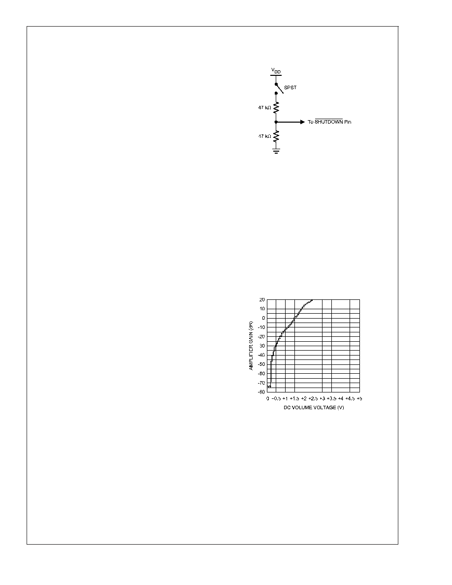
(SPST), a microprocessor, or a microcontroller. Figure 3
shows a simple switch-based circuit that can be used to
control the LM4952's shutdown fucntion. Select normal am-
plifier operation by closing the switch. Opening the switch
applies GND to the SHUTDOWN pin, activating micro-power
shutdown. The switch and resistor guarantee that the SHUT-
DOWN pin will not float. This prevents unwanted state
changes. In a system with a microprocessor or a microcon-
troller, use a digital output to apply the active-state voltage to
the SHUTDOWN pin.
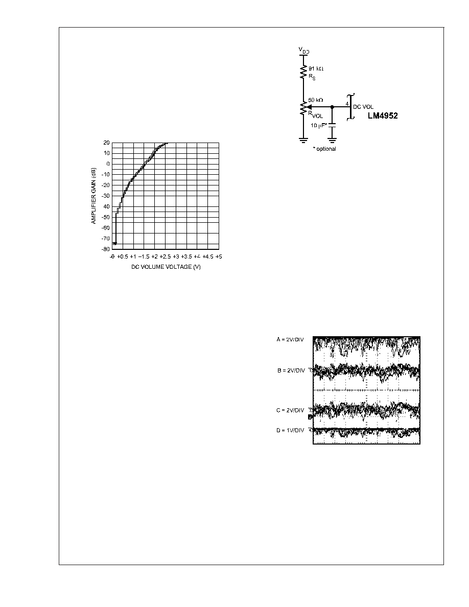
DC VOLUME CONTROL
The LM4952 has an internal stereo volume control whose
setting is a function of the DC voltage applied to the DC VOL
input pin.
The LM4952 volume control consists of 31 steps that are
individually selected by a variable DC voltage level on the
volume control pin. As shown in Figure 4, the range of the
steps, controlled by the DC voltage, is 20dB to -46dB.
The gain levels are 1dB/step from 20dB to 14dB, 2dB/step
from 14dB to -16dB, 3dB/step from -16dB to -27dB, 4dB/step
from -27db to -31dB, 5dB/step from -31dB to -46dB.
Like all volume controls, the LM4952's internal volume con-
trol is set while listening to an amplified signal that is applied
to an external speaker. The actual voltage applied to the DC
VOL input pin is a result of the volume a listener desires. As
such, the volume control is designed for use in a feedback
system that includes human ears and preferences. This
feedback system operates quite well without the need for
accurate gain. The user simply sets the volume to the de-
sired level as determined by their ear, without regard to the
actual DC voltage that produces the volume. Therefore, the
accuracy of the volume control is not critical, as long as
volume changes monotonically and step size is small
enough to reach a desired volume that is not too loud or too
200809H3
FIGURE 3. Simple switch and voltage divider
generates shutdown control signal
200809F5
FIGURE 4. Volume control response
LM4952
www.national.com
13
Application Information
(Continued)
soft. Since the gain is not critical, there may be a volume
variation from part-to-part even with the same applied DC
volume control voltage. The gain of a given LM4952 can be
set with fixed external voltage, but another LM4952 may
require a different control voltage to achieve the same gain.
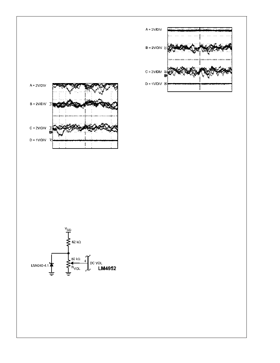
Figure 5 is a curve showing the volume variation of five
typical LM4952s as the voltage applied to the DC VOL input
pin is varied. For gains between ≠20dB and +16dB, the
typical part-to-part variation is typically
±
1dB for a given
control voltage.
VOLUME CONTROL VOLTAGE GENERATION
Figure 6 shows a simple circuit that can be used to create an
adjustable DC control voltage that is applied to the DC Vol
input. The 91k
series resistor and the 50k potentiometer
create a voltage divider between the supply voltage, V
DD
,
and GND. The series resistor's value assumes a 12V power
supply voltage. The voltage present at the node between the
series resistor and the top of the potentiometer need only be
a nominal value of 3.5V and must not exceed 9.5V, as stated
in the LM4952's Absolute Maximum Ratings.
UNREGULATED POWER SUPPLIES AND THE DC VOL
CONTROL
As an amplifier's output power increases, the current that
flows from the power supply also increases. If an unregu-
lated power supply is used, its output voltage can decrease
("droop" or "sag") as this current increases. It is not uncom-
mon for an unloaded unregulated 15V power supply con-
nected to the LM4952 to sag by as much as 2V when the
amplifier is drawing 1A to 2A while driving 4
stereo loads to
full power dissipation. Figure 7 is an oscilloscope photo
showing an unregulated power supply's voltage sag while
powering an LM4952 that is driving 4
stereo loads. The
amplifier's input is a typical music signal supplied by a CD
player. As shown, the sag can be quite significant.
This sagging supply voltage presents a potential problem
when the voltage that drives the DC Vol pin is derived from
the voltage supplied by an unregulated power supply. This is
the case for the typical volume control circuit (a 50k
poten-
tiometer in series with a 91k
resistor) shown in Figure 6.
The potentiometer's wiper is connected to the DC Vol pin.
With this circuit, power supply voltage fluctuations will be
200809F6
FIGURE 5. Typical part-to-part gain variation as a
function of DC Vol control voltage
20080966
FIGURE 6. Typical circuit used for DC voltage volume
control. Capacitor connected to DC VOL pin minimizes
voltage fluctuation when using unregulated supplies
that could cause changes in perceived volume setting
20080968
FIGURE 7. LM4952 operating on an unregulated 12V
(nominal) power supply. Wave forms shown include
V
DD
(Trace A), V
OUT A
(Trace B), V
OUT B
(Trace C), and
the DC voltage applied to the DC VOL pin (Trace D)
LM4952
www.national.com
14
Application Information
(Continued)
seen by the DC Vol input. Though attenuated by the voltage
divider action of the potentiometer and the series resistor,
these fluctuations may cause perturbations in the perceived
volume. An easy and simple solution that suppresses these
perturbations is a 10µF capacitor connected between the DC
Vol pin and ground. See the result of this capacitor in Figure
8. This capacitance can also be supplemented with bulk
capacitance in the range of 1000µF to 10,000µF connected
to the unregulated power supply's output. Figure 10 shows
how this bulk capacitance minimizes fluctuations on V
DD
.
If space constraints preclude the use of a 10µF capacitor
connected to the DC Vol pin or large amounts of bulk supply
capacitance, or if more resistance to the fluctuations is de-
sired, using an LM4040-4.1 voltage reference shown in Fig-
ure 9 is recommended. The value of the 91k
resistor,
already present in the typical volume applications circuit,
should be changed to 62k
. This sets the LM4040-4.1's bias
current at 125µA when using a nominal 12V supply, well
within the range of current needed by this reference.
SELECTING EXTERNAL COMPONENTS
Input Capacitor Value Selection
Two quantities determine the value of the input coupling
capacitor: the lowest audio frequency that requires amplifi-
cation and desired output transient suppression.
The amplifier's input resistance and the input capacitor (C
IN
)
produce a high pass filter cutoff frequency that is found using
Equation (5).
F
CIN
= 1/(2
R
IN
C
IN
)
(5)
As an example when using a speaker with a low frequency
limit of 50Hz and based on the LM4952's 44k
nominal
minimum input resistance, C
IN
, using Equation (5) is
0.072µF. The 0.39µF C
INA
shown in Figure 2 allows the
LM4952 to drive high efficiency, full range speaker whose
response extends below 30Hz.
Similarly, the output coupling capacitor and the load imped-
ance also form a high pass filter. The cutoff frequency
formed by these two components is found using Equation (6)
f
COUT
= 1/(2
R
LOAD
C
OUT
)
(6)
Expanding on the example above and assuming a nominal
speaker impedance of 4
, response below 30Hz is assured
if the output coupling capacitors have a value, using Equa-
tion (6), greater than 1330µF.
Bypass Capacitor Value
Besides minimizing the input capacitor size, careful consid-
eration should be paid to value of C
BYPASS
, the capacitor
connected to the BYPASS pin. Since C
BYPASS
determines
how fast the LM4952 settles to quiescent operation, its value
is critical when minimizing turn-on pops. The slower the
LM4952's outputs ramp to their quiescent DC voltage (nomi-
nally V
DD
/2), the smaller the turn-on pop. Choosing C
BYPASS
equal to 4.7µF along with a small value of C
IN
(in the range
of 0.1µF to 0.39µF) produces a click-less and pop-less shut-
down function. As discussed above, choosing C
IN
no larger
than necessary for the desired bandwidth helps minimize
clicks and pops.
Routing Input and BYPASS Capacitor Grounds
Optimizing the LM4952's low distortion performance is easily
accomplished by connecting the input signal's ground refer-
ence directly to the TO263's grounded tab connection. In like
20080969
FIGURE 8. Same conditions and waveforms as shown
in Figure 7, except that a 10µF capacitor has been
connected between the DC VOL pin and GND (Trace D)
20080967
FIGURE 9. Using an LM4040≠4.1 to set the maximum
DC volume control voltage and attenuate power supply
variations when using unregulated supplies that would
otherwise perturb the volume setting.
20080970
FIGURE 10. Same conditions and waveforms as shown
in Figure 8, except that a 4700µF capacitor has been
connected between the V
DD
pin and GND (Trace A)
LM4952
www.national.com
15

Application Information
(Continued)
manner, the ground lead of the capacitor connected between
the BYPASS pin and GND should also be connected to the
package's grounded tab.
OPTIMIZING CLICK AND POP REDUCTION
PERFORMANCE
The LM4952 contains circuitry that eliminates turn-on and
shutdown transients ("clicks and pops"). For this discussion,
turn-on refers to either applying the power supply voltage or
when the micro-power shutdown mode is deactivated.
As the V
DD
/4 voltage present at the BYPASS pin ramps to its
final value, the LM4952's internal amplifiers are muted. Once
the voltage at the BYPASS pin reaches V
DD
/4, the amplifiers
are unmuted.
The gain of the internal amplifiers remains unity until the
voltage on the bypass pin reaches V
DD
/4. As soon as the
voltage on the bypass pin is stable, the device becomes fully
operational and the amplifier outputs are reconnected to
their respective output pins.
In order eliminate "clicks and pops", all capacitors must be
discharged before turn-on. Rapidly switching V
DD
may not
allow the capacitors to fully discharge, which may cause
"clicks and pops".
There is a relationship between the value of C
IN
and
C
BYPASS
that ensures minimum output transient when power
is applied or the shutdown mode is deactivated. Best perfor-
mance is achieved by selecting a C
BYPASS
value that is
greater than twelve times C
IN
's value.
RECOMMENDED PRINTED CIRCUIT BOARD LAYOUT
Figure 9 through Figure 11 show the recommended two-
layer PC board layout that is optimized for the TO263-
packaged, SE-configured LM4952 and associated external
components. These circuits are designed for use with an
external 12V supply and 4
(min)(SE) speakers.
These circuit boards are easy to use. Apply 12V and ground
to the board's V
DD
and GND pads, respectively. Connect a
speaker between the board's OUT
A
and OUT
B
outputs and
respective GND pins.
LM4952
www.national.com
16
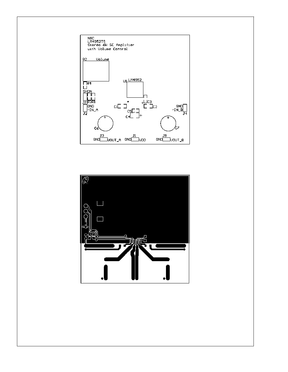
Demonstration Board Layout
200809F2
FIGURE 11. Recommended TS SE PCB Layout:
Top Silkscreen
200809F4
FIGURE 12. Recommended TS SE PCB Layout:
Top Layer
LM4952
www.national.com
17
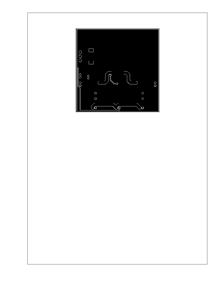
Demonstration Board Layout
(Continued)
200809F3
FIGURE 13. Recommended TS SE PCB Layout:
Bottom Layer
LM4952
www.national.com
18
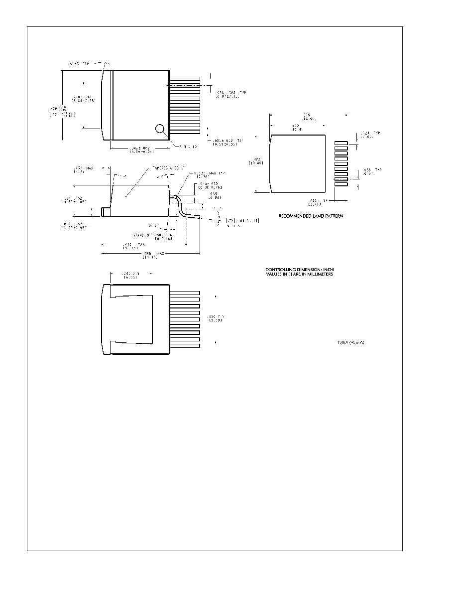
Physical Dimensions
inches (millimeters)
unless otherwise noted
Order Number LM4952TS
NS Package Number TS9A
LM4952
www.national.com
19

Notes
LIFE SUPPORT POLICY
NATIONAL'S PRODUCTS ARE NOT AUTHORIZED FOR USE AS CRITICAL COMPONENTS IN LIFE SUPPORT
DEVICES OR SYSTEMS WITHOUT THE EXPRESS WRITTEN APPROVAL OF THE PRESIDENT AND GENERAL
COUNSEL OF NATIONAL SEMICONDUCTOR CORPORATION. As used herein:
1. Life support devices or systems are devices or
systems which, (a) are intended for surgical implant
into the body, or (b) support or sustain life, and
whose failure to perform when properly used in
accordance with instructions for use provided in the
labeling, can be reasonably expected to result in a
significant injury to the user.
2. A critical component is any component of a life
support device or system whose failure to perform
can be reasonably expected to cause the failure of
the life support device or system, or to affect its
safety or effectiveness.
BANNED SUBSTANCE COMPLIANCE
National Semiconductor certifies that the products and packing materials meet the provisions of the Customer Products
Stewardship Specification (CSP-9-111C2) and the Banned Substances and Materials of Interest Specification
(CSP-9-111S2) and contain no ``Banned Substances'' as defined in CSP-9-111S2.
National Semiconductor
Americas Customer
Support Center
Email: new.feedback@nsc.com
Tel: 1-800-272-9959
National Semiconductor
Europe Customer Support Center
Fax: +49 (0) 180-530 85 86
Email: europe.support@nsc.com
Deutsch Tel: +49 (0) 69 9508 6208
English
Tel: +44 (0) 870 24 0 2171
FranÁais Tel: +33 (0) 1 41 91 8790
National Semiconductor
Asia Pacific Customer
Support Center
Email: ap.support@nsc.com
National Semiconductor
Japan Customer Support Center
Fax: 81-3-5639-7507
Email: jpn.feedback@nsc.com
Tel: 81-3-5639-7560
www.national.com
LM4952
3.1W
Stereo-SE
Stereo
Audio
Power
Amplifier
with
DC
V
olume
Control
National does not assume any responsibility for use of any circuitry described, no circuit patent licenses are implied and National reserves the right at any time without notice to change said circuitry and specifications.