
Original Creation Date: 06/20/95
Last Update Date: 09/12/02
Last Major Revision Date: 09/05/02
MNLF157-X REV 1A1
MICROCIRCUIT DATA SHEET
MONOLITHIC JFET INPUT OPERATIONAL AMPLIFIERS
General Description
These are the first monolithic JFET input operational amplifiers to incorporate well
matched, high voltage JFETs on the same chip with standard bipolar transistors (BI-FET(TM)
Technology). These amplifiers feature low input bias and offset currents/low offset
voltage and offset voltage drift, coupled with offset adjust which does not degrade drift
or common-mode rejection. The devices are also designed for high slew rate, wide
bandwidth, extremely fast settling time, low voltage and current noise and a low 1/f noise
corner.
NS Part Numbers
LF157H/883
Industry Part Number
LF157
Prime Die
LF157
Processing
MIL-STD-883, Method 5004
Quality Conformance Inspection
MIL-STD-883, Method 5005
Subgrp Description Temp ( C)
o
Static tests at
+25
2
Static tests at
+125
3
Static tests at
-55
4
Dynamic tests at
+25
5
Dynamic tests at
+125
6
Dynamic tests at
-55
7
Functional tests at
+25
8A
Functional tests at
+125
8B
Functional tests at
-55
9
Switching tests at
+25
10
Switching tests at
+125
11
Switching tests at
-55
1

MICROCIRCUIT DATA SHEET
MNLF157-X REV 1A1
Features
- Low input bias current 30 pA
- Low input offset current 3 pA
- High input impedance 10e12 Ohms
- Low input offset voltage 1 mV
- Low input offset voltage temp. drift 3 uV/ C
- Low input noise current 0.01 pA/sqrtHz
- High common-mode rejection ratio 100 dB
- Large dc voltage gain 106 dB
- Extremely fast settling time to 0.01% 1.5 uS
- Fast slew rate 50 V/uS
- Wide gain bandwidth 20 MHz
- Low input noise voltage 12 nV/sqrtHz
2

MICROCIRCUIT DATA SHEET
MNLF157-X REV 1A1
(Absolute Maximum Ratings)
(Note 1)
Supply Voltage
+22V
Differential Input Voltage
+40V
Input Voltage Range
(Note 4)
+20V
Output Short Circuit Duration
Continuous
Tjmax
150 C
Power Dissipation at Ta=25 C
560mW
(Still Air)
(Note 2, 3)
1200mW
(500 LF/Min Air Flow)
Thermal Resistance
ThetaJA
162 C/W
(Still Air)
89 C/W
(500LF/Min Air flow)
32 C/W
ThetaJC
Storage Temperature Range
-65 C < Ta < +150 C
Lead Temperature
300 C
(Soldering, 10 seconds)
ESD tolerance
(Note 5)
1200V
Note 1:
Absolute Maximum Ratings indicate limits beyond which damage to the device may occur.
Operating Ratings indicate conditions for which the device is functional, but do not
guarantee specific performance limits. For guaranteed specifications and test
conditions, see the Electrical Characteristics. Some performance characteristics may
degrade when the device is not operated under the listed test conditions.
Note 2:
The maximum power dissipation must be derated at elevated temperatures and is
dictated by Tjmax (maximum junction temperature), ThetaJA (package junction to
ambient thermal resistance), and TA (ambient temperature). The maximum allowable
power dissipation at any temperature is Pdmax = (Tjmax - TA)/ThetaJA or the number
given in the Absolute Maximum Ratings, whichever is lower.
Note 3:
Maximum Power Dissipation is deined by the package characteristics. Operating the
part near the Maximum Power Dissipation may cause the part to operate outside
guaranteed limits.
Note 4:
Unless otherwise specified the absolute maximum negative input voltage is equal to
the negative power supply voltage.
Note 5:
Human body model, 100pF discharged through 1.5k Ohms.
3
MNLF157-X REV 1A1
MICROCIRCUIT DATA SHEET
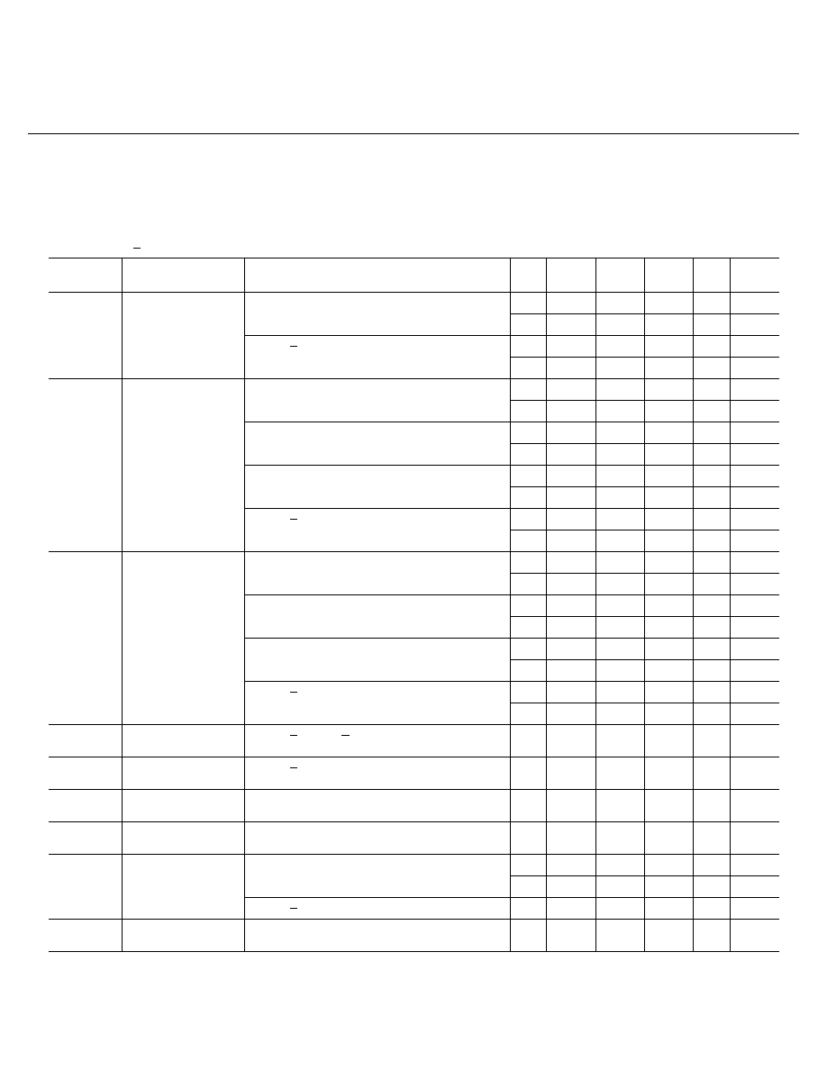
Electrical Characteristics
DC PARAMETERS
(The following conditions apply to all the following parameters, unless otherwise specified.)
DC:
Vcc = +15V, Vcm = 0V, Rs = 50 Ohms
SYMBOL
PARAMETER
CONDITIONS
NOTES
PIN-
NAME
MIN
MAX
UNIT
SUB-
GROUPS
Vio
Input Offset
Voltage
-5
5
mV
1
-7
7
mV
2, 3
Vcc = +20V
-5
5
mV
1
-7
7
mV
2, 3
Iio
Input Offset
Current
-0.02
0.02
nA
1
-20
20
nA
2, 3
Vcm = 11V
-0.02
0.02
nA
1
-20
20
nA
2, 3
Vcm = -11V
-0.02
0.02
nA
1
-20
20
nA
2, 3
Vcc = +20V
-0.02
0.02
nA
1
-20
20
nA
2, 3
Ibias
Input Bias
Current
0.1
nA
1
50
nA
2, 3
Vcm = 11V
0.1
nA
1
50
nA
2, 3
Vcm = -11V
0.1
nA
1
50
nA
2, 3
Vcc = +20V
0.1
nA
1
50
nA
2, 3
PSRR
Power Supply
Rejection Ratio
Vcc = +20V to +10V
85
dB
1, 2,
3
CMRR
Common Mode
Rejection Ratio
Vcm = +11V
85
dB
1, 2,
3
+Vio/Adj
Input Offset
Voltage Adjust
10
mV
1, 2,
3
-Vio/Adj
Input Offset
Voltage Adjust
-10
mV
1, 2,
3
Icc
Power Supply
Current
7
mA
1
9
mA
2, 3
Vcc = +20V
9
mA
1
+Ios
Short Circuit
Current
Vout = 0V
-35
-15
mA
1
4
MNLF157-X REV 1A1
MICROCIRCUIT DATA SHEET
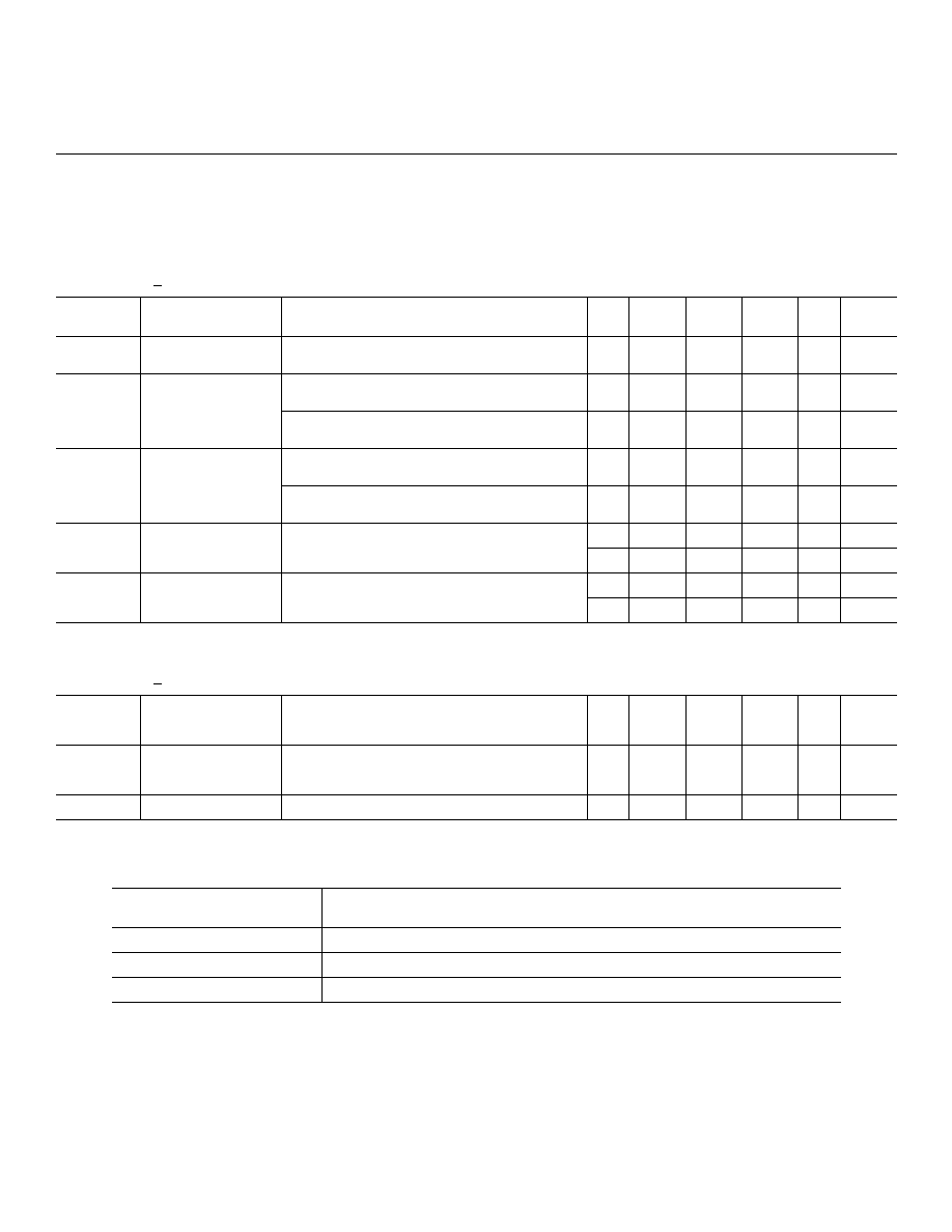
Electrical Characteristics
DC PARAMETERS(Continued)
(The following conditions apply to all the following parameters, unless otherwise specified.)
DC:
Vcc = +15V, Vcm = 0V, Rs = 50 Ohms
SYMBOL
PARAMETER
CONDITIONS
NOTES
PIN-
NAME
MIN
MAX
UNIT
SUB-
GROUPS
-Ios
Short Circuit
Current
Vout = 0V
15
35
mA
1
+Vop
Output Voltage
Swing
Rl 10K Ohms
12
V
4, 5,
6
Rl 2K Ohms
10
V
4, 5,
6
-Vop
Output Voltage
Swing
Rl 10K Ohms
-12
V
4, 5,
6
Rl 2K Ohms
-10
v
4, 5,
6
+Avs
Large Signal
Voltage Gain
Rl = 2K Ohms, Vout = 0 to 10V
50
V/mV
4
25
V/mV
5, 6
-Avs
Large Signal
Voltage Gain
Rl = 2K Ohms, Vout = 0 to -10V
50
V/mV
4
25
V/mV
5, 6
AC PARAMETERS
(The following conditions apply to all the following parameters, unless otherwise specified.)
AC:
Vcc = +15V, Vcm = 0V, Rs = 50 Ohms
+Sr
Slew Rate
Av = 5, Rload = 2K Ohms,
Cload = 100pfd, Vin = -1V to +1V,
Vout = -5V to +5V
30
V/uS
9
-Sr
Slew Rate
Av = 5, Rload = 2K Ohms,
Cload = 100pfd, Vin = +1V to -1V,
Vout = +5V to -5V
30
V/uS
9
Gbw
Gain Bandwidth
15
MHz
9
Graphics and Diagrams
GRAPHICS#
DESCRIPTION
05094HRB3
METAL CAN (H), TO-99, 8LD .200 DIA P.C. (B/I CKT)
H08CRF
METAL CAN (H), TO-99, 8LD, .200 DIA P.C. (P/P DWG)
P000295A
METAL CAN (H), 8 LEAD (PINOUT)
See attached graphics following this page.
5