 | –≠–ª–µ–∫—Ç—Ä–æ–Ω–Ω—ã–π –∫–æ–º–ø–æ–Ω–µ–Ω—Ç: LF311H | –°–∫–∞—á–∞—Ç—å:  PDF PDF  ZIP ZIP |
TL H 5703
LF111LF211LF311
Voltage
Comparators
November 1994
LF111 LF211 LF311 Voltage Comparators
General Description
The LF111 LF211 and LF311 are FET input voltage com-
parators that virtually eliminate input current errors De-
signed to operate over a 5 0V to
g
15V range the LF111
can be used in the most critical applications
The extremely low input currents of the LF111 allows the
use of a simple comparator in applications usually requiring
input current buffering Leakage testing long time delay cir-
cuits charge measurements and high source impedance
voltage comparisons are easily done
Further the LF111 can be used in place of the LM111 elimi-
nating errors due to input currents See the ``application
hints'' of the LM311 for application help
Features
Y
Eliminates input current errors
Y
Interchangeable with LM111
Y
No need for input current buffering
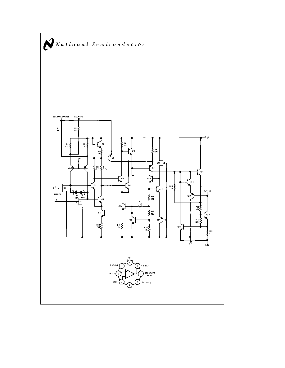
Schematic Diagram
TL H 5703 ≠ 2
Note
Do Not Ground Strobe Pin or
Balance Strobe Pin See Note 7
Connection Diagram
Metal Can Package
TL H 5703 ≠ 1
Top View
Order Number LF111H LF111H-MIL or LF311H
See NS Package Number H08C
C1995 National Semiconductor Corporation
RRD-B30M115 Printed in U S A
Absolute Maximum Ratings
If Military Aerospace specified devices are required
please contact the National Semiconductor Sales
Office Distributors for availability and specifications
(Note 8)
LF111 LF211
LF311
Total Supply Voltage (V
84
)
36V
36V
Output to Negative Supply
Voltage (V
74
)
50V
40V
Ground to Negative Supply
Voltage (V
14
)
30V
30V
Differential Input Voltage
g
30V
g
30V
Input Voltage (Note 1)
g
15V
g
15V
Power Dissipation (Note 2)
500 mW
500 mW
Output Short Circuit Duration
10 seconds
10 seconds
LF111 LF211
LF311
Operating Temp
Range
LF111
b
55 C to
a
125 C
LF211
b
25 C to
a
85 C
LF311
0 C to
a
70 C
Storage Temp
Range
b
65 C to
a
150 C
b
65 C to
a
150 C
Lead Temp
(Soldering
10 seconds)
260 C
260 C
ESD rating to be determined
Electrical Characteristics
(LF111 LF211) (Note 3)
Parameter
Conditions
Min
Typ
Max
Units
Input Offset Voltage (Note 4)
T
A
e
25 C R
S
s
50k
0 7
4 0
mV
Input Offset Current (Note 4)
T
A
e
25 C V
CM
e
0 (Note 6)
5 0
25
pA
Input Bias Current
T
A
e
25 C V
CM
e
0 (Note 6)
20
50
pA
Voltage Gain
T
A
e
25 C
40
200
V mV
Response Time (Note 5)
T
A
e
25 C
200
ns
Saturation Voltage
V
IN
s
b
5 0 mV I
OUT
e
50 mA T
A
e
25 C
0 75
1 5
V
Strobe On Current
T
A
e
25 C
3 0
mA
Output Leakage Current
V
IN
s
5 0 mV V
OUT
e
35V T
A
e
25 C
0 2
10
nA
Input Offset Voltage (Note 4)
R
S
s
50k
6 0
mV
Input Offset Current (Note 4)
V
S
e
g
15V V
CM
e
0 (Note 6)
2 0
3 0
nA
Input Bias Current
V
S
e
g
15V V
CM
e
0 (Note 6)
5 0
7 0
nA
Input Voltage Range
b
13 5
g
14
13 0
V
Saturation Voltage
V
a t
4 5V V
b
e
0
0 23
0 4
V
V
IN
s
b
6 0 mV I
OUT
s
8 0 mA
Output Leakage Current
V
IN
t
5 0 mV V
OUT
e
35V
0 1
0 5
m
A
Positive Supply Current
T
A
e
25 C
5 1
6 0
mA
Negative Supply Current
T
A
e
25 C
4 1
5 0
mA
Note 1
This rating applies for
g
15V supplies The positive input voltage limit is 30V above the negative supply The negative input voltage limit is equal to the
negative supply voltage or 30V below the positive supply whichever is less
Note 2
The maximum junction temperature of the LF111 is
a
150 C the LF211 is
a
110 C and the LF311 is
a
85 C For operating at elevated temperatures
devices in the H08 package must be derated based on a thermal resistance of
a
65 C W junction to ambient (in 400 linear feet min air flow)
a
165 C W junction
to ambient (in static air) or
a
20 C W junction to case
Note 3
These specifications apply for V
S
e g
15V and the Ground pin at ground and
b
55 C
s
T
A
s a
125 C for the LF111 unless otherwise stated With the
LF211 however all temperature specifications are limited to
b
25 C
s
T
A
s g
85 C and for the LF311 0 C
s
T
A
s a
70 C The offset voltage offset current and bias
current specifications apply for any supply voltage from a single 5 0V supply up to
g
15V supplies
Note 4
The offset voltages and offset currents given are the maximum values required to drive the output within a volt of either supply with a 1 0 mA load Thus
these parameters define an error band and take into account the worst case effects of voltage gain and input impedance
Note 5
The response time specified (see definitions) is for a 100 mV input step with 5 0 mV overdrive
Note 6
For input voltages greater than 15V above the negative supply the bias and offset currents will increase
see typical performance curves
Note 7
This specification gives the current that must be drawn from the strobe pin to ensure the output is properly disabled Do not short the strobe pin to ground
it should be current driven at 3 to 5 mA
Note 8
Refer to RETSF111X for LF111H military specifications
2

Electrical Characteristics
(LF311) (Note 3)
Parameter
Conditions
Min
Typ
Max
Units
Input Offset Voltage (Note 4)
T
A
e
25 C R
S
s
50k
2 0
10
mV
Input Offset Current (Note 4)
T
A
e
25 C V
CM
e
0 (Note 6)
5 0
75
pA
Input Bias Current
T
A
e
25 C V
CM
e
0 (Note 6)
25
150
pA
Voltage Gain
T
A
e
25 C
200
V mV
Response Time (Note 5)
T
A
e
25 C
200
ns
Saturation Voltage
V
IN
s
b
10 mV I
OUT
e
50 mA T
A
e
25 C
0 75
1 5
V
Strobe On Current
T
A
e
25 C
3 0
mA
Output Leakage Current
V
IN
t
10mV V
OUT
e
35V T
A
e
25 C
0 2
10
nA
Input Offset Voltage (Note 4)
R
S
s
50k
15
mV
Input Offset Current (Note 4)
V
S
e
g
15V V
CM
e
0 (Note 6)
1 0
nA
Input Bias Current
V
S
e
15V V
CM
e
0 (Note 6)
3 0
nA
Input Voltage Range
a
14
V
b
13 5
V
Saturation Voltage
V
a t
4 5V V
b
e
0
V
IN
s
b
10 mV I
OUT
s
8 0 mA
0 23
0 4
V
Positive Supply Current
T
A
e
25 C
5 1
7 5
mA
Negative Supply Current
T
A
e
25 C
4 1
5 0
mA
Note 1
This rating applies for
g
15V supplies The positive input voltage limit is 30V above the negative supply The negative input voltage limit is equal to the
negative supply voltage or 30V below the positive supply whichever is less
Note 2
The maximum junction temperature of the LF111 is
a
150 C the LF211 is
a
110 C and the LF311 is
a
85 C For operating at elevated temperatures
devices in the H08 package must be derated based on a thermal resistance of
a
165 C W junction to ambient or
a
20 C W junction to case
Note 3
These specifications apply for V
S
e g
15V and
b
55 C
s
T
A
s a
125 C for the LF111 unless otherwise stated With the LF211 however all temperature
specifications are limited to
b
25 C
s
T
A
s a
85 C and for the LF311 0 C
s
T
A
s a
70 C The offset voltage offset current and bias current specifications apply for
any supply voltage from a single 5 0 mV supply up to
g
15V supplies
Note 4
The offset voltages and offset currents given are the maximum values required to drive the output within a volt of either supply with a 1 0 mA load Thus
these parameters define an error band and take into account the worst case effects of voltage gain and input impedance
Note 5
The response time specified (see definitions) is for a 100 mV input step with 5 0 mV overdrive
Note 6
For input voltages greater than 15V above the negative supply the bias and offset currents will increase
see typical performance curves
Note 7
This specification gives the current that must be drawn from the strobe pin to ensure the output is properly disabled Do not short the strobe pin to ground
it should be current driven at 3 to 5 mA
Auxiliary Circuits
Offset Balancing
TL H 5703 ≠ 13
Strobing
TL H 5703 ≠ 14
Note
Do Not Ground Strobe Pin
Increasing Input
Stage Current
TL H 5703 ≠ 15
Increases typical common
mode slew from 7 0V ms to
18V ms
3
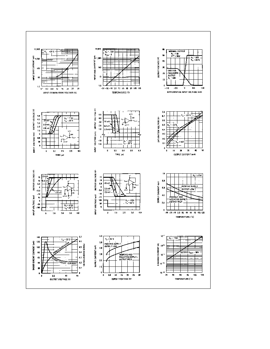
Typical Performance Characteristics
Input Bias Current
vs Common Mode
Input Bias Current
vs Temperature
Transfer Function
Response Time for Various
Input Overdrives
Response Time for Various
Input Overdrives
Output Saturation Voltage
Response Time for Various
Input Overdrives
Response Time for Various
Input Overdrives
Supply Current
Output Limiting Characteristics
Supply Current
Leakage Currents
TL H 5703 ≠ 4
4
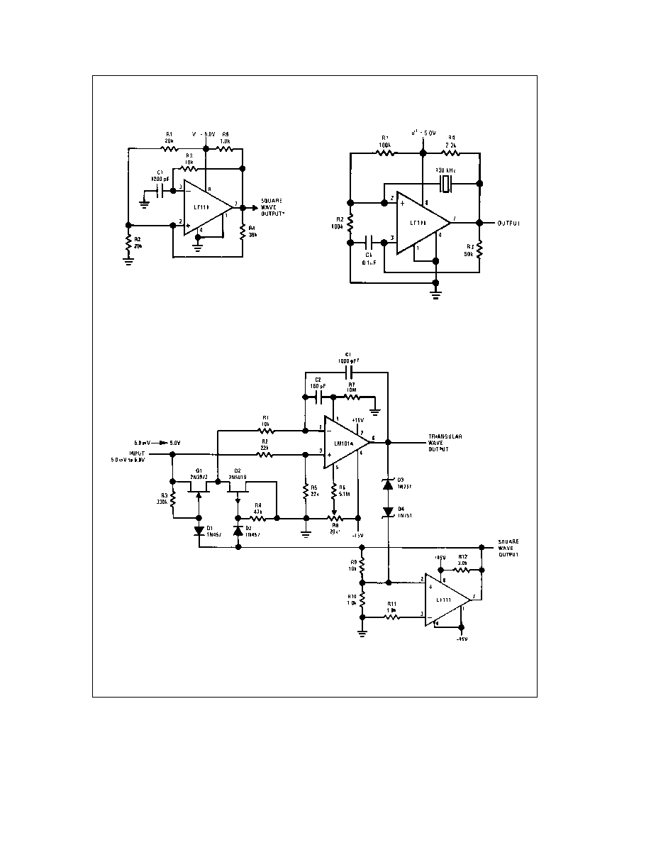
Typical Applications
100 kHz Free Running Multivibrator
TL H 5703 ≠ 7
TTL or DTL fanout of two
Crystal Oscillator
TL H 5703 ≠ 3
10 Hz to 10 kHz Voltage Controlled Oscillator
Adjust for symmetrical squarewave time when V
IN
e
5 0 mV
Minimum capacitance 20 pF Maximum frequency 50 kHz
TL H 5703 ≠ 5
5