TL H 9297
LF441
Low
Power
JFET
Input
Operational
Amplifier
February 1995
LF441 Low Power JFET
Input Operational Amplifier
General Description
The LF441 low power operational amplifier provides many
of the same AC characteristics as the industry standard
LM741 while greatly improving the DC characteristics of the
LM741 The amplifier has the same bandwidth slew rate
and gain (10 kX load) as the LM741 and only draws one
tenth the supply current of the LM741 In addition the well
matched high voltage JFET input devices of the LF441 re-
duce the input bias and offset currents by a factor of 10 000
over the LM741 A combination of careful layout design and
internal trimming guarantees very low input offset voltage
and voltage drift The LF441 also has a very low equivalent
input noise voltage for a low power amplifier
The LF441 is pin compatible with the LM741 allowing an
immediate 10 times reduction in power drain in many appli-
cations The LF441 should be used where low power
dissipation and good electrical characteristics are the major
considerations
Features
Y
1 10 supply current of a LM741
200 mA (max)
Y
Low input bias current
50 pA (max)
Y
Low input offset voltage
0 5 mV (max)
Y
Low input offset voltage drift
10 mV C (max)
Y
High gain bandwidth
1 MHz
Y
High slew rate
1 V ms
Y
Low noise voltage for low power
35 nV
S
Hz
Y
Low input noise current
0 01 pA
S
Hz
Y
High input impedance
10
12
X
Y
High gain V
O
e
g
10V R
L
e
10k
50k (min)
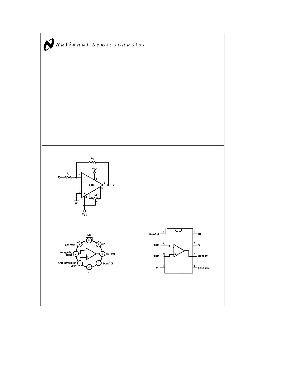
Typical Connection
TL H 9297 ≠ 1
Ordering Information
LF441XYZ
X
indicates electrical grade
Y
indicates temperature range
``M'' for military
``C'' for commercial
Z
indicates package type
``H'' or ``N''
Connection Diagrams
Metal Can Package
TL H 9297 ≠ 2
Top View
Note
Pin 4 connected to case
Order Number LF441MH 883
See NS Package Number H08A
Dual-In-Line Package
TL H 9297 ≠ 4
Top View
Order Number LF441ACN
LF441CM or LF441CN
See NS Package Number M08A or N08E
BI-FET
TM
is a trademark of National Semiconductor Corporation
C1995 National Semiconductor Corporation
RRD-B30M115 Printed in U S A
Absolute Maximum Ratings
If Military Aerospace specified devices are required
please contact the National Semiconductor Sales
Office Distributors for availability and specifications
LF441A
LF441
Supply Voltage
g
22V
g
18V
Differential Input Voltage
g
38V
g
30V
LF441A
LF441
Input Voltage Range
(Note 1)
g
19V
g
15V
Output Short Circuit
Duration
Continuous
Continuous
H Package
N Package
M Package
Power Dissipation
670 mW
670 mW
(Notes 2 and 9)
T
j max
150 C
115 C
i
jA
(Typical)
130 C W
185 C W
Board Mount in still air
165 C W
Board Mount in 400 LF
65 C W
min air flow
i
jC
25 C W
Operating Temp Range
(Note 3)
(Note 3)
Storage Temp Range
b
65 C
s
T
A
s
150 C
b
65 C
s
T
A
s
150 C
Lead Temperature
300 C
260 C
(Soldering 10 seconds)
LF441A
LF441
Soldering Information
Dual-In-Line Package
Soldering (10 sec )
260 C
260 C
Small Outline Package
Vapor Phase (60 sec )
215 C
215 C
Infrared (15 sec )
220 C
220 C
See AN-450 ``Surface Mounting Methods and Their Effect
on Product Reliability'' for other methods of soldering sur-
face mount devices
ESD Tolerance (Note 10)
Rating to be Determined
DC Electrical Characteristics
(Note 4)
Symbol
Parameter
Conditions
LF441A
LF441
Units
Min
Typ
Max
Min
Typ
Max
V
OS
Input Offset Voltage
R
S
e
10 kX T
A
e
25 C
0 3
0 5
1
5
mV
Over Temperature
7 5
mV
D
V
OS
D
T
Average TC of Input
R
S
e
10 kX (Note 5)
7
10
10
m
V C
Offset Voltage
I
OS
Input Offset Current
V
S
e
g
15V
T
j
e
25 C
5
25
5
50
pA
(Notes 4 and 6)
T
j
e
70 C
1 5
1 5
nA
T
j
e
125 C
10
nA
I
B
Input Bias Current
V
S
e
g
15V
T
j
e
25 C
10
50
10
100
pA
(Notes 4 and 6)
T
j
e
70 C
3
3
nA
T
j
e
125 C
20
nA
R
IN
Input Resistance
T
j
e
25 C
10
12
10
12
X
A
VOL
Large Signal Voltage
V
S
e
g
15V V
O
e
g
10V
50
100
25
100
V mV
Gain
R
L
e
10 kX T
A
e
25 C
Over Temperature
25
15
V mV
V
O
Output Voltage Swing
V
S
e
g
15V R
L
e
10 kX
g
12
g
13
g
12
g
13
V
V
CM
Input Common-Mode
g
16
a
18
b
17
g
11
a
14
b
12
V
Voltage Range
CMRR
Common-Mode
R
S
s
10 kX
80
100
70
95
dB
Rejection Ratio
2
DC Electrical Characteristics
(Note 4) (Continued)
Symbol
Parameter
Conditions
LF441A
LF441
Units
Min
Typ
Max
Min
Typ
Max
PSRR
Supply Voltage
(Note 7)
80
100
70
90
dB
Rejection Ratio
I
S
Supply Current
150
200
150
250
m
A
AC Electrical Characteristics
(Note 4)
Symbol
Parameter
Conditions
LF441A
LF441
Units
Min
Typ
Max
Min
Typ
Max
SR
Slew Rate
V
S
e
g
15V T
A
e
25 C
0 8
1
0 6
1
V ms
GBW
Gain-Bandwidth Product
V
S
e
g
15V T
A
e
25 C
0 8
1
0 6
1
MHz
e
n
Equivalent Input Noise Voltage
T
A
e
25 C R
S
e
100X
35
35
nV
0
Hz
f
e
1 kHz
i
n
Equivalent Input Noise Current
T
A
e
25 C f
e
1 kHz
0 01
0 01
pA
0
Hz
Note 1
Unless otherwise specified the absolute maximum negative input voltage is equal to the negative power supply voltage
Note 2
For operating at elevated temperature these devices must be derated based on a thermal resistance of i
jA
Note 3
The temperature range is designated by the position just before the package type in the device number A ``C'' indicates the commercial temperature range
and an ``M'' indicates the military temperature range The military temperature range is available in ``H'' package only
Note 4
Unless otherwise specified the specifications apply over the full temperature range and for V
S
e g
20V for the LF441A and for V
S
e g
15V for the LF441
V
OS
I
B
and I
OS
are measured at V
CM
e
0
Note 5
The LF441A is 100% tested to this specification
Note 6
The input bias currents are junction leakage currents which approximately double for every 10 C increase in the junction temperature T
j
Due to limited
production test time the input bias currents measured are correlated to junction temperature In normal operation the junction temperature rises above the ambient
temperature as a result of internal power dissipation P
D
T
j
e
T
A
a
i
jA
P
D
where i
jA
is the thermal resistance from junction to ambient Use of a heat sink is
recommended if input bias current is to be kept to a minimum
Note 7
Supply voltage rejection ratio is measured for both supply magnitudes increasing or decreasing simultaneously in accordance with common practice From
g
15V to
g
5V for the LF441 and from
g
20V to
g
5V for the LF441A
Note 8
Refer to RETS441X for LF441MH military specifications
Note 9
Max Power Dissipation is defined by the package characteristics Operating the part near the Max Power Dissipation may cause the part to operate
outside guaranteed limits
Note 10
Human body model 1 5 kX in series with 100 pF
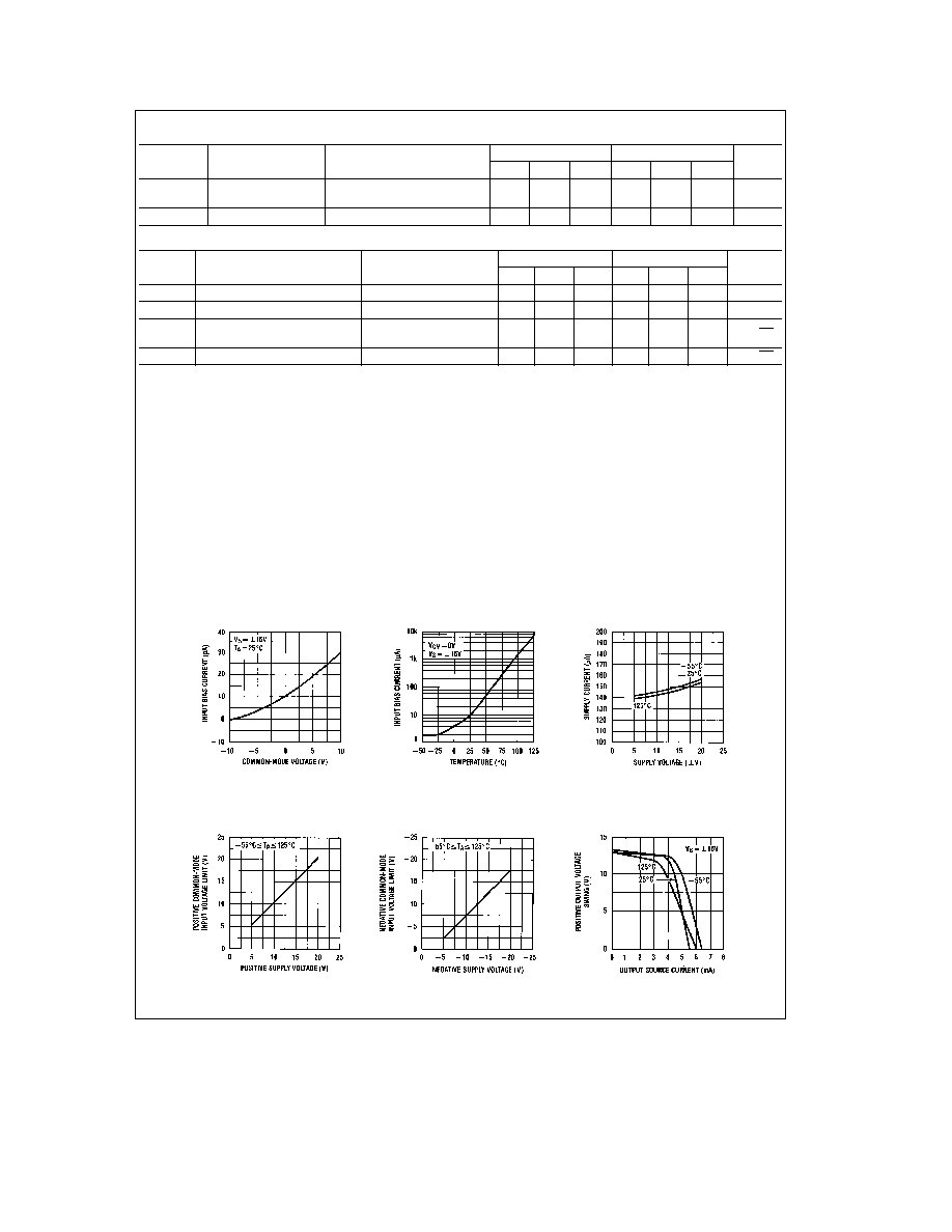
Typical Performance Characteristics
Input Bias Current
Input Bias Current
Supply Current
Input Voltage Limit
Positive Common-Mode
Input Voltage Limit
Negative Common-Mode
Positive Current Limit
TL H 9297 ≠ 5
3

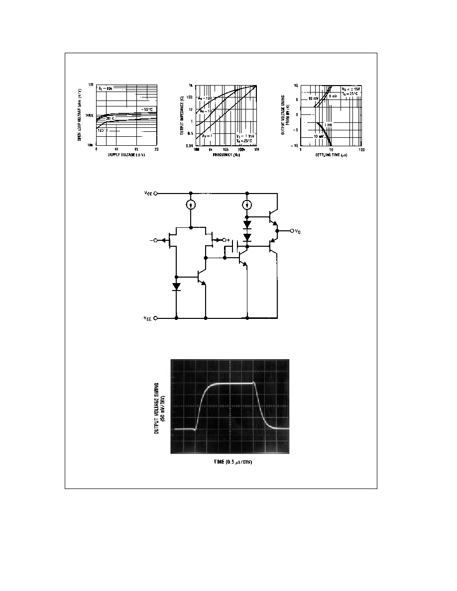
Typical Performance Characteristics
(Continued)
Negative Current Limit
Output Voltage Swing
Output Voltage Swing
Gain Bandwidth
Bode Plot
Slew Rate
Distortion vs Frequency
Voltage Swing
Undistorted Output
Open Loop Frequency
Response
Common-Mode
Rejection Ratio
Power Supply
Rejection Ratio
Equivalent Input
Noise Voltage
TL H 9297 ≠ 6
4