 | –≠–ª–µ–∫—Ç—Ä–æ–Ω–Ω—ã–π –∫–æ–º–ø–æ–Ω–µ–Ω—Ç: LF444 | –°–∫–∞—á–∞—Ç—å:  PDF PDF  ZIP ZIP |
LF444
Quad Low Power JFET Input Operational Amplifier
General Description
The LF444 quad low power operational amplifier provides
many of the same AC characteristics as the industry stan-
dard LM148 while greatly improving the DC characteristics
of the LM148. The amplifier has the same bandwidth, slew
rate, and gain (10 k
load) as the LM148 and only draws
one fourth the supply current of the LM148. In addition the
well matched high voltage JFET input devices of the LF444
reduce the input bias and offset currents by a factor of
10,000 over the LM148. The LF444 also has a very low
equivalent input noise voltage for a low power amplifier.
The LF444 is pin compatible with the LM148 allowing an im-
mediate 4 times reduction in power drain in many applica-
tions. The LF444 should be used wherever low power dissi-
pation and good electrical characteristics are the major
considerations.
Features
n
1
/
4
supply current of a LM148:
200 µA/Amplifier (max)
n
Low input bias current:
50 pA (max)
n
High gain bandwidth:
1 MHz
n
High slew rate:
1 V/µs
n
Low noise voltage for low power
n
Low input noise current
n
High input impedance:
10
12
n
High gain V
O
=
±
10V, R
L
= 10k: 50k (min)
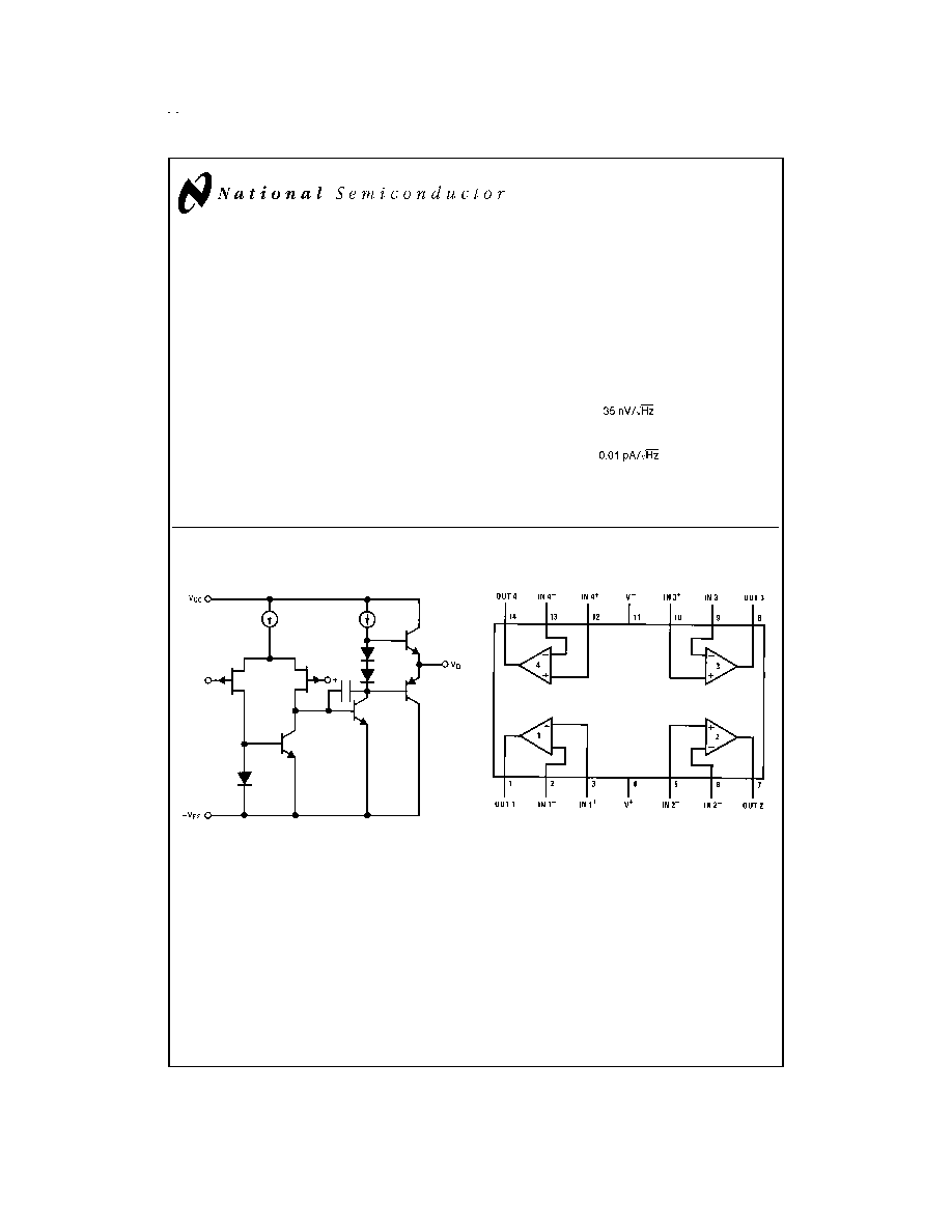
Simplified Schematic
Ordering Information
LF444XYZ
X indicates electrical grade
Y indicates temperature range
"M" for military, "C" for commercial
Z indicates package type "D", "M" or "N"
Connection Diagram
BI-FET
TM
and BI-FET II
TM
are trademarks of National Semiconductor Corporation.
1/4 Quad
DS009156-1
Dual-In-Line Package
DS009156-2
Top View
Order Number LF444AMD, LF444CM,
LF444ACN, LF444CN or LF444MD/883
See NS Package Number D14E, M14A or N14A
May 1998
LF444
Quad
Low
Power
JFET
Input
Operational
Amplifier
© 1999 National Semiconductor Corporation
DS009156
www.national.com
Absolute Maximum Ratings
(Note 11)
If Military/Aerospace specified devices are required,
please contact the National Semiconductor Sales Office/
Distributors for availability and specifications.
LF444A
LF444
Supply Voltage
±
22V
±
18V
Differential Input Voltage
±
38V
±
30V
Input Voltage Range
±
19V
±
15V
(Note 1)
Output Short Circuit
Continuous
Continuous
Duration (Note 2)
D Package
N, M Packages
Power Dissipation
900 mW
670 mW
(Notes 3, 9)
T
j
max
150∞C
115∞C
jA
(Typical)
100∞C/W
85∞C/W
LF444A/LF444
Operating Temperature Range
(Note 4)
Storage Temperature Range
-65∞C
T
A
150∞C
ESD Tolerance (Note 10)
Rating to
be determined
Soldering Information
Dual-In-Line Packages
(Soldering, 10 sec.)
260∞C
Small Outline Package
Vapor Phase (60 sec.)
215∞C
Infrared (15 sec.)
220∞C
See AN-450 "Surface Mounting Methods and Their Effect on
Product Reliability" for other methods of soldering surface
mount devices.
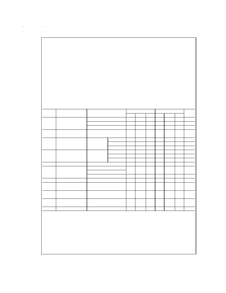
DC Electrical Characteristics
(Note 5)
Symbol
Parameter
Conditions
LF444A
LF444
Units
Min
Typ
Max
Min
Typ
Max
V
OS
Input Offset Voltage
R
S
= 10k, T
A
= 25∞C
2
5
3
10
mV
0∞C
T
A
+70∞C
6.5
12
mV
-55∞C
T
A
+125∞C
8
mV
V
OS
/
T
Average TC of Input
R
S
= 10 k
10
10
µV/∞C
Offset Voltage
I
OS
Input Offset Current
V
S
=
±
15V
T
j
= 25∞C
5
25
5
50
pA
(Notes 5, 6)
T
j
= 70∞C
1.5
1.5
nA
T
j
= 125∞C
10
nA
I
B
Input Bias Current
V
S
=
±
15V
T
j
= 25∞C
10
50
10
100
pA
(Notes 5, 6)
T
j
= 70∞C
3
3
nA
T
j
= 125∞C
20
nA
R
IN
Input Resistance
T
j
= 25∞C
10
12
10
12
A
VOL
Large Signal Voltage
V
S
=
±
15V, V
O
=
±
10V
50
100
25
100
V/mV
Gain
R
L
= 10 k
, T
A
= 25∞C
Over Temperature
25
15
V/mV
V
O
Output Voltage Swing
V
S
=
±
15V, R
L
= 10 k
±
12
±
13
±
12
±
13
V
V
CM
Input Common-Mode
±
16
+18
±
11
+14
V
Voltage Range
-17
-12
V
CMRR
Common-Mode
R
S
10 k
80
100
70
95
dB
Rejection Ratio
PSRR
Supply Voltage
(Note 7)
80
100
70
90
dB
Rejection Ratio
I
S
Supply Current
0.6
0.8
0.6
1.0
mA
www.national.com
2
AC Electrical Characteristics
(Note 5)
Symbol
Parameter
Conditions
LF444A
LF444
Units
Min
Typ
Max
Min
Typ
Max
Amplifier-to-Amplifier
-120
-120
dB
Coupling
SR
Slew Rate
V
S
=
±
15V, T
A
= 25∞C
1
1
V/µs
GBW
Gain-Bandwidth Product
V
S
=
±
15V, T
A
= 25∞C
1
1
MHz
e
n
Equivalent Input Noise Voltage
T
A
= 25∞C, R
S
= 100
,
35
35
f = 1 kHz
i
n
Equivalent Input Noise Current
T
A
= 25∞C, f = 1 kHz
0.01
0.01
Note 1: Unless otherwise specified the absolute maximum negative input voltage is equal to the negative power supply voltage.
Note 2: Any of the amplifier outputs can be shorted to ground indefinitely, however, more than one should not be simultaneously shorted as the maximum junction
temperature will be exceeded.
Note 3: For operating at elevated temperature, these devices must be derated based on a thermal resistance of
jA
.
Note 4: The LF444A is available in both the commercial temperature range 0∞C
T
A
70∞C and the military temperature range -55∞C
T
A
125∞C. The LF444 is
available in the commercial temperature range only. The temperature range is designated by the position just before the package type in the device number. A "C"
indicates the commercial temperature range and an "M" indicates the military temperature range. The military temperature range is available in "D" package only.
Note 5: Unless otherwise specified the specifications apply over the full temperature range and for V
S
=
±
20V for the LF444A and for V
S
=
±
15V for the LF444. V
OS
,
I
B
, and I
OS
are measured at V
CM
= 0.
Note 6: The input bias currents are junction leakage currents which approximately double for every 10∞C increase in the junction temperature, T
j
. Due to limited pro-
duction test time, the input bias currents measured are correlated to junction temperature. In normal operation the junction temperature rises above the ambient tem-
perature as a result of internal power dissipation, P
D
. T
j
= T
A
+
jA
P
D
where
jA
is the thermal resistance from junction to ambient. Use of a heat sink is recommended
if input bias current is to be kept to a minimum.
Note 7: Supply voltage rejection ratio is measured for both supply magnitudes increasing or decreasing simultaneously in accordance with common practice from
±
15V to
±
5V for the LF444 and from
±
20V to
±
5V for the LF444A.
Note 8: Refer to RETS444X for LF444MD military specifications.
Note 9: Max. Power Dissipation is defined by the package characteristics. Operating the part near the Max. Power Dissipation may cause the part to operate outside
guaranteed limits.
Note 10: Human body model, 1.5 k
in series with 100 pF.
Note 11: Absolute Maximum Ratings indicate limits beyond which damage to the device may occur. Operating ratings indicate conditions for which the device is func-
tional, but do not guarantee specific performance limits. Electrical Characteristics state DC and AC electrical specifications under particular test conditions which guar-
antee specific performance limits. This assumes that the device is within the Operating Ratings. Specifications are not guaranteed for parameters where no limit is
given, however, the typical value is a good indication of device performance.
Typical Performance Characteristics
Input Bias Current
DS009156-12
Input Bias Current
DS009156-13
Supply Current
DS009156-14
www.national.com
3
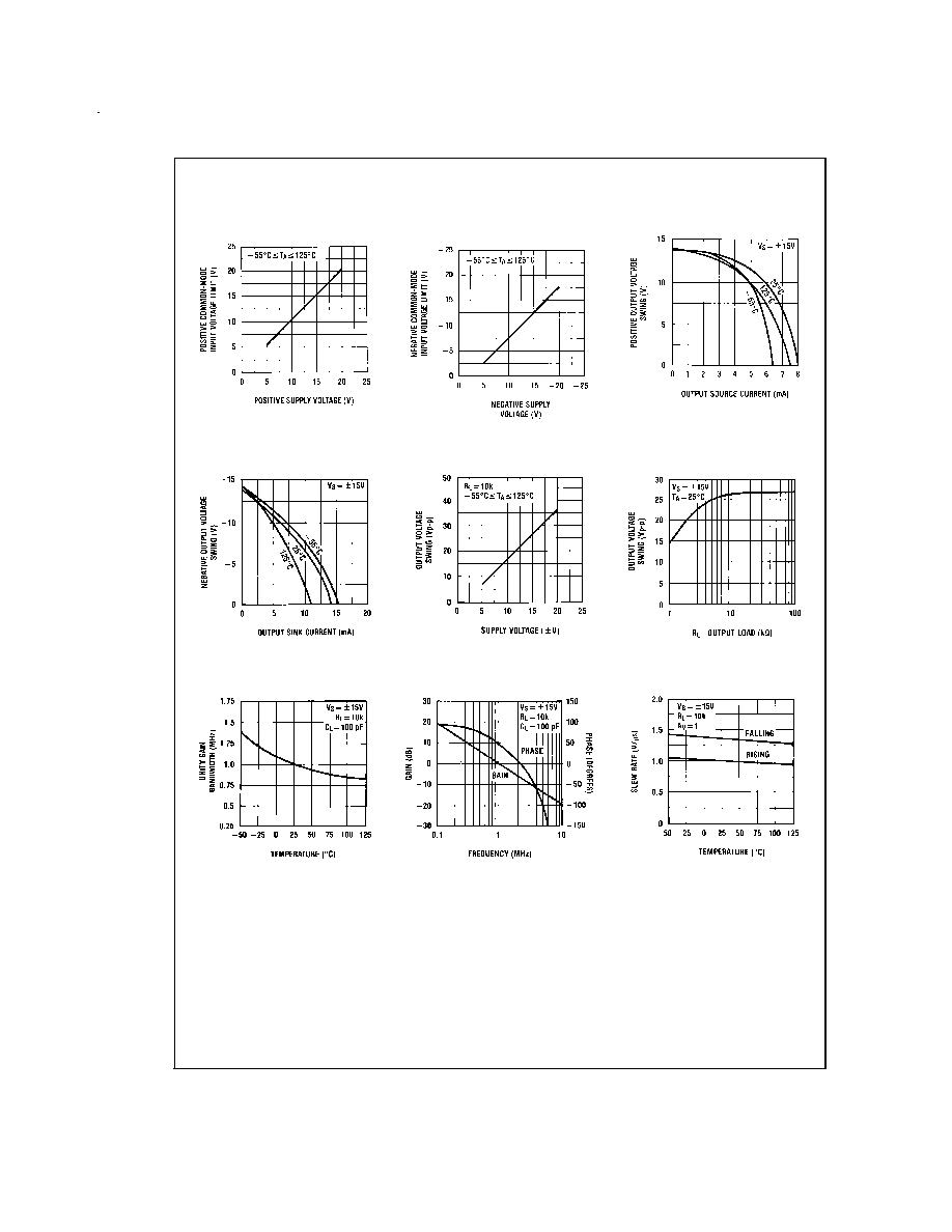
Typical Performance Characteristics
(Continued)
Positive Common-Mode
Input Voltage Limit
DS009156-15
Negative Common-Mode
Input Voltage Limit
DS009156-16
Positive Current Limit
DS009156-17
Negative Current Limit
DS009156-18
Output Voltage Swing
DS009156-19
Output Voltage Swing
DS009156-20
Gain Bandwidth
DS009156-21
Bode Plot
DS009156-22
Slew Rate
DS009156-23
www.national.com
4
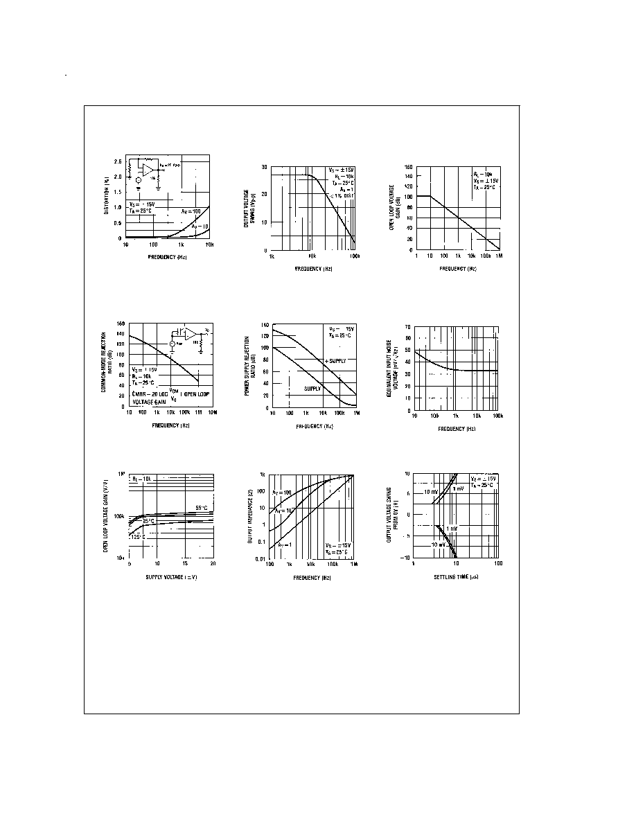
Typical Performance Characteristics
(Continued)
Distortion vs Frequency
DS009156-24
Undistorted Output
Voltage Swing
DS009156-25
Open Loop
Frequency Response
DS009156-26
Common-Mode
Rejection Ratio
DS009156-27
Power Supply
Rejection Ratio
DS009156-28
Equivalent Input
Noise Voltage
DS009156-29
Open Loop Voltage Gain
DS009156-30
Output Impedance
DS009156-31
Inverter Settling Time
DS009156-32
www.national.com
5
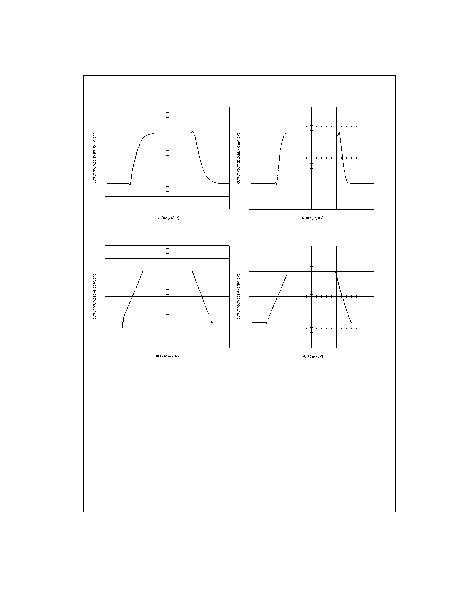
Pulse Response
R
L
= 10 k
, C
L
= 10 pF
Application Hints
This device is a quad low power op amp with JFET input de-
vices ( BI-FET
TM
). These JFETs have large reverse break-
down voltages from gate to source and drain eliminating the
need for clamps across the inputs. Therefore, large differen-
tial input voltages can easily be accommodated without a
large increase in input current. The maximum differential in-
put voltage is independent of the supply voltages. However,
neither of the input voltages should be allowed to exceed the
negative supply as this will cause large currents to flow
which can result in a destroyed unit.
Exceeding the negative common-mode limit on either input
will force the output to a high state, potentially causing a re-
versal of phase to the output. Exceeding the negative
common-mode limit on both inputs will force the amplifier
output to a high state. In neither case does a latch occur
since raising the input back within the common-mode range
again puts the input stage and thus the amplifier in a normal
operating mode.
Exceeding the positive common-mode limit on a single input
will not change the phase of the output; however, if both in-
puts exceed the limit, the output of the amplifier will be forced
to a high state.
The amplifiers will operate with a common-mode input volt-
age equal to the positive supply; however, the gain band-
width and slew rate may be decreased in this condition.
When the negative common-mode voltage swings to within
3V of the negative supply, an increase in input offset voltage
may occur.
Each amplifier is individually biased to allow normal circuit
operation with power supplies of
±
3.0V. Supply voltages less
than these may degrade the common-mode rejection and re-
strict the output voltage swing.
The amplifiers will drive a 10 k
load resistance to
±
10V
over the full temperature range. If the amplifier is forced to
drive heavier load currents, however, an increase in input
offset voltage may occur on the negative voltage swing and
finally reach an active current limit on both positive and
negative swings.
Small Signal Inverting
DS009156-6
Small Signal Non-Inverting
DS009156-7
Large Signal Inverting
DS009156-8
Large Signal Non-Inverting
DS009156-9
www.national.com
6
Application Hints
(Continued)
Precautions should be taken to ensure that the power supply
for the integrated circuit never becomes reversed in polarity
or that the unit is not inadvertently installed backwards in a
socket as an unlimited current surge through the resulting
forward diode within the IC could cause fusing of the internal
conductors and result in a destroyed unit.
As with most amplifiers, care should be taken with lead
dress, component placement and supply decoupling in order
to ensure stability. For example, resistors from the output to
an input should be placed with the body close to the input to
minimize "pick-up" and maximize the frequency of the feed-
back pole by minimizing the capacitance from the input to
ground.
A feedback pole is created when the feedback around any
amplifier is resistive. The parallel resistance and capacitance
from the input of the device (usually the inverting input) to AC
ground set the frequency of the pole. In many instances the
frequency of this pole is much greater than the expected 3
dB frequency of the closed loop gain and consequently there
is negligible effect on stability margin. However, if the feed-
back pole is less than approximately 6 times the expected 3
dB frequency a lead capacitor should be placed from the out-
put to the input of the op amp. The value of the added ca-
pacitor should be such that the RC time constant of this ca-
pacitor and the resistance it parallels is greater than or equal
to the original feedback pole time constant.
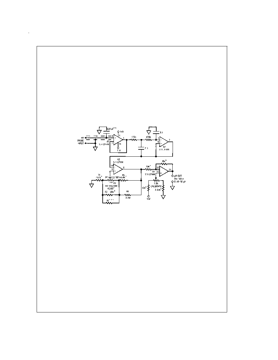
Typical Application
pH Probe Amplifier/Temperature Compensator
DS009156-10
***
For R2 = 50k, R4 = 330k
±
1%
For R2 = 100k, R4 = 75k
±
1%
For R2 = 200k, R4 = 56k
±
1%
**
Polystyrene
*
Film resistor type RN60C
To calibrate, insert probe in pH =7 solution. Set the "TEMPERATURE ADJUST" pot, R2, to correspond to the solution temperature: full clockwise for 0∞C, and
proportionately for intermediate temperatures, using a turns-counting dial. Then set "CALIBRATE" pot so output reads 7V.
Typical probe = Ingold Electrodes #465-35
www.national.com
7

Detailed Schematic
1/4 Quad
DS009156-11
www.national.com
8

Physical Dimensions
inches (millimeters) unless otherwise noted
Order Number LF444AMD or LF444MD/883
See NS Package Number D14E
Order Number LF444CM
See NS Package Number M14A
www.national.com
9

Physical Dimensions
inches (millimeters) unless otherwise noted (Continued)
LIFE SUPPORT POLICY
NATIONAL'S PRODUCTS ARE NOT AUTHORIZED FOR USE AS CRITICAL COMPONENTS IN LIFE SUPPORT
DEVICES OR SYSTEMS WITHOUT THE EXPRESS WRITTEN APPROVAL OF THE PRESIDENT OF NATIONAL
SEMICONDUCTOR CORPORATION. As used herein:
1. Life support devices or systems are devices or
systems which, (a) are intended for surgical implant
into the body, or (b) support or sustain life, and
whose failure to perform when properly used in
accordance with instructions for use provided in the
labeling, can be reasonably expected to result in a
significant injury to the user.
2. A critical component is any component of a life
support device or system whose failure to perform
can be reasonably expected to cause the failure of
the life support device or system, or to affect its
safety or effectiveness.
National Semiconductor
Corporation
Americas
Tel: 1-800-272-9959
Fax: 1-800-737-7018
Email: support@nsc.com
National Semiconductor
Europe
Fax: +49 (0) 1 80-530 85 86
Email: europe.support@nsc.com
Deutsch Tel: +49 (0) 1 80-530 85 85
English
Tel: +49 (0) 1 80-532 78 32
FranÁais Tel: +49 (0) 1 80-532 93 58
Italiano
Tel: +49 (0) 1 80-534 16 80
National Semiconductor
Asia Pacific Customer
Response Group
Tel: 65-2544466
Fax: 65-2504466
Email: sea.support@nsc.com
National Semiconductor
Japan Ltd.
Tel: 81-3-5639-7560
Fax: 81-3-5639-7507
www.national.com
Order Number LF444ACN or LF444CN
See NS Package Number N14A
LF444
Quad
Low
Power
JFET
Input
Operational
Amplifier
National does not assume any responsibility for use of any circuitry described, no circuit patent licenses are implied and National reserves the right at any time without notice to change said circuitry and specifications.