 | –≠–ª–µ–∫—Ç—Ä–æ–Ω–Ω—ã–π –∫–æ–º–ø–æ–Ω–µ–Ω—Ç: LF6197 | –°–∫–∞—á–∞—Ç—å:  PDF PDF  ZIP ZIP |
TL H 11381
LF6197
160
ns
Monolithic
Sample-and-Hold
Amplifier
September 1992
LF6197 160 ns Monolithic Sample-and-Hold Amplifier
General Description
The LF6197 is a monolithic sample-and-hold (S H) amplifier
that uses a proprietary ``current-multiplexed sample-and-
hold'' technique to offer extremely high speed while main-
taining 12 bits or higher accuracy The device is built using
National's advanced junction-isolated VIP
TM
(Vertically Inte-
grated PNP) and BI-FET
TM
process technologies
The LF6197 acquires a 10V step input to within
g
0 01% in
160 ns and has 10 mV hold step error when going from
sample to hold mode The input offset voltage in the sample
mode is typically 3 mV Even at extremely fast acquisition
speeds no compromises are made in the droop rate which
is 0 6 mV ms When configured for unity gain the DC gain
error is 0 03% The feedthrough attenuation in the hold
mode is 83 dB at DC and 77 dB at 100 kHz
The LF6197 can be externally configured for either inverting
or non-inverting gains thus offering additional flexibility to
the user The device includes an internal 10 pF hold capaci-
tor
BI-FET
TM
and VIP
TM
are trademarks of National Semiconductor Corporation
Features
Y
Operates with supply voltages from
g
5V to
g
18V
Y
CMOS TTL and ECL compatible logic input
Y
Adjustable inverting or non-inverting gain
Y
Internal hold capacitor
Y
High power-supply rejection in both sample and hold
modes
Key Specifications
Y
Acquisition time (10V step to 0 01%)
160 ns
Y
Hold mode settling time (10V step to 0 01%)
50 ns
Y
Droop rate
0 6 mV ms
Y
Hold step
10 mV
Y
Aperture jitter
8 ps
rms
Y
Feedthrough attenuation at DC
83 dB
Y
Small signal bandwidth
25 MHz
Applications
Y
High-speed data acquisition systems
Y
Automatic test equipment
Y
High-speed instrumentation
Y
Replaces expensive hybrid sample-and-hold amplifiers
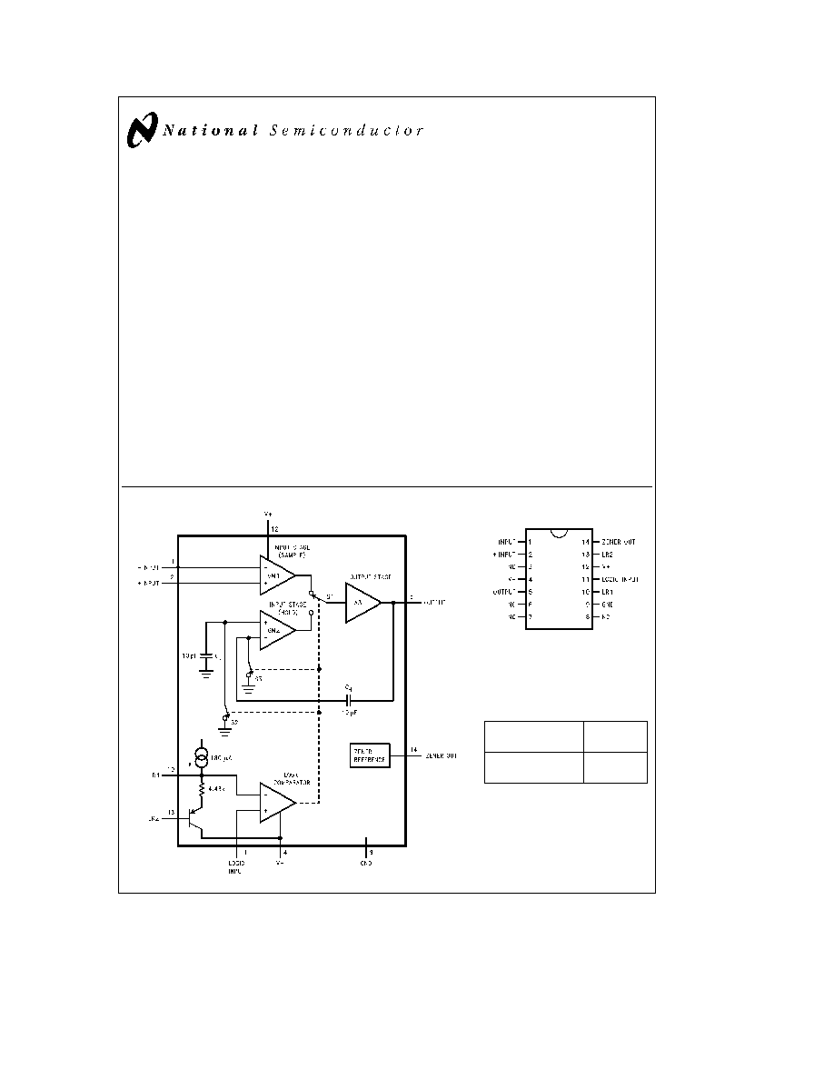
Block Diagram
TL H 11381 ≠ 1
Connection Diagram
TL H 11381 ≠ 2
Top View
Ordering Information
Industrial
Package
(0 C
k
T
A
k
a
70 C)
LF6197CCJ
J14A
Ceramic DIP
C1995 National Semiconductor Corporation
RRD-B30M115 Printed in U S A
Absolute Maximum Ratings
(Notes 1 2)
Positive Supply Voltage (V
a
)
a
18V
Negative Supply Voltage (V
b
)
b
18V
Analog Input Voltage
V
a
or V
b
or
g
12 5V
whichever is less
Logic Input to LR1 Differential Voltage
g
5V
Power Dissipation (Note 3)
1 2W
Duration of Output Short Circuit to GND
(Note 4)
ESD Susceptibility
All Pins except Pin 13 (Note 5)
2000V
Pin 13 only (Note 5)
1500V
Lead Temperature (Soldering 10 sec )
J Package
300 C
Storage Temperature
b
65 C to
a
150 C
Operating Ratings
(Notes 1 2)
Temperature Range
T
MIN
s
T
A
s
T
MAX
LF6197CCJ
0 C
s
T
A
s
a
70 C
Positive Supply Voltage
a
4 75V
s
V
a s
a
15 75V
Negative Supply Voltage
b
15 75V
s
V
b s
b
4 75V
Electrical Characteristics
Unless otherwise specified the following specifications apply for V
a
e
a
15V V
b
e
b
15V
b
12V
s
V
IN
s
a
12V
R
L
l
1 kX C
L
s
40 pF Logic Reference 2 (LR2) voltage
e
0V and Logic Input Voltage
k
1 4V threshold (Unit is in ``sample''
mode) V
S
refers to the supply voltages V
a
and V
b
Boldface limits apply for T
A
e
T
J
from T
MIN
to T
MAX
all other limits
T
A
e
T
J
e
25 C
Symbol
Parameter
Conditions
Typical
Limit
Units
(Note 6)
(Note 7)
(Limit)
INPUT CHARACTERISTICS
V
OS
Input Offset Voltage
g
3 0
g
6 0
mV (max)
V
S
e
g
5V (Note 8)
g
3 0
mV (max)
D
V
OS
D
T
Input Offset Drift
15
m
V C
R
IN com
Input Resistance (common mode)
10
MX
R
IN dif
Input Resistance (differential)
300
kX
CMRR
Common Mode Rejection Ratio
V
CM
e
g
10V
100
80
dB (min)
I
Ba
Positive Input Bias Current
7
17
m
A (max)
I
Bb
Negative Input Bias Current
1
7 5
m
A (max)
TRANSFER CHARACTERISTICS
DC Open Loop Gain
V
OUT
e
g
12V R
L
e
1 kX
70
65
dB (min)
DC Open Loop Gain (Note 8)
V
S
e
g
5V V
OUT
e
g
2 5V
55
49
dB (min)
Gain Error (Note 9)
0 03
% (max)
Gain Linearity Error
V
OUT
e
g
10V
0 003
0 0045
% (max)
f
u
Gain Bandwidth Product
25
14
MHz (min)
OUTPUT CHARACTERISTICS
R
OUT
Output Resistance
0 02
X
SR
Slew Rate
145
V ms
Short Circuit Source Current
b
63
b
25
mA (min)
Short Circuit Sink Current
70
25
mA (min)
C
L
Maximum Capacitive Load
No Oscillation
200
pF
2
Electrical Characteristics
(Continued)
Unless otherwise specified the following specifications apply for V
a
e
a
15V V
b
e
b
15V
b
12V
s
V
IN
s
a
12V
R
L
l
1 kX C
L
s
40 pF Logic Reference 2 (LR2) voltage
e
0V and Logic Input Voltage
k
1 4V threshold (Unit is in ``sample''
mode) V
S
refers to the supply voltages V
a
and V
b
Boldface limits apply for T
A
e
T
J
from T
MIN
to T
MAX
all other limits
T
A
e
T
J
e
25 C
Symbol
Parameter
Conditions
Typical
Limit
Units
(Note 6)
(Note 7)
(Limit)
SAMPLE HOLD CHARACTERISTICS
t
ACQ
Acquisition Time
to 0 1% (Note 10)
10V step
130
ns
to 0 01% (Note 10)
a
10V step
145
240
ns (max)
260
ns (max)
b
10V step
160
240
ns (max)
260
ns (max)
t
AD
Aperture Delay Time
4
ns
t
AJ
Aperture Jitter
8
ps
rms
Droop Rate
0 6
10
m
V ms (max)
V
HS
Hold Step (Note 11)
g
10
mV (max)
t
HMS
Hold Mode Settling Time to 0 01%
10V step
50
ns
Feedthrough Attenuation (Note 12)
f
e
1 kHz V
IN
e
20 V
p-p
83
80
dB (min)
f
e
100 kHz V
IN
e
20 V
p-p
77
dB
DYNAMIC CHARACTERISTICS
THD
Total Harmonic Distortion
f
e
10 kHz V
IN
e
20 V
p-p
b
83
dB
f
e
150 kHz V
IN
e
20 V
p-p
b
78
dB
FPBW
Full Power Bandwidth (Note 13)
V
IN
e
20 V
p ≠ p
2 3
MHz
Small Signal Bandwidth
25
MHz
DIGITAL LOGIC CHARACTERISTICS
V
IN(1)
Logical ``1'' Input Voltage
2 0
V (min)
V
IN(0)
Logical ``0'' Input Voltage
0 8
V (max)
Logic Input Current
6
20
m
A (max)
Logic Reference 2 Input Current
3
5
m
A (max)
Differential Logic Threshold
1 4
1 1
V(min)
(Logic Input to LR1)
1 6
V(max)
POWER SUPPLY CHARACTERISTICS
I
Sa
Positive Supply Current
20
30
mA (max)
I
Sa
Positive Supply Current
V
S
e
g
5V (Note 8)
18 2
27
mA (max)
I
Sb
Negative Supply Current
20
30
mA (max)
I
Sb
Negative Supply Current
V
S
e
g
5V (Note 8)
17 5
27
mA (max)
PSRR
Power Supply Rejection Ratio
V
S
e
g
12V to
g
16V
84
74
dB (min)
3

Electrical Characteristics
(Continued)
Note 1
Absolute Maximum Ratings indicate limits beyond which damage to the device may occur
Note 2
Operating Ratings indicate conditions for which the device is functional but do not guarantee specific performance limits For guaranteed specifications
and test conditions see the Electrical Characteristics The guaranteed specifications apply only for the test conditions listed Some performance characteristics
may degrade when the device is not operated under the listed test conditions
Note 3
The maximum power dissipation must be derated at elevated temperatures and is dictated by T
Jmax
H
JA
and the ambient temperature T
A
The maximum
allowable power dissipation is P
D
e
(T
Jmax
b
T
A
) H
JA
or the number given in the Absolute Maximum Ratings whichever is lower For this device T
Jmax
e
150 C
and i
JA
e
125 C W The Power Derating Curve shows the safe thermal operating area for this device
Note 4
Continuous short-circuit operation at elevated ambient temperature can result in exceeding the maximum allowed junction temperature of 150 C
Note 5
Human body model 100 pF capacitor discharged through a 1 5 kX resistor
Note 6
Typicals are at T
A
e
25 C and represent the most likely parametric norm
Note 7
Limits are guaranteed to National's AOQL (Average Outgoing Quality Level)
Note 8
Operation at
g
5V requires that pin 14 be forced to 2 5V
Note 9
Gain error is calculated from the measured open loop gain
Note 10
The acquisition time of the LF6197 has been measured when the device has been configured as an inverting amplifier with a gain of
b
1 feedback
resistor of 2 kX feedback capacitor of 1 pF and a total load resistor of 1 kX
Note 11
Hold step is measured with the LF6197 configured as a unity gain follower and input connected to ground A TTL pulse with 4 ns rise and fall times is
applied to the logic input the hold step is dependent on the slew rate of the logic input pulse
Note 12
See test circuit
Figure 1
Note 13
Full power bandwidth is calculated using FPBW
e
SR (2qV
P
) where SR is the measured slew rate and V
P
is the peak voltage
4
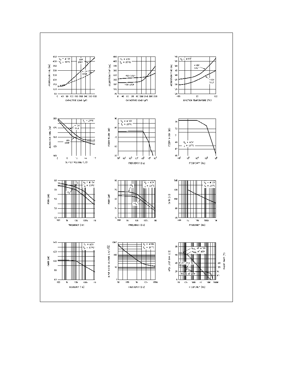
Typical Performance Characteristics
vs Capacitive Load
Acquisition Time (to 0 01%)
vs Capacitive Load
Acquisition Time (to 0 01%)
vs Temperature
Acquisition Time (to 0 01%)
vs Supply Voltage
Acquisition Time (to 0 01%)
vs Frequency
Signal Feedthrough
vs Frequency
Signal Feedthrough
Ratio vs Frequency
Power Supply Rejection
Ratio vs Frequency
Power Supply Rejection
Ratio vs Frequency
Common Mode Rejection
Ratio vs Frequency
Common Mode Rejection
vs Frequency
Input Noise Voltage
Response
Open Loop Frequency
TL H 11381 ≠ 3
5