 | –≠–ª–µ–∫—Ç—Ä–æ–Ω–Ω—ã–π –∫–æ–º–ø–æ–Ω–µ–Ω—Ç: LH0022C | –°–∫–∞—á–∞—Ç—å:  PDF PDF  ZIP ZIP |
TL K 5557
LH0042
Low
Cost
FET
Op
Amp
February 1995
LH0042
Low Cost FET Op Amp
General Description
The LH0042 is a FET input operational amplifier with very
high input impedance and low input currents with no com-
promise in noise common mode rejection ratio open loop
gain or slew rate The LH0042 is internally compensated
and is free of latch-up
The LH0042 is specified for operation over the
b
55 C to
a
125 C military temperature range The LH0042C is speci-
fied for operation over the
b
25 C to
a
85 C temperature
range
The LH0042 op amp is intended to fulfill a wide variety of
applications for process control medical instrumentation
and other systems requiring very low input currents The
LH0042 provides low cost high performance for such appli-
cations as electrometer and photocell amplification pico-
ammeters and high input impedance buffers
Features
Y
High open loop gain
100 dB typ
Y
Internal compensation
Y
Pin compatible with standard IC op amps
(TO-99 package)
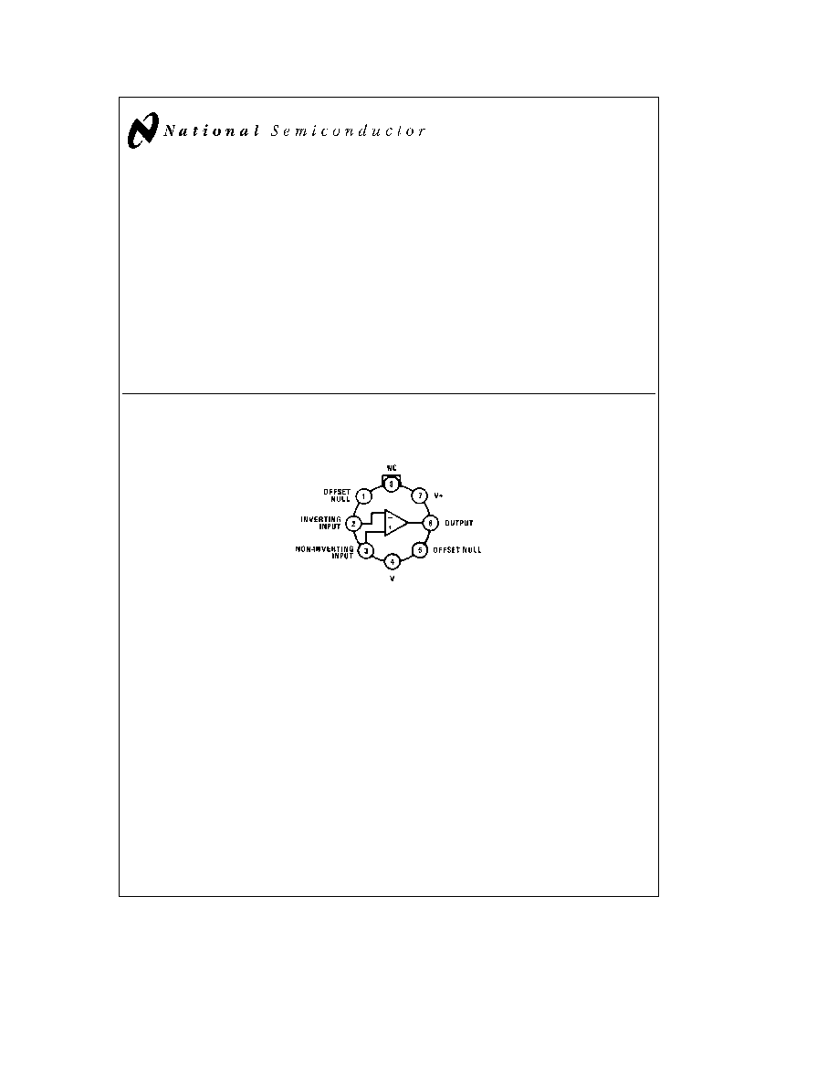
Connection Diagram
Metal Can Package
TL K 5557 ≠ 3
Top View
Order Number LH0042H-MIL LH0042H or LH0042CH
See NS Package Number H08D
C1995 National Semiconductor Corporation
RRD-B30M115 Printed in U S A
Absolute Maximum Ratings
If Military Aerospace specified devices are required
please contact the National Semiconductor Sales
Office Distributors for availability and specifications
Supply Voltage
g
22V
Power Dissipation (see Graph)
500 mW
Input Voltage (Note 1)
g
15V
Differential Input Voltage (Note 2)
g
30V
Voltage Between Offset Null and V
b
g
0 5V
Short Circuit Duration
Continuous
Operating Temperature Range
LH0022 LH0042 LH0052
b
55 C to
a
125 C
LH0022C LH0042C LH0052C
b
25 C to
a
85 C
Storage Temperature Range
b
65 C to
a
150 C
Lead Temperature (Soldering 10 sec )
300 C
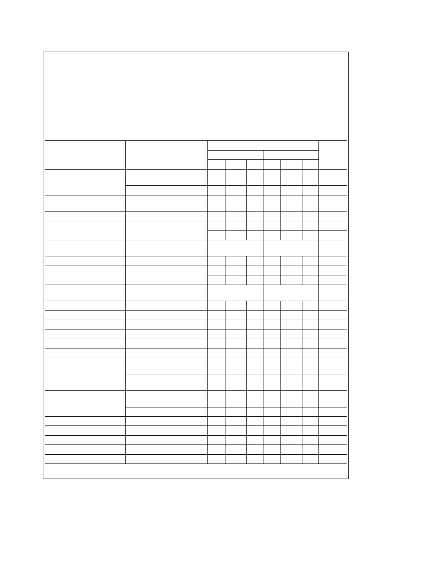
DC Electrical Characteristics
for LH0022 LH0022C (Note 3) T
A
e
T
J
(Max)
Limits
Parameter
Conditions
LH0022
LH0022C
Units
Min
Typ
Max
Min
Typ
Max
Input Offset Voltage
R
S
s
100 kX T
A
e
25 C
2 0
4 0
3 5
6 0
mV
V
S
e
g
15V
R
S
s
100 kX V
S
e
g
15V
5 0
7 0
mV
Temperature Coefficient of
R
S
s
100 kX
10
15
m
V C
Input Offset Voltage
Offset Voltage Drift with Time
3
4
m
V week
Input Offset Current
T
A
e
25 C (Note 4)
0 2
2 0
1 0
5 0
pA
2 0
0 5
nA
Temperature Coefficient of
Doubles Every 10 C
Doubles Every 10 C
Input Offset Current
Offset Current Drift with Time
0 1
0 1
pA week
Input Bias Current
T
A
e
25 C (Note 4)
5
10
10
25
pA
10
2 5
nA
Temperature Coefficient of
Doubles Every 10 C
Doubles Every 10 C
Input Bias Current
Differential Input Resistance
10
12
10
12
X
Common Mode Input Resistance
10
12
10
12
X
Input Capacitance
4 0
4 0
pF
Input Voltage Range
V
S
e
g
15V
g
12
g
13 5
g
12
g
13 5
V
Common Mode Rejection Ratio
R
S
s
10 kX V
IN
e
g
10V
74
90
70
90
dB
Supply Voltage Rejection Ratio
R
S
s
10 kX
g
5V
s
V
S
s g
15V
74
90
70
90
dB
Large Signal Voltage Gain
R
L
e
2 kX V
OUT
e
g
10V
75
100
75
100
V mV
T
A
e
25 C V
S
e
g
15V
R
L
e
2 kX V
OUT
e
g
10V
30
30
V mV
V
S
e
g
15V
Output Voltage Swing
R
L
e
1 kX T
A
e
25 C
g
10
g
12 5
g
10
g
12
V
V
S
e
g
15V
R
L
e
2 kX V
S
e
g
15V
g
10
g
10
V
Output Current Swing
V
OUT
e
g
10V T
A
e
25 C
g
10
g
15
g
10
g
15
mA
Output Resistance
75
75
X
Output Short Circuit Current
25
25
mA
Supply Current
V
S
e
g
15V
2 0
2 5
2 4
2 8
mA
Power Consumption
V
S
e
g
15V
75
85
mW
2
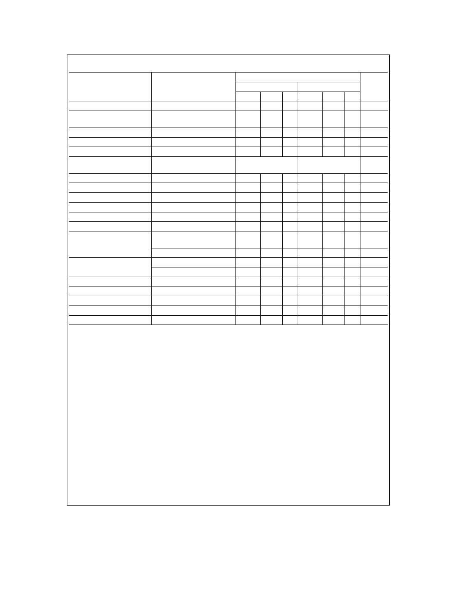
DC Electrical Characteristics
for LH0042 LH0042C (Note 3)
Limits
Parameter
Conditions
LH0042
LH0042C
Units
Min
Typ
Max
Min
Typ
Max
Input Offset Voltage
R
S
s
100 kX
5 0
20
6 0
20
mV
Temperature Coefficient of
R
S
s
100 kX
10
15
m
V C
Input Offset Voltage
Offset Voltage Drift with Time
7 0
10
m
V week
Input Offset Current
T
A
e
25 C (Note 4)
1 0
5 0
2 0
10
pA
Input Bias Current
T
A
e
25 C (Note 4)
10
25
15
50
pA
Temperature Coefficient of
Doubles Every 10 C
Doubles Every 10 C
Input Bias Current
Differential Input Resistance
10
12
10
12
X
Common Mode Input Resistance
10
12
10
12
X
Input Capacitance
4 0
4 0
pF
Input Voltage Range
g
12
g
13 5
g
12
g
13 5
V
Common Mode Rejection Ratio
R
S
s
10 kX V
IN
e
g
10V
70
86
70
80
dB
Supply Voltage Rejection Ratio
R
S
s
10 kX
g
5V
s
V
S
s g
15V
70
86
70
86
dB
Large Signal Voltage Gain
R
S
s
2 kX V
OUT
e
g
10V
50
100
25
100
V mV
T
A
e
25 C
R
S
s
2 kX V
OUT
e
g
10V
30
25
V mV
Output Voltage Swing
R
L
e
1 kX T
A
e
25 C
g
10
g
12 5
g
10
g
12
V
R
L
e
2 kX
g
10
g
10
V
Output Current Swing
V
OUT
e
g
10V
g
10
g
15
g
10
g
15
mA
Output Resistance
75
75
X
Output Short Circuit Current
20
20
mA
Supply Current
V
S
e
g
15V
2 5
3 5
2 8
4 0
mA
Power Consumption
V
S
e
g
15V
105
120
mW
3
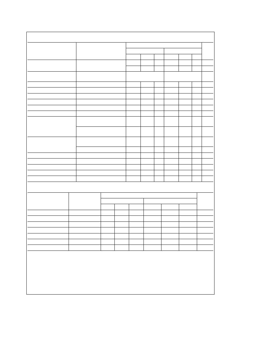
DC Electrical Characteristics
for LH0052 LH0052C (Note 3) (Continued)
Limits
Parameter
Conditions
LH0052
LH0052C
Units
Min
Typ
Max
Min
Typ
Max
Input Bias Current
T
A
e
25 C (Note 4)
0 5
2 5
1 0
5 0
pA
2 5
0 5
nA
Temperature Coefficient of
Doubles Every 10 C
Doubles Every 10 C
Input Bias Current
Differential Input Resistance
10
12
10
12
X
Common Mode Input Resistance
10
12
10
12
X
Input Capacitance
4 0
4 0
pF
Input Voltage Range
V
S
e
g
15V
g
12
g
13 5
g
12
g
13 5
V
Common Mode Rejection Ratio
R
S
s
10 kX V
IN
e
g
10V
74
90
70
90
dB
Supply Voltage Rejection Ratio
R
S
s
10 kX
g
5V
s
V
S
s g
15V
74
90
70
90
dB
Large Signal Voltage Gain
R
L
e
2 kX V
OUT
e
g
10V
75
100
75
100
V mV
V
S
e
g
15V T
A
e
25 C
R
L
e
2 kX V
OUT
e
g
10V
30
30
V mV
V
S
e
g
15V
Output Voltage Swing
R
L
e
1 kX T
A
e
25 C
g
10
g
12 5
g
10
g
12
V
V
S
e
g
15V
R
L
e
2 kX V
S
e
g
15V
g
10
g
10
V
Output Current Swing
V
OUT
e
g
10V T
A
e
25 C
g
10
g
15
g
10
g
15
mA
Output Resistance
75
75
X
Output Short Circuit Current
25
25
mA
Supply Current
V
S
e
g
15V
3 0
3 5
3 0
3 8
mA
Power Consumption
V
S
e
g
15V
105
114
mW
AC Electrical Characteristics
for all amplifiers (T
A
e
25 C V
S
e
g
15V)
Limits
Parameter
Conditions
LH0022 42 52
LH0022C 42C 52C
Units
Min
Typ
Max
Min
Typ
Max
Slew Rate
Voltage Follower
1 5
3 0
1 0
3 0
V ms
Large Signal Bandwidth
Voltage Follower
40
40
kHz
Small Signal Bandwidth
1 0
1 0
MHz
Rise Time
0 3
1 5
0 3
1 5
m
s
Overshoot
10
30
15
40
%
Settling Time (0 1%)
D
V
IN
e
10V
4 5
4 5
m
s
Overload Recovery
4 0
4 0
m
s
4
AC Electrical Characteristics
for all amplifiers (T
A
e
25 C V
S
e
g
15V) (Continued)
Limits
Parameter
Conditions
LH0042
LH0042C
Units
Min
Typ
Max
Min
Typ
Max
Input Noise Voltage
R
S
e
10 kX f
o
e
10 Hz
150
150
nV
S
Hz
R
S
e
10 kX f
o
e
100 Hz
55
55
nV
S
Hz
R
S
e
10 kX f
o
e
1 kHz
35
35
nV
S
Hz
R
S
e
10 kX f
o
e
10 kHz
30
30
nV
S
Hz
BW
e
10 Hz to 10kHz R
S
e
10 kX
12
12
m
Vrms
Note 1
For supply voltages less than
g
15V the absolute maximum input voltage is equal to the supply voltage
Note 2
Rating applies for minimum source resistance of 10 kX for source resistances less than 10 kX maximum differential input voltage is
g
5V
Note 3
Unless otherwise specified these specifications apply for
g
5V
s
V
S
s g
20V and
b
55 C
s
T
A
s a
125 C for the LH0042 and
b
25 C
s
T
A
s a
85 C
for the LH0042C Typical values are given for T
A
e
25 C
Note 4
Input currents are a strong function of temperature Due to high speed testing they are specified at a junction temperature T
j
e
25 C Self heating will
cause an increase in current in manual tests 25 C spec is guaranteed by testing at 125 C
Note 5
See RETS0042X for the LH0042H military specifications
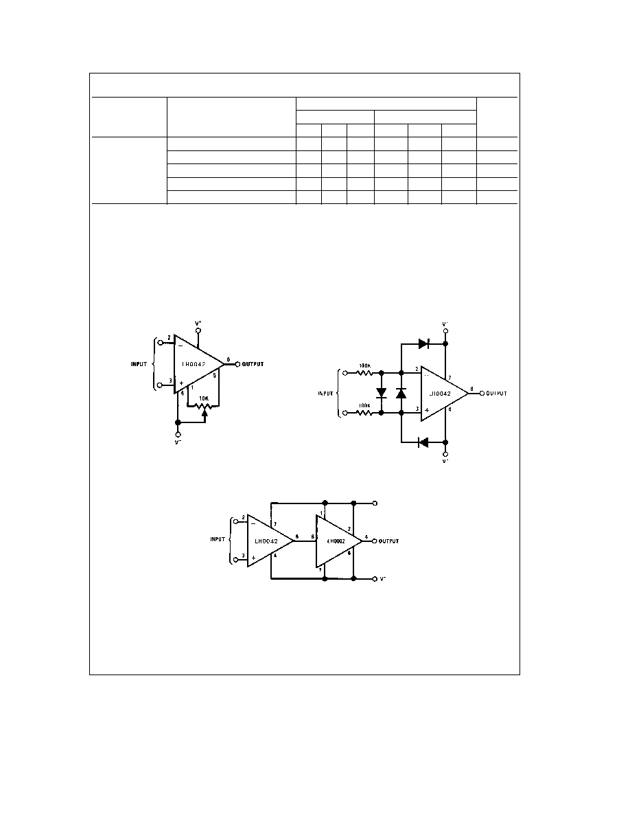
Auxiliary Circuits
(Shown for TO-99 pin out)
Offset Null
TL K 5557 ≠ 5
Protecting Inputs from
g
150V Transients
Note
All diodes are ultra low leakage
TL K 5557 ≠ 6
Boosting Output Drive to
g
100 mA
TL K 5557 ≠ 7
5