 | –≠–ª–µ–∫—Ç—Ä–æ–Ω–Ω—ã–π –∫–æ–º–ø–æ–Ω–µ–Ω—Ç: LH0024 | –°–∫–∞—á–∞—Ç—å:  PDF PDF  ZIP ZIP |
TL K 5552
LH0024
High
Slew
Rate
Operational
Amplifier
February 1995
LH0024 High Slew Rate Operational Amplifier
General Description
The LH0024 LH0024C is a very wide bandwidth high slew
rate operational amplifier intended to fulfill a wide variety of
high speed applications such as buffers to A to D and D to A
converters and high speed comparators The device exhib-
its useful gain in excess of 50 MHz making it possible to use
in video applications requiring higher gain accuracy than is
usually associated with such amplifiers
The LH0024 LH0024C's combination of wide bandwidth
and high slew rate make it an ideal choice for a variety of
high speed applications including active filters oscillators
and comparators as well as many high speed general pur-
pose applications
The LH0024 is guaranteed over the temperature range
b
55 C to
a
125 C whereas the LH0024C is guaranteed
b
25 C to
a
85 C
Features
Y
Very high slew rate
500 V ms at A
V
e
a
1
Y
Wide small signal bandwidth
70 MHz
Y
Wide large signal bandwidth
15 MHz
Y
High output swing
g
12V into 1k
Y
Low input offset
2 mV
Y
Pin compatible with standard IC op amps
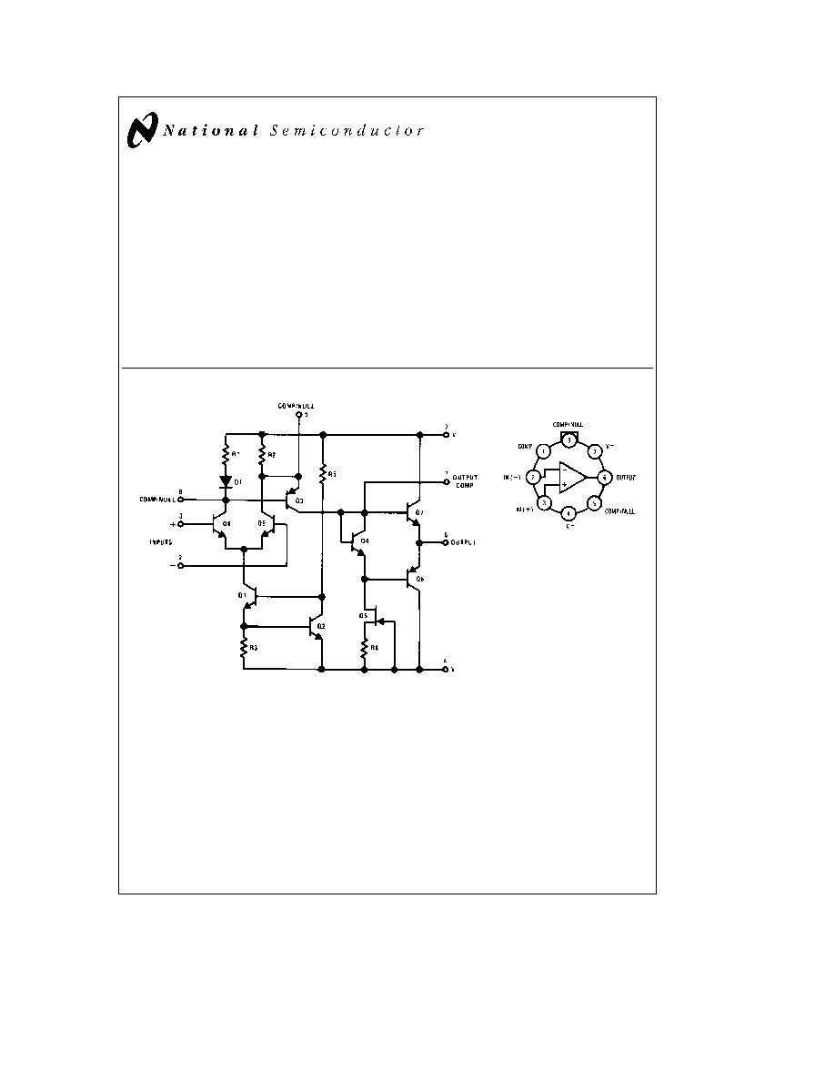
Schematic and Connection Diagrams
TL K 5552 ≠ 1
Metal Can Package
TL K 5552 ≠ 2
Top View
Note
For heat sink use Thermalloy 2230-5
series
Order Number LH0024H
LH0024H-MIL or LH0024CH
See NS Package Number H08B
C1995 National Semiconductor Corporation
RRD-B30M115 Printed in U S A
Absolute Maximum Ratings
If Military Aerospace specified devices are required
please contact the National Semiconductor Sales
Office Distributors for availability and specifications
(Note 2)
Supply Voltage
g
18V
Input Voltage
Equal to Supply
Differential Input Voltage
g
5V
Power Dissipation
600 mW
Storage Temperature Range
b
65 C to
a
150 C
Lead Temperature (Soldering 10 sec )
260 C
ESD rating to be determined
Operating Temperature Range
LH0024
b
55 C to
a
125 C
LH0024C
b
25 C to
a
85 C
DC Electrical Characteristics
(Note 1)
Parameter
Conditions
LH0024
LH0024C
Units
Min
Typ
Max
Min
Typ
Max
Input Offset Voltage
R
S
e
50X T
A
e
25 C
2 0
4 0
5 0
8 0
mV
R
S
e
50X
6 0
10 0
mV
Average Temperature
V
S
e
g
15V R
S
e
50X
Coefficient of Input
b
55 C to 125 C
b
20
b
25
m
V C
Offset Voltage
Input Offset Current
T
A
e
25 C
2 0
5 0
4 0
15 0
m
A
10 0
20 0
m
A
Input Bias Current
T
A
e
25 C
15
30
18
40
m
A
40
50
m
A
Supply Current
12 5
15
12 5
15
mA
Large Signal Voltage
V
S
e
g
15V R
L
e
1k T
A
e
25 C
4
5
3
4
V mV
Gain
V
S
e
g
15V R
L
e
1k
3
2 5
V mV
Input Voltage Range
V
S
e
g
15V
g
12
g
13
g
12
g
13
V
Output Voltage
V
S
e
g
15V R
L
e
1k T
A
e
25 C
g
12
g
13
g
10
g
13
V
Swing
V
S
e
g
15V R
L
e
1k
g
10
g
10
V
Slew Rate
V
S
e
g
15V R
L
e
1k
C
1
e
C
2
e
30 pF
400
500
250
400
V ms
A
V
e a
1 T
A
e
25 C
Common-Mode
V
S
e
g
15V DV
IN
e
g
10V
60
60
dB
Rejection Ratio
R
S
e
50X
Power Supply
g
5V
s
V
S
s g
18V
60
60
dB
Rejection Ratio
R
S
e
50X
Note 1
These specifications apply for V
S
e g
15V and
b
55 C to
a
125 C for the LH0024 and
b
25 C to
a
85 C for the LH0024C
Note 2
Refer to RETS0024 for LH0024H military specifications
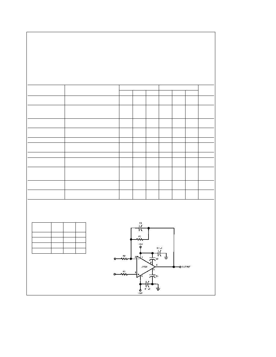
Frequency Compensation
TABLE I
Closed
C
1
C
2
C
3
Loop Gain
100
0
0
0
20
0
0
0
10
0
20 pF
1 pF
1
30 pF
30 pF
3 pF
Frequency Compensation Circuit
TL K 5552 ≠ 6
2
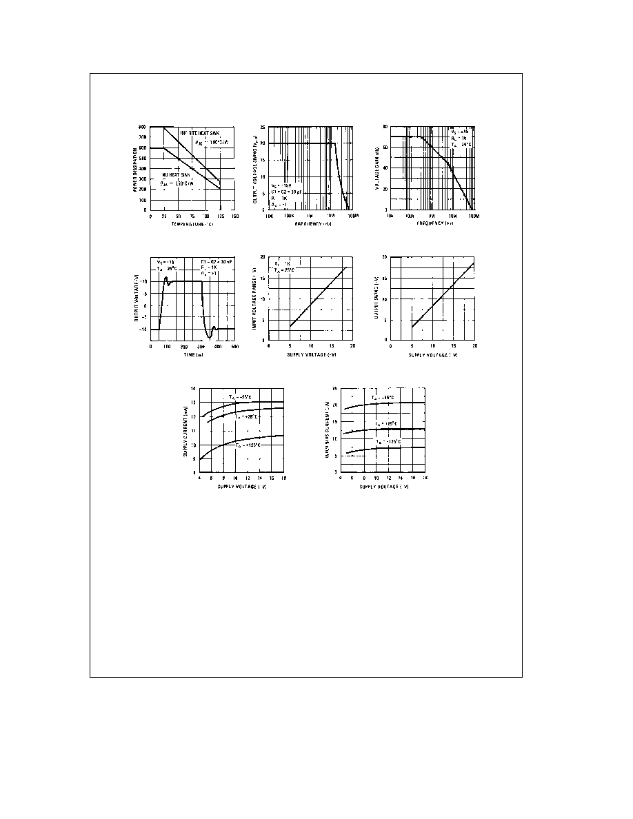
Typical Performance Characteristics
Maximum Power Dissipation
Response
Large Signal Frequency
Response
Open Loop Frequency
Response
Voltage Follower Pulse
Voltage
Input Voltage vs Supply
Output Voltage Swing
Supply Voltage
Supply Current vs
vs Voltage
Input Bias Current
TL K 5552 ≠ 7
Applications Information
LAYOUT CONSIDERATIONS
The LH0024 LH0024C like most high speed circuitry is
sensitive to layout and stray capacitance Power supplies
should be by-passed as near the device as is practicable
with at least 0 01 mF disc type capacitors Compensating
capacitors should also be placed as close to device as pos-
sible
COMPENSATION RECOMMENDATIONS
Compensation schemes recommended in Table 1 work well
under typical conditions However poor layout and long
lead lengths can degrade the performance of the LH0024 or
cause the device to oscillate Slight adjustments in the val-
ues for C1 C2 and C3 may be necessary for a given layout
In particular when operating at a gain of
b
1 C3 may re-
quire adjustment in order to perfectly cancel the input ca-
pacitance of the device
When operating the LH0024 LH0024C at a gain of
a
1
the value of R1 should be at least 1 kX
The case of the LH0024 is electrically isolated from the cir-
cuit hence it may be advantageous to drive the case in
order to minimize stray capacitances
HEAT SINKING
The LH0024 LH0024C is specified for operation without the
use of an explicit heat sink However internal power dissi-
pation does cause a significant temperature rise Improved
offset voltage drift can be obtained by limiting the tempera-
ture rise with a clip-on heat sink such as the Thermalloy
2228B or equivalent
3
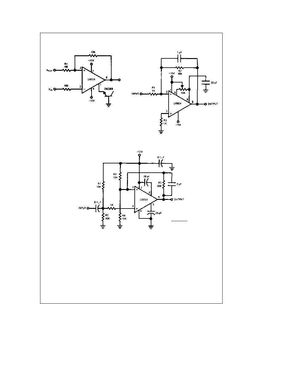
Typical Applications
TTL Compatible Comparator
TL K 5552 ≠ 3
Offset Null
TL K 5552 ≠ 4
Video Amplifier
TL K 5552 ≠ 5
R1
e
R2
e
R3
e
R4
A
V
e
R5
a
(R3 R4)
(R3) (R4)
e
5
4

5