 | –≠–ª–µ–∫—Ç—Ä–æ–Ω–Ω—ã–π –∫–æ–º–ø–æ–Ω–µ–Ω—Ç: LH0091 | –°–∫–∞—á–∞—Ç—å:  PDF PDF  ZIP ZIP |
TL H 5694
LH0091
True
RMS
to
DC
Converter
September 1993
LH0091 True RMS to DC Converter
General Description
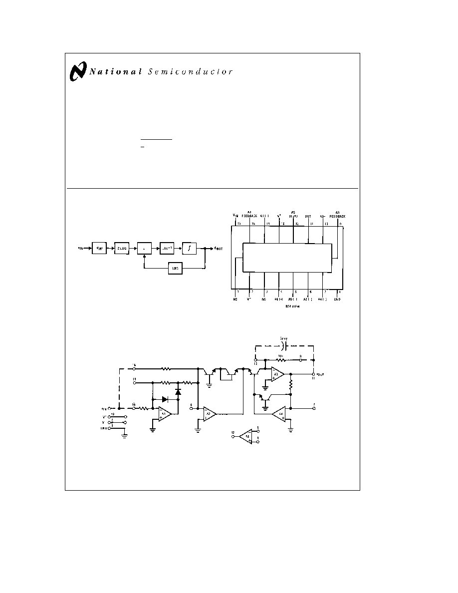
The LH0091 rms to dc converter generates a dc output
equal to the rms value of any input per the transfer function
E
OUT(DC)
e
0
1
T
T
0
E
IN
2
(t) dt
The device provides rms conversion to an accuracy of 0 1%
of reading using the external trim procedure It is possible to
trim for maximum accuracy (0 5 mV
g
0 05% typ) for decade
ranges i e 10 mV
x
100 mV 0 7V
x
7V etc
Features
Y
Low cost
Y
True rms conversion
Y
0 5% of reading accuracy untrimmed
Y
0 05% of reading accuracy with external trim
Y
Minimum component count
Y
Input voltage to
g
15V peak for V
S
e
g
15V
Y
Uncommitted amplifier for filtering gain or high crest
factor configuration
Y
Military or commercial temperature range
Block and Connection Diagrams
Dual-In-Line Package
Order Number LH0091CD
See Package D16D
Dual-In-Line Package
TL H 5694 ≠ 1
Simplified Schematic
TL H 5694 ≠ 2
Note Dotted lines denote external connections
C1995 National Semiconductor Corporation
RRD-B30M115 Printed in U S A
Absolute Maximum Ratings
If Military Aerospace specified devices are required
please contact the National Semiconductor Sales
Office Distributors for availability and specifications
Supply Voltage
g
22V
Input Voltage
g
15V peak
Output Short Circuit Duration
Continuous
Operating Temperature Range
T
MIN
T
MAX
LH0091C
b
25 C
85 C
Storage Temperature Range
LH0091C
b
25 C to
a
85 C
Lead Temp (Soldering 10 seconds)
260 C
Electrical Characteristics
V
S
e
g
15V T
A
e
25 C unless otherwise noted
Transfer Function
e
E
O(DC)
e
0
1
T
T
0
E
IN
2
(t) dt
Parameter
Conditions
Min
Typ
Max
Units
ACCURACY (See Definition of Terms)
Total Unadjusted Error
50 mVrms
s
V
IN
s
7Vrms
(Figure 1)
20
g
0 5
40
g
1 0
mV %
Total Adjusted Error
50 mVrms
s
V
IN
s
7Vrms
(Figure 3)
0 5
g
0 05
1
g
0 2
mV %
Total Unadjusted Error vs Temperature
b
25 C
s
T
A
s
a
70 C
0 25
g
0 2%
mV % C
Total Unadjusted Error vs Supply Voltage
1
mV V
AC PERFORMANCE
Frequency for Specified Adjusted Error
Input
e
7Vrms Sinewave
(Figure 3)
30
70
kHz
Input
e
0 7Vrms Sinewave
(Figure 3)
40
KHz
Input
e
0 1Vrms Sinewave
(Figure 3)
20
kHz
Frequency for 1% Additional Error
Input
e
7Vrms Sinewave
(Figure 3)
100
200
kHz
Input
e
0 7Vrms Sinewave
(Figure 3)
75
kHz
Input
e
0 1Vrms Sinewave
(Figure 3)
50
kHz
Bandwidth (3 dB)
Input
e
7Vrms Sinewave
(Figure 3)
2
MHz
Input
e
0 7Vrms Sinewave
(Figure 3)
1 5
MHz
Input
e
0 1Vrms Sinewave
(Figure 3)
0 8
MHz
Crest Factor
Rated Adjusted Accuracy Using the High
5
10
Crest Factor Circuit
(Figure 5)
INPUT CHARACTERISTICS
Input Voltage Range
For Rated Performance
g
0 05
g
11
Vpeak
Input Impedance
4 5
5
kX
OUTPUT CHARACTERISTICS
Rated Output Voltage
R
L
t
2 5 kX
10
V
Output Short Circuit Current
22
mA
Output Impedance
1
X
POWER SUPPLY REQUIREMENTS
Operating Range
g
5
g
20
V
Quiescent Current
V
S
e
g
15V
14
18
mA
2
Op Amp Electrical Characteristics
V
S
e
g
15V T
A
e
25 C unless otherwise noted
Parameter
Conditions
Min
Typ
Max
Units
V
OS
Input Offset Voltage
R
S
s
10 kX
1 0
10
mV
I
OS
Input Offset Current
4 0
200
nA
I
B
Input Bias Current
30
500
nA
R
IN
Input Resistance
2 5
MX
A
OL
Large Signal Voltage Gain
V
OUT
e
g
10V R
L
t
2 kX
15
160
V mv
V
O
Output Voltage Swing
R
e
10 kX
g
10
g
13
V
V
I
Input Voltage Range
g
10
V
CMRR
Common-Mode Rejection Ratio
R
S
s
10 kX
90
dB
PSRR
Supply Voltage Rejection Ratio
R
S
s
10 kX
96
dB
I
SC
Output Short-Circuit Current
25
mA
S
r
Slew Rate (Unity Gain)
0 5
V ms
BW
Small Signal Bandwidth
1 0
MHz
Typical Performance Characteristics
Error vs Frequency
Error vs Frequency
Error vs Crest Factor
TL H 5694 ≠ 3
Typical Applications
(All applications require power supply by-pass capacitors )
TL H 5694 ≠ 4
C
EXT
t
1mF frequency
t
1 kHz
FIGURE 1 LH0091 Basic Connection (No Trim)
3
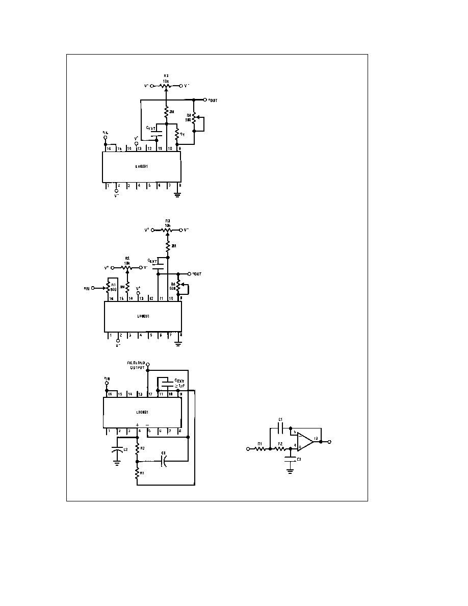
Typical Applications
(Continued)
R
T
e
240k
C
EXT
t
1mF f
t
1 kHz
Note The easy trim procedure is used for ac coupled input signals It in-
volves two trims and can achieve accuracies of 2 mV offset
g
0 1% reading
Procedure
1 Apply 100 mV rms (sine wave) to input adjust R3 until the output reads
100 mV
DC
2 Apply 5 V
rms
(sine wave) to input adjust R4 until the output reads 5 V
DC
3 Repeat steps 1 and 2 until the desired initial accuracy is achieved
FIGURE 2 LH0091 ``Easy Trim'' (For ac Inputs Only)
R1
e
dc symmetry balance
R2
e
Input offset
R3
e
Output offset
R4
e
Gain adjust
Note This procedure will give accuracies of 0 5 mV offset
g
0 05% reading
for inputs from 0 05V peak to 10V peak
Procedure
1 Apply 50 mV
DC
to the input Read and record the output
2 Apply
b
50 mV
DC
to the input Use R2 to adjust for an output of the same
magnitude as in step 1
3 Apply 50 mV to the input Use R3 to adjust the output for 50 mV
4 Apply
b
50 mV to input Use R2 to adjust the output for 50 mV
5 Apply
g
10V alternately to the input Adjust R1 until the output readings
for both polarities are equal (not necessary that they be exactly 10V)
6 Apply 10V to the input Use R4 to adjust for 10V at the output
7 Repeat this procedure to obtain the desired accuracy
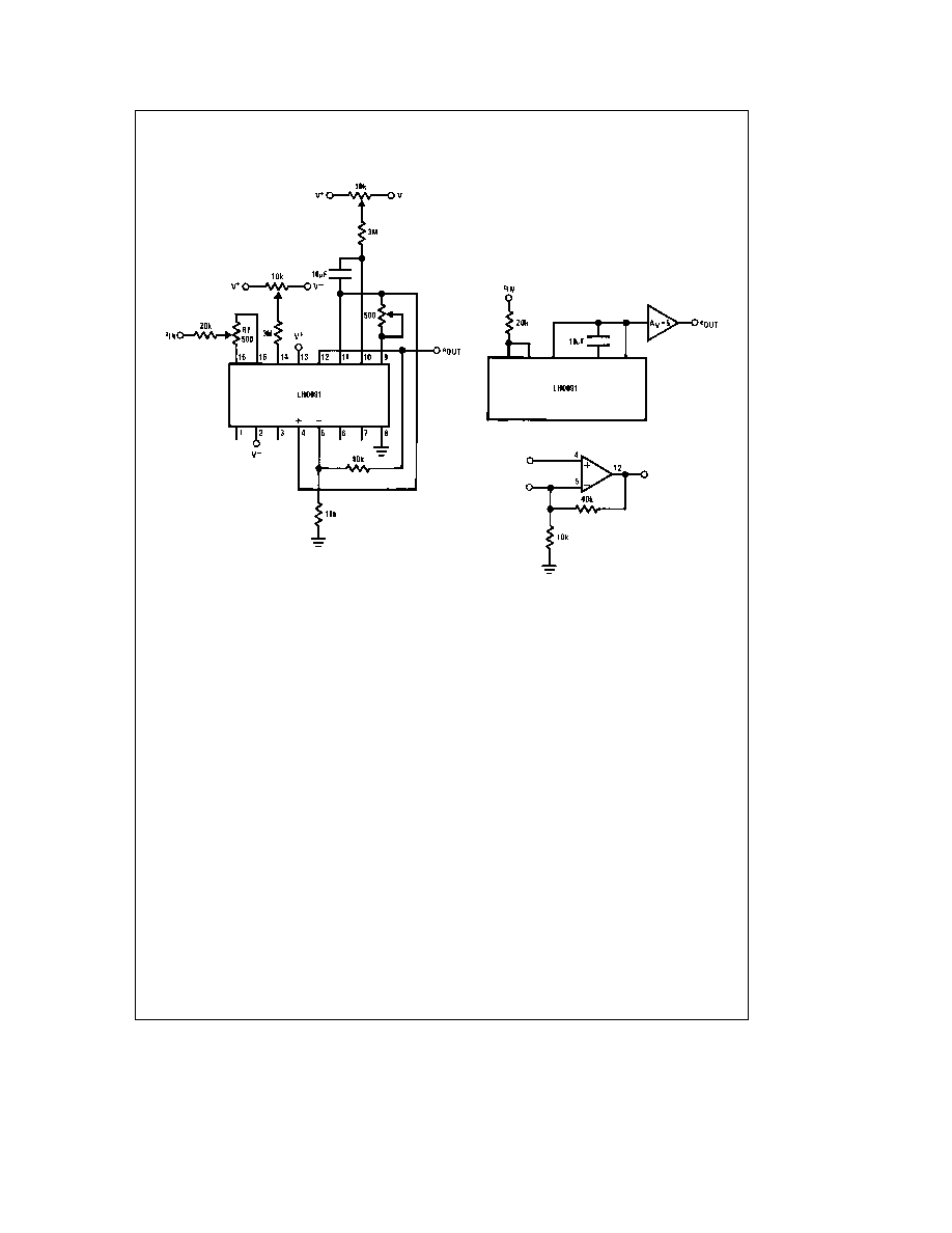
FIGURE 3 LH0091 Standard dc Trim Procedure
Note The additional op amp in the LH0091 may be used as a low pass filter
as shown in
Figure 4
R1
e
R2
e
16k
C1
e
C2
e
1mF
f
O
j
10 Hz
TL H 5694 ≠ 6
FIGURE 4 Output Filter Connection Using the Internal Op Amp
4
Typical Applications
(Continued)
Note When converting signals with a crest factor
t
2 the LH0091 should
be connected as shown Note that this circuit utilizes a 20k resistor to drop
the input current by a factor of five The frequency response will correspond
to a voltage which is 1 5 e
IN
Note that the extra op amp in the LH0091 may be used to build a gain of 5
amplifier to restore the output voltage
TL H 5694 ≠ 7
Note Response time of the dc output voltage is dominated
by the RC time constant consisting of the total resistance
between pins 9 and 10 and the external capacitor C
EX
FIGURE 5 High Crest Factor Circuit
Definition of Terms
True rms to dc Converter
A device which converts any
signal (ac dc ac
a
dc) to the dc equivalent of the rms value
Error
is the amount by which the actual output differs from
the theoretical value Error is defined as a sum of a fixed
term and a percent of reading term The fixed term remains
constant regardless of input while the percent of reading
term varies with the input
Total Unadjusted Error
The total error of the device with-
out any external adjustments
Bandwidth
The frequency at which the output dc voltage
drops to 0 707 of the dc value at low frequency
Frequency for Specified Error
The error at low frequency
is governed by the size of the external averaging capacitor
At high frequencies error is dependent on the frequency
response of the internal circuitry The frequency for speci-
fied error is the maximum input frequency for which the out-
put will be within the specified error band (i e frequency for
1% error means the input frequency must be less than 200
kHz to maintain an output with an error of less than 1% of
the initial reading
Crest Factor
is the peak value of a waveform divided by
the rms value of the same waveform For high crest factor
signals the performance of the LH0091 can be improved by
using the high crest factor connection
5