Original Creation Date: 01/20/00
Last Update Date: 09/17/03
Last Major Revision Date: 07/18/02
MRLM101A-X-RH REV 1B2
MICROCIRCUIT DATA SHEET
SINGLE OPERATIONAL AMPLIFIER - EXTERNALLY COMPENSATED:
ALSO AVAILABLE GUARANTEED TO 100k rd(Si) TESTED TO
MIL-STD-883, METHOD 1019
General Description
The LM101A is a general purpose operational amplifier which features improved performance
over industry standards such as the LM709. Advanced processing techniques make possible
an order of magnitude reduction in input currents, and a redesign of the biasing circuitry
reduces the temperature drift of input current.
This amplifier offers many features which make its application nearly foolproof: overload
protection on the input and output, no latch-up when the common mode range is exceeded,
and freedom from oscillations and compensation with a single 30 pF capacitor. It has
advantages over internally compensated amplifiers in that the frequency compensation can
be tailored to the particular application. For example, in low frequency circuits it can
be overcompensated for increased stability margin. Or the compensation can be optimized
to give more than a factor of ten improvement in high frequency performance for most
applications.
In addition, the device provides better accuracy and lower noise in high impedance
circuitry. The low input currents also make it particularly well suited for long interval
integrators or timers, sample and hold circuits and low frequency waveform generators.
Further, replacing circuits where matched transistor pairs buffer the inputs of
conventional IC op amps, it can give lower offset voltage and a drift at a lower cost.
NS Part Numbers
LM101AH-QMLV
LM101AHRQMLV
LM101AJ-QMLV
LM101AW-QMLV
LM101AWRQMLV
Industry Part Number
LM101A
Prime Die
LM101A
Controlling Document
SEE FEATURES SECTION
Processing
MIL-STD-883, Method 5004
Quality Conformance Inspection
MIL-STD-883, Method 5005
Subgrp Description Temp ( C)
o
1
Static tests at
+25
2
Static tests at
+125
3
Static tests at
-55
4
Dynamic tests at
+25
5
Dynamic tests at
+125
6
Dynamic tests at
-55
7
Functional tests at
+25
8A
Functional tests at
+125
8B
Functional tests at
-55
9
Switching tests at
+25
10
Switching tests at
+125
11
Switching tests at
-55
1

MICROCIRCUIT DATA SHEET
MRLM101A-X-RH REV 1B2
Features
- Offset voltage 3 mV maximum over temperature
- Input current 100 nA maximum over temperature
- Offset current 20 nA maximum over temperature
- Guaranteed drift characteristics
- Offsets guaranteed over entire common mode and supply voltage ranges
- Slew rate of 10V/us as a summing amplifier
CONTROLLING DOCUMENTS:
LM101AH-QMLV 5962-9951501VGA
LM101AHRQMLV 5962R9951501VGA
LM101AJ-QMLV 5962-9951501VPA
LM101AW-QMLV 5962-9951501VHA
LM101AWRQMLV 5962R9951501VHA
2

MICROCIRCUIT DATA SHEET
MRLM101A-X-RH REV 1B2
(Absolute Maximum Ratings)
(Note 1)
Supply Voltage
+22V
Differential Input Voltage
+30V
Input Voltage
(Note 3)
+15V
Ouput Short Circuit Duration
(Note 2)
Continuous
Operating Ambient Temp. Range
-55 C < Ta < +125 C
Maximum Junction Temperature
150 C
Power Dissipation at TA = 25 C
(Note 2)
750mW
H-Pkg (Still Air)
1200mW
H-Pkg (500LF/Min Air Flow)
1000mW
J-Pkg (Still Air)
1500MW
J-Pkg (500LF/Min Air Flow)
Thermal Resistance
ThetaJA
165 C/W
H-Pkg (Still Air)
89 C/W
H-Pkg (500LF/Min Air Flow)
128 C/W
J-Pkg (Still Air)
75 C/W
J-Pkg (500LF/Min Air Flow)
ThetaJC
39 C/W
H-Pkg
26 C/W
J-Pkg
Storage Temperature Range
-65 C <Ta< +150 C
Lead Temperature
300 C
(Soldering, 10 seconds)
ESD Tolerance
(Note 4)
3500V
Note 1:
Absolute Maximum Ratings indicate limits beyond which damage to the device may occur.
Operating Ratings indicate conditions for which the device is intended to be
functional, but do not guarantee specific performance limits. For guaranteed
specifications and test conditions, see the Electrical Characteristics. The
guaranteed specifications apply only for the test conditions listed. Some performance
characteristics may degrade when the device is not operated under the listed test
conditions.
Note 2:
The maximum power dissipation must be derated at elevated temperatures and is
dictated by Tjmax (maximum junction temperature), ThetaJA (package junction to
ambient thermal resistance), and TA (ambient temperature). The maximum allowable
power dissipation at any temperature is Pdmax = (Tjmax - TA)/ThetaJA or the number
given in the Absolute Maximum Ratings, whichever is lower.
Note 3:
For supply voltages less than +15V, the absolute maximum input voltage is equal to
the supply voltage.
Note 4:
Human body model, 100 pF discharged through 1.5k Ohms.
3
MRLM101A-X-RH REV 1B2
MICROCIRCUIT DATA SHEET
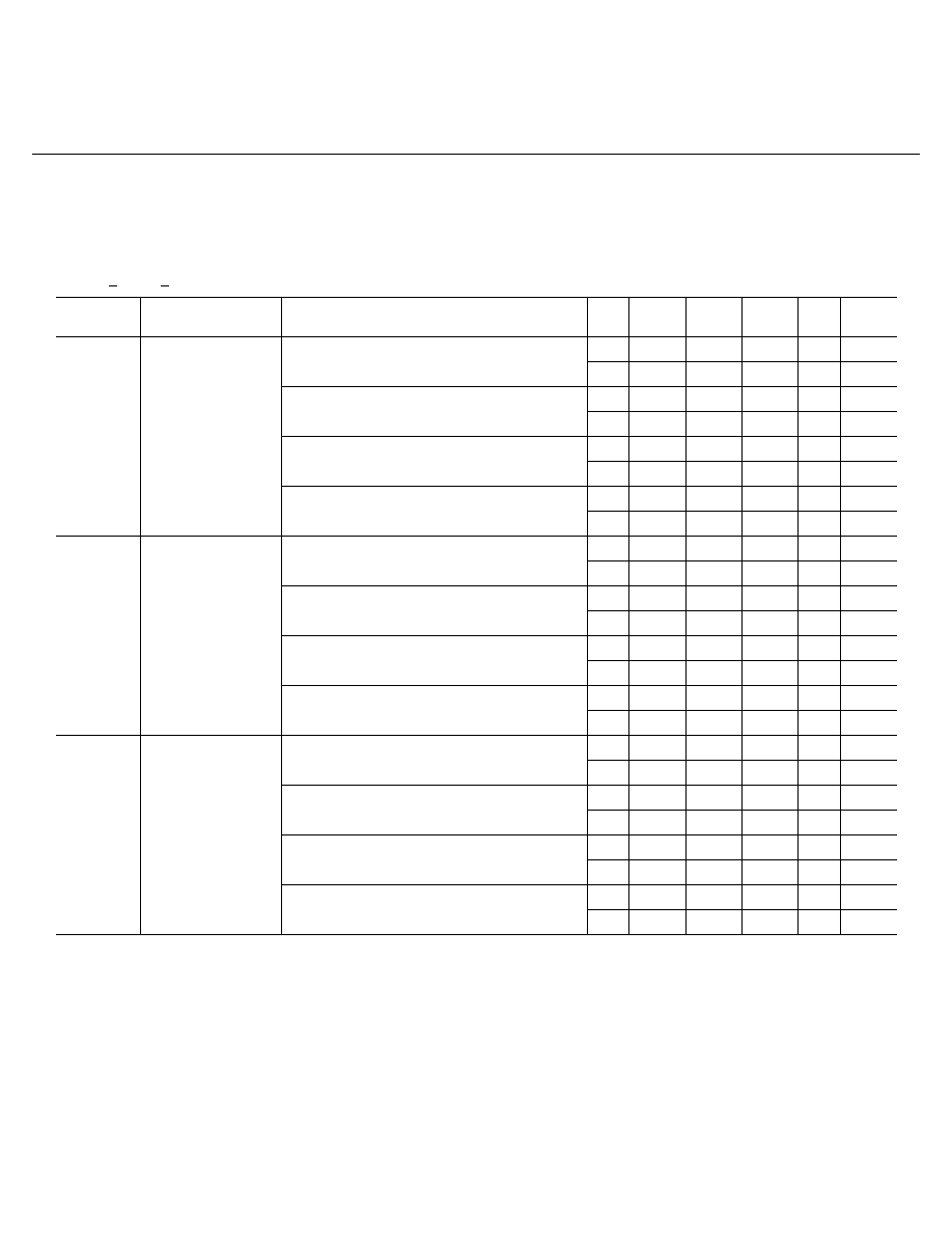
Electrical Characteristics
DC PARAMETERS: See NOTE 3
(The following conditions apply to all the following parameters, unless otherwise specified.)
DC:
+Vcc = +20V, Vcm = 0V, Rs = 50 ohms
SYMBOL
PARAMETER
CONDITIONS
NOTES
PIN-
NAME
MIN
MAX
UNIT
SUB-
GROUPS
Vio
Input Offset
Voltage
+Vcc = 35V, -Vcc = -5V, Vcm = -15V
-2
+2
mV
1
-3
+3
mV
2, 3
+Vcc = 5V, -Vcc = -35V, Vcm = +15V
-2
+2
mV
1
-3
+3
mV
2, 3
Vcm = 0V
-2
+2
mV
1
-3
+3
mV
2, 3
+Vcc = 5V, -Vcc = -5V, Vcm = 0V
-2
+2
mV
1
-3
+3
mV
2, 3
Iio
Input Offset
Current
+Vcc = 35V, -Vcc = -5V, Vcm = -15V,
Rs = 100K Ohms
-10
+10
nA
1, 2
-20
+20
nA
3
+Vcc = 5V, -Vcc = -35V, Vcm = +15V,
Rs = 100K Ohms
-10
+10
nA
1, 2
-20
+20
nA
3
Vcm = 0V, Rs = 100K Ohms
-10
+10
nA
1, 2
-20
+20
nA
3
+Vcc = 5V, -Vcc = -5V, Vcm = 0V,
Rs = 100K Ohms
-10
+10
nA
1, 2
-20
+20
nA
3
Iib+
Input Bias
Current
+Vcc = 35V, -Vcc = -5V, Vcm = -15V,
Rs = 100K Ohms
-0.1
75
nA
1, 2
-0.1
100
nA
3
+Vcc = 5V, -Vcc = -35V, Vcm = +15V,
Rs = 100K Ohms
-0.1
75
nA
1, 2
-0.1
100
nA
3
Vcm = 0V, Rs = 100K Ohms
-0.1
75
nA
1, 2
-0.1
100
nA
3
+Vcc = 5V, -Vcc = -5V, Vcm = 0V,
Rs = 100K Ohms
-0.1
75
nA
1, 2
-0.1
100
nA
3
4
MRLM101A-X-RH REV 1B2
MICROCIRCUIT DATA SHEET
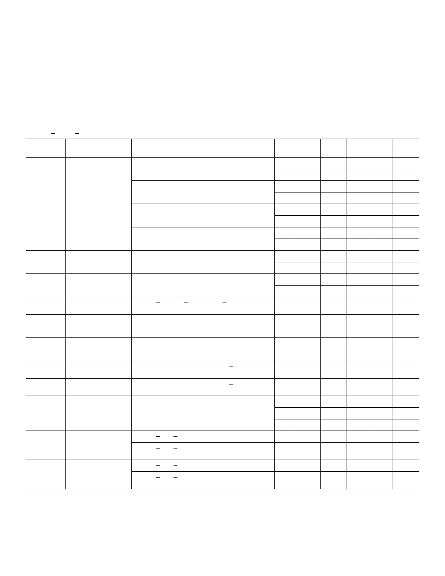
Electrical Characteristics
DC PARAMETERS: See NOTE 3(Continued)
(The following conditions apply to all the following parameters, unless otherwise specified.)
DC:
+Vcc = +20V, Vcm = 0V, Rs = 50 ohms
SYMBOL
PARAMETER
CONDITIONS
NOTES
PIN-
NAME
MIN
MAX
UNIT
SUB-
GROUPS
Iib-
Input Bias
Current
+Vcc = 35V, -Vcc = -5V, Vcm = -15V,
Rs = 100K Ohms
-0.1
75
nA
1, 2
-0.1
100
nA
3
+Vcc = 5V, -Vcc = -35V, Vcm = +15V,
Rs = 100K Ohms
-0.1
75
nA
1, 2
-0.1
100
nA
3
Vcm = 0V, Rs = 100K Ohms
-0.1
75
nA
1, 2
-0.1
100
nA
3
+Vcc = 5V, -Vcc = -5V, Vcm = 0V,
Rs = 100K Ohms
-0.1
75
nA
1, 2
-0.1
100
nA
3
+PSRR
Power Supply
Rejection Ratio
+Vcc = 10V, -Vcc = -20V
-50
+50
uV/V
1
-100
+100
uV/V
2, 3
-PSRR
Power Supply
Rejection Ratio
+Vcc = 20V, -Vcc = -10V
-50
+50
uV/V
1
-100
+100
uV/V
2, 3
CMRR
Common Mode
Rejection Ratio
Vcc = +35V to +5V, Vcm = +15V
80
dB
1, 2,
3
VioADJ(+)
Adjustment for
Input Offset
Voltage
4
mV
1, 2,
3
VioADJ(-)
Adjustment for
Input Offset
Voltage
-4
mV
1, 2,
3
Ios+
Output Short
Circuit Current
+Vcc = 15V, -Vcc = -15V, t < 25mS,
Vcm = -15V
-60
mA
1, 2,
3
Ios-
Output Short
Circuit Current
+Vcc = 15V, -Vcc = -15V, t <25mS,
Vcm = +15V
+60
mA
1, 2,
3
Icc
Power Supply
Current
+Vcc = 15V, -Vcc = -15V
3
mA
1
2.32
mA
2
3.5
mA
3
Delta
Vio/Delta
T
Temperature
Coefficient of
Input Offset
Voltage
+25 C < TA < +125 C
1
-15
+15
uV/ C 2
+25 C < TA < -55 C
1
-18
+18
uV/ C 3
Delta
Iio/Delta
T
Temperature
Coefficient of
Input Offset
Current
+25 C < TA < +125 C
1
-100
+100
pA/ C 2
+25 C < TA < -55 C
1
-200
+200
pA/ C 3
5
MRLM101A-X-RH REV 1B2
MICROCIRCUIT DATA SHEET
Electrical Characteristics
DC PARAMETERS: See NOTE 3(Continued)
(The following conditions apply to all the following parameters, unless otherwise specified.)
DC:
+Vcc = +20V, Vcm = 0V, Rs = 50 ohms
SYMBOL
PARAMETER
CONDITIONS
NOTES
PIN-
NAME
MIN
MAX
UNIT
SUB-
GROUPS
Avs-
Large Signal
(Open Loop)
Voltage Gain
Rl = 2K Ohms, Vout = -15V
2
50
V/mV
4
2
25
V/mV
5, 6
Rl = 10K Ohms, Vout = -15V
2
50
V/mV
4
2
25
V/mV
5, 6
Avs+
Large Signal
(Open Loop)
Voltage Gain
Rl = 2K Ohms, Vout = +15V
2
50
V/mV
4
2
25
V/mV
5, 6
Rl = 10K Ohms, Vout = +15V
2
50
V/mV
4
2
25
V/mV
5, 6
Avs
Large Signal
(Open Loop)
Voltage Gain
Vcc = +5V, Rl = 2K Ohms, Vout = +2V
2
10
V/mV
4, 5,
6
Vcc = +5V, Rl = 10K Ohms, Vout = +2V
2
10
V/mV
4, 5,
6
Vop+
Output Voltage
Swing
Rl = 10K Ohms, Vcm = -20V
+16
V
4, 5,
6
Rl = 2K Ohms, Vcm = -20V
+15
V
4, 5,
6
Vop-
Output Voltage
Swing
Rl = 10K Ohms, Vcm = 20V
-16
V
4, 5,
6
Rl = 2K ohms, Vcm = 20V
-15
V
4, 5,
6
AC PARAMETERS: See NOTE 3
(The following conditions apply to all the following parameters, unless otherwise specified.)
AC:
+Vcc = +20V, Vcm = 0V, Rs = 50 Ohms
Sr+
Slew Rate
Av = 1, Vin = -5V to +5V
0.3
V/uS
7, 8A
0.2
V/uS
8B
Sr-
Slew Rate
Av = 1, Vin = +5V to -5V
0.3
V/uS
7, 8A
0.2
V/uS
8B
TR(tr)
Rise Time
Av = 1, Vin = 50mV
800
nS
7, 8A,
8B
TR(os)
Overshoot
Av = 1, Vin = 50mV
25
%
7
35
%
8A, 8B
NI(BB)
Noise Broadband
BW = 10Hz to 5KHz, Rs = 0 Ohms
15
uVrms 7
NI(PC)
Noise Popcorn
BW = 10Hz to 5KHz, Rs = 100K Ohms
80
uVpk
7
6

MRLM101A-X-RH REV 1B2
MICROCIRCUIT DATA SHEET
Electrical Characteristics
DC PARAMETERS: DRIFT VALUES
(The following conditions apply to all the following parameters, unless otherwise specified.)
DC:
+Vcc = +20V, Vcm = 0V, Rs = 50 Ohms. "Delta calculations performed on JAN S and QMLV devices at group
B, subgroup 5 only".
SYMBOL
PARAMETER
CONDITIONS
NOTES
PIN-
NAME
MIN
MAX
UNIT
SUB-
GROUPS
Vio
Input Offset
Voltage
Vcm = 0V
-0.5
0.5
mV
1
Iib+
Input Bias
Current
Vcm = 0V, Rs = 100K Ohms
-7.5
7.5
nA
1
Iib-
Input Bias
Current
Vcm = 0V, Rs = 100K Ohms
-7.5
7.5
nA
1
Note 1:
Calculated parameter.
Note 2:
Datalog reading of K = V/mV.
Note 3:
Pre and post irradiation limits are identical to those listed under AC and DC
electrical characteristics except as listed in the Post Radiation Limits Table. These
parts may be dose rate sensitive in a space environment and demonstrate enhanced low
dose rate effect. Radiation end point limits for the noted parameters are guaranteed
only for the conditions as specified in MIL-STD-883, Method 1019.5
7

MICROCIRCUIT DATA SHEET
MRLM101A-X-RH REV 1B2
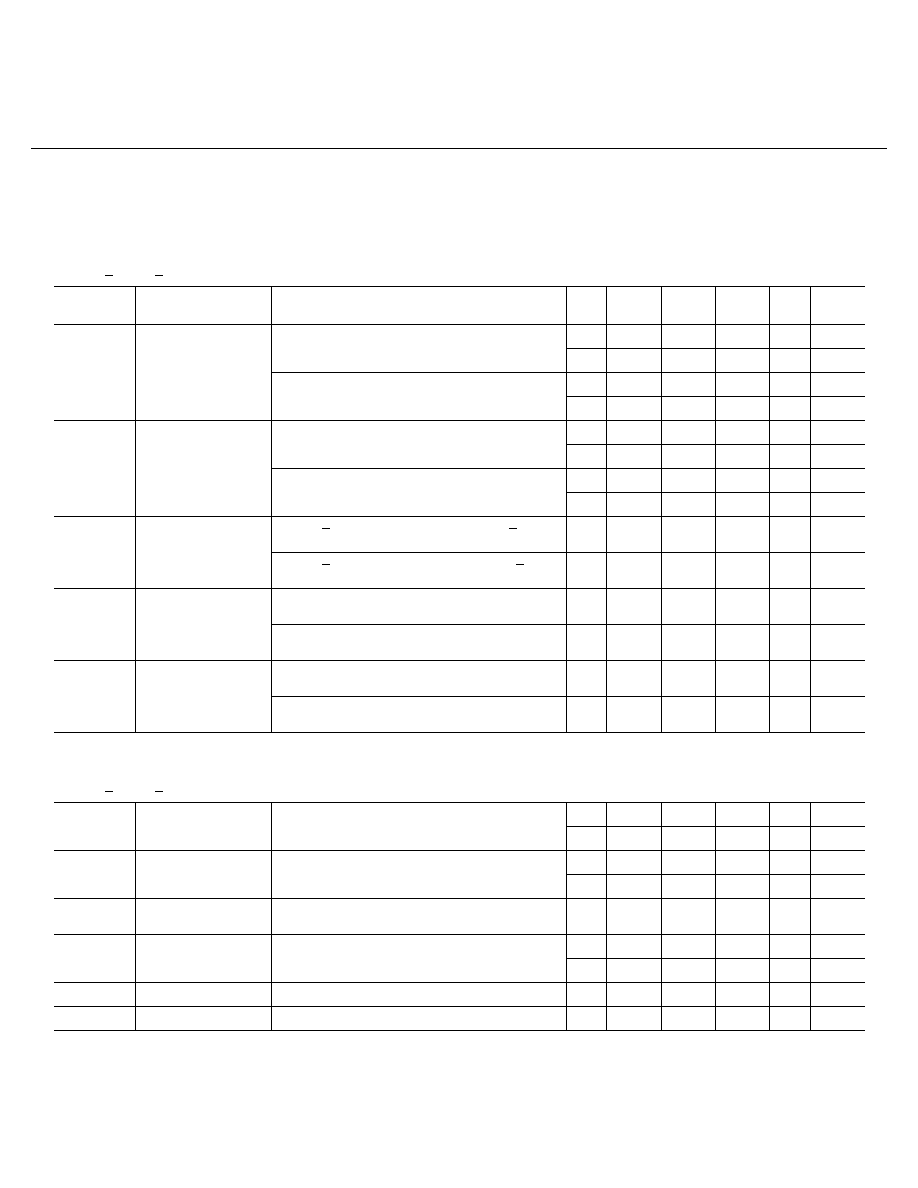
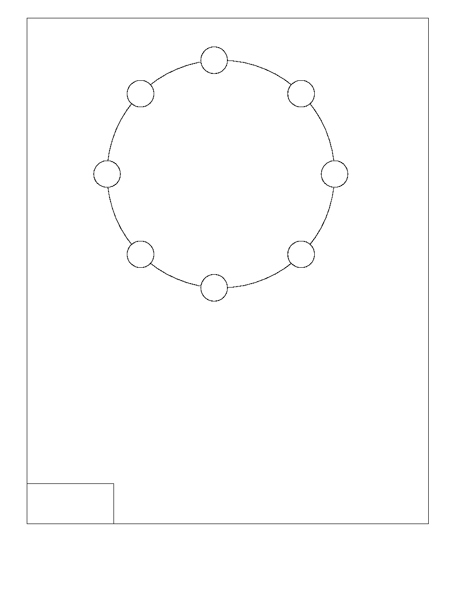
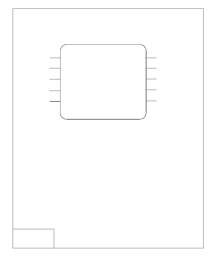
Graphics and Diagrams
GRAPHICS#
DESCRIPTION
05309HRB2
CERDIP (J), 14 LEAD (B/I CKT)
08337HRB2
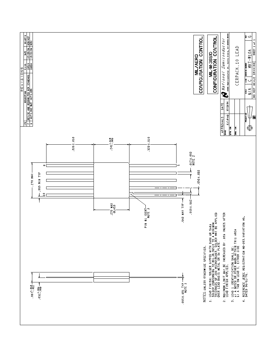
CERPACK (W), 10 LEAD (B/I CKT)
09384HRA4
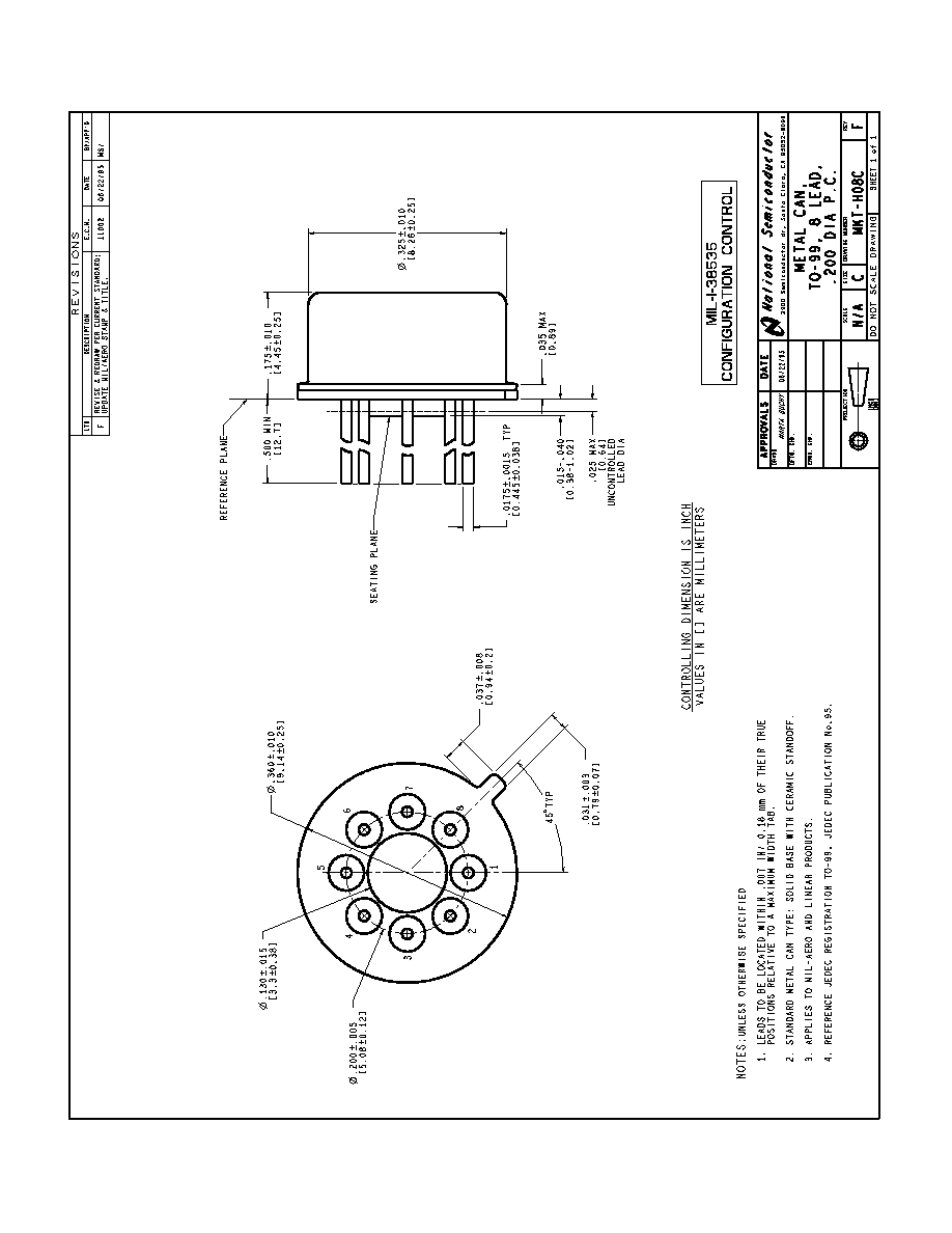
METAL CAN, (H) TO-99,8 LEAD,.200 DIA P.C.(B/I CKT)
09413HRB1
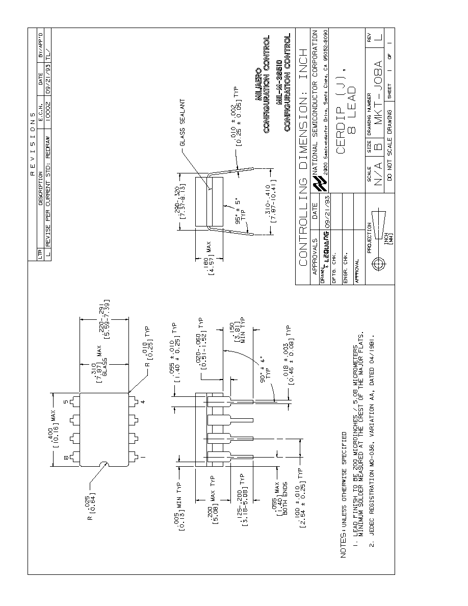
CERDIP (J), 8 LEAD (B/I CKT)
H08CRF
METAL CAN (H), TO-99, 8LD .200 DIA P.C. (P/P DWG)
J08ARL
CERDIP (J), 8 LEAD (P/P DWG)
P000178A
METAL CAN (H), 8 LEAD (PINOUT)
P000180A
CERPACK (W), 10 LEAD (PINOUT)
P000226A
CERDIP (J), 8 LEAD (PINOUT)
W10ARG
CERPACK (W), 10 LEAD (P/P DWG)
See attached graphics following this page.
8
N
�
��
� �
�
�
�
�
N
�
��
� �
�
�
�
�
�
�
�
�
N
�
��
� �
�
�
�
�
�
MICROCIRCUIT DATA SHEET
MRLM101A-X-RH REV 1B2
Revision History
Rev
ECN #
Rel Date
Originator
Changes
0A0
M0003656
05/08/00
Rose Malone
Initial MDS Release: MRLM101A-X-RH, Rev. 0A0
0B0
M0003678
04/08/02
Rose Malone
Update MDS: MRLM101A-X-RH, Rev. 0A0 to MRLM101A-X-RH,
Rev. 0B0. Typo error in Features Section Controlling
Documents: SMD Suffix VPA should be QPA for
LM101AJRQML.
0C0
M0003990
08/13/02
Rose Malone
Update MDS: MRLM101A-X-RH, Rev. 0B0 to MRLM101A-X-RH,
Rev. 0C0. Deleted reference for the following NSID's
from Main Table, Features Section and Graphics
Section. LM101AHRQML , LM101AJRQML,
LM101AJRQMLV, LM101AWRQML, LM101AWRQMLV product
un-available.
1A1
M0004032
09/17/03
Rose Malone
Update MRLM101A-X-RH, Rev. 0C0 to MRLM101A-X-RH, Rev.
1A1. Added to Main Table and Features Section NSID's
LM101AH-QMLV and LM101AJ-QMLV, to Absolute Section J
pkg Thermal Resistance information and Graphics
Section J pkg Mkt Dwg, B/I Ckt, Pin Out. Created QMLV
NSID's to Replace the JL101 Space Level Products.
Changed Electrical Section AC Parameter TR(os)
Subgroups 8A, 8B from 25% to 35%. Subgroups 8A, 8B
unable to meet 25% Overshoot.
1B2
M0004301
09/17/03
Rose Malone
Update MD: MRLM101A-X-RH, Rev. 1A1 to MRLM101A-X-RH,
Rev. 1B2. Added W package reference to Main Table,
Features Section and Graphics Section. Changed ESD
Rating from 2000V to 3500V.
9